Table of Contents
Advertisement
Quick Links
Notes: Please refer to the Original Service Manual for :
CD Mechanism Unit (DLS6C), Order No. MD0803034CE
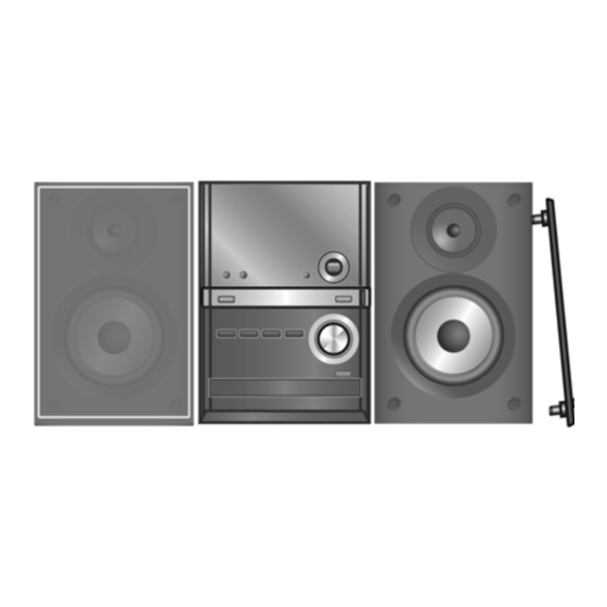
Speaker system SB-PM48EG-K, Order No. PSG0902008CE
TABLE OF CONTENTS
1 Safety Precautions----------------------------------------------- 3
1.1. General Guidelines---------------------------------------- 3
1.2. Before Repair and Adjustment ------------------------- 4
1.3. Protection Circuitry ---------------------------------------- 4
1.4. Safety Part Information----------------------------------- 4
2 Warning -------------------------------------------------------------- 5
to Electrostatically Sensitive (ES) Devices---------- 5
2.2. Precaution of Laser Diode------------------------------- 6
2.4. Handling Precaution for Traverse Unit --------------- 8
Model No.
Product Color: (K)...Black Type
PAGE
3 Service Navigation --------------------------------------------- 10
3.1. Service Information -------------------------------------- 10
4 Specifications ---------------------------------------------------- 11
5 Location of Controls and Components------------------ 12
5.1. Main Unit Key Button Operations -------------------- 12
5.2. Remote Control Key Button Operations------------ 13
5.3. Media Information---------------------------------------- 14
6 Self-diagnostic and special mode setting -------------- 15
6.1. Entering into Self-diagnostic Mode ------------------ 15
6.2. Self-diagnostic Function Error Code ---------------- 15
6.3. Entering into Doctor Mode ----------------------------- 16
© Panasonic Corporation 2010. All rights reserved.
Unauthorized copying and distribution is a violation of
law.
CD Stereo System
SA-PM42EG
SA-PM42EF
SA-PM42EP
PSG1002016CE
PAGE
Advertisement
Table of Contents

Related Manuals for Panasonic SA-PM42EP


Summary of Contents for Panasonic SA-PM42EP
-
Page 1: Table Of Contents
2.3. Service caution based on Legal restrictions -------- 7 6.2. Self-diagnostic Function Error Code ---------------- 15 2.4. Handling Precaution for Traverse Unit --------------- 8 6.3. Entering into Doctor Mode ----------------------------- 16 © Panasonic Corporation 2010. All rights reserved. Unauthorized copying and distribution is a violation of law. - Page 2 7 Troubleshooting Guide---------------------------------------- 20 19 Printed Circuit Board------------------------------------------ 87 8 Service Fixture & Tools --------------------------------------- 21 19.1. CD SERVO P.C.B. and TRANSFORMER 9 Disassembly and Assembly Instructions --------------- 22 P.C.B. ------------------------------------------------------- 87 9.1. Disassembly flow chart --------------------------------- 23 19.2. MAIN P.C.B.----------------------------------------------- 88 9.2.
-
Page 3: Safety Precautions
1 Safety Precautions 1.1. General Guidelines 1. When servicing, observe the original lead dress. If a short circuit is found, replace all parts which have been overheated or damaged by the short circuit. 2. After servicing, see to it that all the protective devices such as insulation barriers, insulation papers shields are properly installed. -
Page 4: Before Repair And Adjustment
1.2. Before Repair and Adjustment Caution : DO NOT SHORT-CIRCUIT DIRECTLY (with a screwdriver blade, for instance), as this may destroy solid state devices. After repairs are completed, restore power gradually using a variac, to avoid overcurrent. • Current consumption at AC 220-240V, at 50Hz in NO SIGNAL mode (at volume min in FM Tuner mode) should be ~150 mA. 1.3. -
Page 5: Warning
2 Warning 2.1. Prevention of Electro Static Discharge (ESD) to Electrostatically Sensi- tive (ES) Devices Some semiconductor (solid state) devices can be damaged easily by static electricity. Such components commonly are called Elec- trostatically Sensitive (ES) Devices. Examples of typical ES devices are integrated circuits and some field-effect transistors and semiconductor “chip”... -
Page 6: Precaution Of Laser Diode
2.2. Precaution of Laser Diode CAUTION! THIS PRODUCT UTILIZES A LASER. USE OF CONTROLS OR ADJUSTMENTS OR PERFORMANCE OF PROCEDURES OTHER THAN THOSE SPECIFIED HEREIN MAY RESULT IN HAZARDOUS RADIATION EXPOSURE. Caution: This product utilizes a laser diode with the unit turned "on", invisible laser radiation is emitted from the pickup lens. Wavelength: 785 nm (CD) Maximum output radiation power from pickup: 100 μW/VDE Laser radiation from the pickup unit is safety level, but be sure the followings:... -
Page 7: Service Caution Based On Legal Restrictions
2.3. Service caution based on Legal restrictions 2.3.1. General description about Lead Free Solder (PbF) The lead free solder has been used in the mounting process of all electrical components on the printed circuit boards used for this equipment in considering the globally environmental conservation. The normal solder is the alloy of tin (Sn) and lead (Pb). -
Page 8: Handling Precaution For Traverse Unit
2.4. Handling Precaution for Traverse Unit The laser diode in the optical pickup unit may break down due to static electricity of clothes or human body. Special care must be taken avoid caution to electrostatic breakdown when servicing and handling the laser diode in the traverse unit. Cautions to Be Taken in Handling the Optical Pickup Unit 2.4.1. - Page 9 2.4.2.2. Human body grounding 1. Use the anti-static wrist strap to discharge the static electricity form your body (Figure 2). Figure 2...
-
Page 10: Service Navigation
3 Service Navigation 3.1. Service Information This service manual contains technical information which will allow service perssonnel’s to understand and service this model. Please place orders using the parts list and not the drawing reference numbers. If the circuit is changed or modified, this information will be followed by supplement service manual to be filed with original service manual. -
Page 11: Specifications
1. Specifications are subject to change without notices. Mass and dimensions are approximate. 2. Total harmonic distortion is measured by the digital spectrum ana- lyzer. System : SC-PM42EF-K Music center: SA-PM42EF-K Speaker: SB-PM48EG-K System : SC-PM42EG-K Music center: SA-PM42EG-K Speaker: SB-PM48EG-K System : SC-PM42EP-K Music center: SA-PM42EP-K Speaker: SB-PM48EG-K... -
Page 12: Location Of Controls And Components
5 Location of Controls and Components 5.1. Main Unit Key Button Operations... -
Page 13: Remote Control Key Button Operations
5.2. Remote Control Key Button Operations... -
Page 14: Media Information
5.3. Media Information Note Charging the iPod This unit can play MP3 files and CD-DA format audio CD-R/RW that have been finalized. iPod will start recharging regardless of whether this unit is in On or Standby condition. This unit can access up to 99 tracks. “IPOD ”... -
Page 15: Self-Diagnostic And Special Mode Setting
6 Self-diagnostic and special mode setting This unit is equipped with features of self-diagnostic & special mode setting for checking the functions & reliability. 6.1. Entering into Self-diagnostic Mode Here is the procedure to enter into self-diagnostic mode: Step 1 : Switch to CD function Step 2 : Press the [ ] key of the main set for more than 2 seconds. -
Page 16: Entering Into Doctor Mode
6.3. Entering into Doctor Mode Here is the procedure to enter into doctor mode : Press [ ] button on main unit follow by [4] and [7] on remote control. The FL shall display :- To exit the Doctor mode Press button on main unit or remote control. -
Page 17: Doctor Mode Table
6.3.2. Doctor Mode Table 2 Item FL Display Key Operation Mode Name Description Front Key FL Display Test To check the FL segments In Doctor Mode: display (All segments will 1. Press [DIMMER] button on light up) remote control. To cancel, press [0] button on remote control. - Page 18 Item FL Display Key Operation Mode Name Description Front Key USB Test Mode To check for USB operation. In Doctor Mode: 1. Select to USB mode. 2. Press [2] button on remote con- trol. To exit Doctor Mode, press button The display will appear after 3s, on main unit or remote control.
- Page 19 6.3.5. DLS6 Combination Test First Track Access First Track Play 10 s Last Track Access Count Up Last Track Play 10 s OPEN Operation OPEN wait for 1 s CLOSE Operation...
-
Page 20: Troubleshooting Guide
7 Troubleshooting Guide... -
Page 21: Service Fixture & Tools
8 Service Fixture & Tools Prepare service tools before proccess service position. Service Tools Remarks Main P.C.B. (CN901) - Panel P.C.B. (CN900) REEX1022 (11P FFC) -
Page 22: Disassembly And Assembly Instructions
9 Disassembly and Assembly Instructions Caution Note: • This section describes the disassembly and/or assembly procedures for all major printed circuit boards & main compo- nents for the unit. (You may refer to the section of “Main components and P.C.B Locations” as described in the service manual) •... -
Page 23: Disassembly Flow Chart
9.1. Disassembly flow chart The following chart is the procedure for disassembling the casing and inside parts for internal inspection when carrying out the ser- vicing. To assemble the unit, reverse the steps shown in the chart below. -
Page 24: Main Parts Location Diagram
9.2. Main Parts Location Diagram... -
Page 25: Disassembly Of Top Cabinet Assembly
9.3. Disassembly of Top Cabinet Step 3 : Remove 3 screws. Assembly Step 1 : Remove 3 screws. Step 4 : Lift up the Top Cabinet Assembly and remove it. Caution : During assembling, ensure the Top Cabinet Assembly is seated properly. Step 2 : Remove 3 screws. -
Page 26: Disassembly Of Headphone P.c.b
Step 5 : Upset the Top Cabinet Assembly as arrow shown. 9.4. Disassembly Headphone Step 6 : Place a support block underneath the Top Cabinet P.C.B. Assembly. • Refer to “Disassembly of Top Cabinet Assembly”. Step 1 : Remove 2 screws. Step 2 : Release guide and remove Headphone P.C.B.. -
Page 27: Disassembly Of Ipod P.c.b
9.5. Disassembly of iPod P.C.B. 9.6. Disassembly of iPod Lid • Refer to “Disassembly of Top Cabinet Assembly”. • Refer to “Disassembly of iPod P.C.B.” Step 1 : Remove 2 screws. Step 1 : Remove 1 screw. Step 2 : Remove iPod P.C.B.. Caution : During assembling, ensure the iPod P.C.B. - Page 28 Step 2 : Using minus screwdriver slightly to release the iPod Step 3 : Slightly lift up the iPod cover lid as arrow shown. cover lid from the catch. Caution : Do not exert strong force to the iPod cover lid during removal.
- Page 29 Caution 1 : During assembling, ensure the iPod cover lid is Step 6 : Release the spring from the shaft of the top cabinet. properly seated on the locators and slot into the hole of the top cabinet. Caution 2 : During assembling, ensure the iPod cover lid is properly catch to the top cabinet and a “click”...
- Page 30 Step 7 : Release the spring from the shaft of the iPod lid. Step 8 : Remove the spring as arrow shown. Caution : Keep the spring in a safe place and place it back during assembling. Step 9 : Using minus screwdriver to release the shaft (A) of the iPod lid.
- Page 31 Step 10 : Lift up one side of the iPod lid. Step 12 : Lift up the iPod lid as arrow shown. Step 11 : Using minus screwdriver to release the shaft (B). Step 13 : Remove the iPod lid as arrow shown. Caution : Do not exert strong force to the iPod lid during removal.
-
Page 32: Disassembly Of Front Panel Assembly
9.7. Disassembly of Front Panel Step 4 : Release both locators. Step 5 : Release 3 catches from the bottom. Assembly Step 6 : Detach the Front Panel Assembly. • Refer to “Disassembly of Top Cabinet Assembly”. Caution : Do not attempt to exert strong force when detaching the front panel assembly. -
Page 33: Disassembly Of Usb P.c.b
9.8. Disassembly of USB P.C.B. Caution : During assembling, ensure that the USB P.C.B. is firmly catched and properly seated on the guides and loca- • Refer to “Disassembly of Top Cabinet Assembly”. tors. • Refer to “Disassembly of Front Panel Assembly”. Step 1 : Remove 2 screws. -
Page 34: Disassembly Of Panel P.c.b
9.9. Disassembly of Panel P.C.B. Step 3 : Release catch • Refer to “Disassembly of Top Cabinet Assembly”. • Refer to “Disassembly of Front Panel Assembly”. • Refer to (Step 1) of Item 9.8. Step 1 : Remove Volume Knob. Step 4 : Slightly lift up the Panel P.C.B.. -
Page 35: Disassembly Of Fl Window
Step 5 : Slot out and remove the Panel P.C.B. as arrow shown. 9.10. Disassembly of FL Window • Refer to “Disassembly of Top Cabinet Assembly”. • Refer to “Disassembly of Front Panel Assembly”. • Refer to (Step 1) of Item 9.8. •... -
Page 36: Disassembly Of Centre Ornament
9.11. Disassembly of Centre Orna- 9.12. Disassembly of CD Lid ment • Refer to “Disassembly of Front Panel Assembly” • Refer to “Disassembly of Top Cabinet Assembly”. Step 1 : Lift the spring out of the hook. • Refer to “Disassembly of Front Panel Assembly”. Caution : Keep the spring in a safe place and place it back •... - Page 37 Step 2 : Move the shaft (L) of the CD Lid in the direction ofar- Step 4 : Remove the CD Lid in the direction of arrow shown. row shown. Step 3 : Move the shaft (R) of the CD Lid in the direction of arrow shown.
-
Page 38: Disassembly Of Cd Mechanism Unit (Dls6C)
9.13. Disassembly of CD Mecha- 9.14. Disassembly of Power P.C.B. nism Unit (DLS6C) • Refer to “Disassembly of Top Cabinet Assembly”. • Refer to “Disassembly of Front Panel Assembly”. • Refer to “Disassembly of Top Cabinet Assembly”. • Refer to “Disassembly of Front Panel Assembly”. Step 1 : Remove 1 screw. - Page 39 Step 4 : Remove 2 screws. Caution 2 : Ensure the 4P wire is properly dressed into the hook of Power P.C.B. and prevent touching the heatsink Step 5 : Remove Power P.C.B. as arrow shown. unit. Caution 1 : Ensure the heatsink supports are seat properly.
-
Page 40: Replacement Of Power Amp Ic (Ic5101)
9.15. Replacement of Power Amp IC Step 3 : Remove Power Amp IC (IC5101). (IC5101) • Refer to “Disassembly of Power P.C.B.” Caution : Handle the heatsink unit P.C.B. with caution due to its high temperature after prolonged use. Touching it may lead to injuries. - Page 41 • Assembly of Power Amp IC (IC5101) Step 4 : Solder pins of the Power Amp IC (IC5101) on the sol- der side of Power P.C.B.. Step 1 : Apply grease to the heatsink unit. Caution : Check for solderability of the Power Amp IC. Step 2 : Install Power Amp IC onto Power P.C.B..
-
Page 42: Disassembly Of Main P.c.b
9.16. Disassembly of Main P.C.B. Step 4 : Detach 7P cable at connector (CN5903) on Trans- former P.C.B.. • Refer to “Disassembly of Top Cabinet Assembly”. • Refer to “Disassembly of Front Panel Assembly”. • Refer to “Disassembly of Power P.C.B.”. Step 1 : Detach 2P cable at connector (CN100) on Main P.C.B.. - Page 43 Step 6 : Use a paper clip to release the catch. Caution : Ensure the Main P.C.B. fix onto the catches. Step 7 : Remove Main P.C.B..
-
Page 44: Disassembly Of Fan Unit
9.17. Disassembly of Fan Unit Step 3 : Release 2 catches. Step 4 : Remove 2P cable from the holder. • Refer to “Disassembly of Top Cabinet Assembly”. Step 5 : Remove Fan Unit. • Refer to “Disassembly of Front Panel Assembly”. Caution : Ensure the Fan Unit is seated properly onto the •... -
Page 45: Disassembly Of Transformer P.c.b
9.18. Disassembly of Transformer Step 4 : Place a support block to tilt the unit as shown. Step 5 : Remove 4 screws. P.C.B. • Refer to “Disassembly of Top Cabinet Assembly”. • Refer to “Disassembly of Front Panel Assembly”. Step 1 : Detach 4P cable at connector (CN5101) on Power P.C.B.. -
Page 46: Replacement Of Transistor (Q5901)
Step 7 : Remove Transformer cover P.C.B. and Trans spacers. 9.19. Replacement Transistor Caution : Keep them in safe place for assembling use. (Q5901) • Refer to “Disassembly of Transformer P.C.B.” Caution : Handle the heatsink unit and P.C.B. with caution due to its high temperature after prolonged use. - Page 47 Step 3 : Remove Transistor (Q5901). • Assembly of Transistor (Q5901) Step 1 : Apply grease to the heatsink unit. Step 2 : Install Transistor (Q5901) onto Transformer P.C.B.. Caution : Ensure the pins are inserted & seated properly on Transformer P.C.B.. Step 3 : Fix the Transistor (Q5901) onto the heatsink unit with 1 screw.
-
Page 48: Disassembly Of Cd Servo P.c.b
Step 4 : Solder pin of the Transistor (Q5901) on the solder side 9.20. Disassembly of CD Servo of Main P.C.B.. P.C.B. Caution : Check for solderability of the Transistor (Q5901). • Refer to “Disassembly of CD Mechanism Unit (DLS6C).” Step 1 : Remove 3 screws. - Page 49 Step 5 : Detach 16P FPC at the connector (CN7001) on CD Servo P.C.B.
-
Page 50: Disassembly And Assembly Of Traverse Unit
10 Disassembly and Assembly of Traverse Unit 10.1. Disassembling Procedures Step 3 : Slide out the traverse unit as arrow shown. Step 1 : Release the guide. Step 2 : Push the traverse slide plate (rib), ensure both grooves are opened. Caution : Ensure the OPU is face upwards, avoid touching the surface of the traverse unit. -
Page 51: Assembling Procedure
10.2. Assembling Procedure Step 1 : Release the guide. Step 2 : Push the traverse slide plate (rib), ensure both grooves are opened. Caution : Removal of the short pin is necessary for replacement of new traverse unit. - Page 52 Step 3 : Slot the traverse unit at approximately 45° into the mecha chassis as arrow shown. Caution : Ensure the bosses fix exactly onto the guides. Step 4 : Release the guide. Step 5 : Push the traverse slide plate (rib) to lock the traverse unit in.
-
Page 53: Service Position
11 Service Position Note: For description of the disassembly procedures, see the Section 9 11.1. Checking & Repairing USB Step 3 : Release both locators. Step 4 : Release 3 catches. P.C.B. Step 5 : Slighly detach Front Panel Assembly. Step 1 : Remove Top Cabinet Assembly. - Page 54 Step 7 : Place a support block underneath the Top Cabinet Step 11 : Place a support block underneath the USB P.C.B.. Assembly. Step 12 : Check & repair USB P.C.B. according to the diagram Step 8 : Connect 14P FFC at connector (CN350) on Main shown.
-
Page 55: Checking & Repairing Panel P.c.b
11.2. Checking & Repairing Panel Step 8 : Lay an insulating material on Panel P.C.B.. Step 9 : Attach extension cable REEX1022 (11P FFC from P.C.B. CN901 on Main P.C.B. to CN900 on Panel P.C.B.). Step 10 : Connect 4P cable at connector (CN5902) on Trans- Step 1 : Remove Top Cabinet Assembly. -
Page 56: Checking & Repairing Cd Servo P.c.b
11.3. Checking & Repairing Step 9 : Connect 22P FFC at connector (CN370) on Main P.C.B.. Servo P.C.B. Note : Insert CD before Checking CD Servo P.C.B. Step 1 : Remove Top Cabinet Assembly. Step 2 : Remove Front Panel Assembly. Step 3 : Remove CD Mechanism Unit (DLS6C). -
Page 57: Checking & Repairing Power P.c.b
11.4. Checking & Repairing Power Step 7 : Put insulating material under Power P.C.B.. P.C.B. Step 1 : Remove Top Cabinet Assembly. Step 2 : Remove Front Panel Assembly. Step 3 : Remove 1 screw. Step 8 : Place a support block underneath the Top Cabinet Assembly. -
Page 58: Checking & Repairing Transformer P.c.b
Step 11 : Connect 11P FFC at connector (CN901) on Main 11.5. Checking & Repairing Trans- P.C.B.. former P.C.B. Step 12 : Connect 22P FFC at connector (CN380) on USB P.C.B.. Step 13 : Connect 4P cable at connector (CN5902) on Trans- Step 1 : Remove Top Cabinet Assembly. - Page 59 Step 14 : Connect 4P cable at connector (CN5101) on Power Step 19 : Connect 2P cable (Fan Unit) at connector (CN100) P.C.B.. on Main P.C.B.. Step 15 : Connect 7P cable at connector (CN5903) on Trans- Step 20 : Check & repair Transformer P.C.B. according to the former P.C.B..
-
Page 60: Checking & Repairing Main P.c.b
11.6. Checking & Repairing Main P.C.B. • Refer to (Step 1 - Step 19) of item 11.5 Step 1 : Flip over Fan Unit. Step 2 : Check & repair Main P.C.B. according to the diagram shown. -
Page 61: Voltage Measurement & Waveform Chart
12 Voltage Measurement & Waveform Chart Note: • Indicated voltage values are the standard values for the unit measured by the DC electronic circuit tester (high-impedance) with the chassis taken as standard. Therefore, there may exist some errors in the voltage values, depending on the internal impedance of the DC circuit tester. •... -
Page 62: Usb P.c.b
12.2. USB P.C.B. REF NO. IC900 MODE CD PLAY STANDBY IC900 REF NO. MODE CD PLAY STANDBY IC900 REF NO. MODE CD PLAY STANDBY IC900 REF NO. MODE CD PLAY STANDBY SA-PM42EF/EG/EP USB P.C.B. -
Page 63: Main P.c.b. (1/2)
12.3. MAIN P.C.B. (1/2) REF NO. IC200 MODE CD PLAY STANDBY IC200 REF NO. MODE CD PLAY STANDBY IC200 REF NO. MODE CD PLAY STANDBY IC310 REF NO. MODE CD PLAY STANDBY IC600 REF NO. MODE CD PLAY STANDBY IC601 REF NO. -
Page 64: Main P.c.b. (2/2)
12.4. MAIN P.C.B. (2/2) REF NO. IC800 MODE CD PLAY STANDBY IC800 REF NO. MODE CD PLAY STANDBY Q761 Q100 Q101 Q350 REF NO. MODE CD PLAY STANDBY Q360 Q361 Q375 Q382 Q600 REF NO. MODE CD PLAY 13.6 STANDBY Q602 Q603 Q604... -
Page 65: Transformer P.c.b
12.7. TRANSFORMER P.C.B. REF NO. IC5901 MODE CD PLAY STANDBY Q5901 Q5902 Q5903 Q5904 Q5905 REF NO. MODE CD PLAY 14.0 10.0 -29.0 -30.0 STANDBY 14.0 10.0 -29.0 -30.0 Q5907 REF NO. MODE CD PLAY STANDBY SA-PM42EF/EG/EP TRANSFORMER P.C.B. -
Page 66: Waveform Chart
12.8. Waveform Chart 0.1Vp-p(200usec/div) 1.1Vp-p(2msec/div) 2Vp-p(200usec/div) 2.5Vp-p(200usec/div) 2.4Vp-p(100nsec/div) 0.76Vp-p(200usec/div) 4Vp-p(50nsec/div) 2.5Vp-p(50nsec/div) 2.1Vp-p(10usec/div) 1.5Vp-p(1usec/div) 14Vp-p(200usec/div) 0.76Vp-p(200usec/div) 4.8Vp-p(20nsec/div) 1.9Vp-p(20nsec/div) 2.4Vp-p(100nsec/div) -
Page 67: Illustration Of Ic's, Transistors And Diodes
13 Illustration of IC’s, Transistors and Diodes C0DAEJG00001 BA5948FPE2 (28P) AN17831A C1AB00002751 (16P) C0DBGYY00089 C0AABB000125 C0HBB0000057 (44P) B1BABG000007 B1BCCD000019 B1BCCG000023 2SB0621AHA C1AB00003013 (52P) MN6627954AMA (100P) MNZSFB5KJM2 (64P) RFKWMPM38EG (100P) B1ABCF000176 MA2J1110GL B1ABDF000026 UNR211100L B1GFGCAA0001 B0EAKM000117 B1GBCFJJ0051 B1ADCF000001 UNR221100L B0EAMM000038 MAZ8056GML B1ADCE000012 UNR521400L B1GBCFGN0016... -
Page 69: Overall Simplified Block
14 Overall Simplified Block Gain = +18.0dB ASP Gain CD/USB: TAPE: TUNER: R2303 / R2403 C0AABB000125 DAB: 4.7k Gain = +40.0dB IPOD: From Selector POWER AMP IC Source D : : ASP IC200 IC5101 C1AB00003013 C242 / C442 AN17831A Gain = -7.0dB 0.1u C270 / C470 C273 / C473... -
Page 70: Block Diagram
15 Block Diagram 15.1. SERVO/SYSTEM CONTROL BLOCK DIAGRAM : CD AUDIO INPUT SIGNAL LINE : USB SIGNAL LINE IC800 RFKWMPM38EG MAIN P.C.B. MICRO PROCESSOR IC900 C0HBB0000057 FL900 FL DISPLAY FL DISPLAY DRIVER FL DATA CN901 CN900 FL DATA FL DATA FL DATA 4 COMMAND SEGMENT... -
Page 71: Audio Block Diagram
15.2. AUDIO BLOCK DIAGRAM : CD AUDIO INPUT SIGNAL LINE : iPod AUDIO INPUT SIGNAL LINE : AUDIO OUTPUT SIGNAL LINE : AM/FM SIGNAL LINE MAIN P.C.B. IC200 C1AB00003013 IC5101 TUNER PACK AN17831A POWER AMPLIFIER TU STEREO Z300* Z300* TUNER LCH TU STEREO 37 TU-L TU SDA... -
Page 72: Power Supply Block Diagram
15.3. POWER SUPPLY BLOCK DIAGRAM TRANSFORMER P.C.B. T5901 PANEL P.C.B. MAIN TRANSFORMER CN5902 CN905 CN5902 CN905 Q5903 VOLTAGE CN5902 CN905 REGULATOR MAIN P.C.B. Q600 D5905,D5906 CN5903 CN600 VOLTAGE REGULATOR D5907,D5908 Q603 POWER D5901 CONTROL D5902 Q5901 VOLTAGE CN5903 CN600 M+9V M+9V M+9V REGULATOR... -
Page 73: Wiring Connection Diagram
16 Wiring Connection Diagram VR900 VOLUME CN5901 4 ..7 ..... 1 CN5101 CN5102 CN5903 CAUTION RISK OF ELECTRIC SHOCK AC VOLTAGE LINE. -
Page 75: Schematic Diagram Notes
17 Schematic Diagram Notes (All schematic diagrams may be modified at any time with • Voltage and Signal lines: the development of new technology) : +B Signal Line Notes: S900: STOP/-DEMO switch ( / -DEMO). S901: CD PLAY/PAUSE switch (CD / ). -
Page 77: Schematic Diagram
18 Schematic Diagram 18.1. CD SERVO CIRCUIT SCHEMATIC DIAGRAM - 1 CD SERVO CIRCUIT : +B SIGNAL LINE : CD AUDIO INPUT SIGNAL LINE D7650 MAZ8056GML Q7601 B1ADCF000001 CN7001 LASER DRIVE R7217 C7227 50V1 C7614 R7650 6.3V100 LD GND C7613 TO OPTICAL GND (GUARD) PICKUP UNIT... -
Page 78: Main Circuit (1/4)
18.2. MAIN CIRCUIT (1/4) SCHEMATIC DIAGRAM - 2 MAIN CIRCUIT : +B SIGNAL LINE : CD AUDIO INPUT SIGNAL LINE : iPod AUDIO INPUT SIGNAL LINE : AUDIO OUTPUT SIGNAL LINE : AM/FM SIGNAL LINE TO MAIN SECTION (2/4) Z300* TU_CLK TU_SDA TU_TUNED... -
Page 79: Main Circuit (2/4)
18.3. MAIN CIRCUIT (2/4) SCHEMATIC DIAGRAM - 3 MAIN CIRCUIT : +B SIGNAL LINE : CD AUDIO INPUT SIGNAL LINE : iPod AUDIO INPUT SIGNAL LINE : AUDIO OUTPUT SIGNAL LINE : AM/FM SIGNAL LINE IC600 DC_DET C0DAEJG00001 VOLTAGE REGULATOR R351 VREF+ iPod_ACC3.3... -
Page 80: Main Circuit (3/4)
18.4. MAIN CIRCUIT (3/4) SCHEMATIC DIAGRAM - 4 MAIN CIRCUIT : +B SIGNAL LINE : CD AUDIO INPUT SIGNAL LINE : iPod AUDIO INPUT SIGNAL LINE : AUDIO OUTPUT SIGNAL LINE : AM/FM SIGNAL LINE TO MAIN TO MAIN SECTION (1/4) SECTION (4/4) C370 C371... -
Page 81: Main Circuit (4/4)
18.5. MAIN CIRCUIT (4/4) SCHEMATIC DIAGRAM - 5 MAIN CIRCUIT : +B SIGNAL LINE : CD AUDIO INPUT SIGNAL LINE : iPod AUDIO INPUT SIGNAL LINE : AUDIO OUTPUT SIGNAL LINE : AM/FM SIGNAL LINE TO MAIN SECTION (2/4) C863 CN200 C862 470P... -
Page 82: Panel Circuit And Headphone Circuit
18.6. PANEL CIRCUIT and HEADPHONE CIRCUIT SCHEMATIC DIAGRAM - 6 PANEL CIRCUIT : +B SIGNAL LINE : -B SIGNAL LINE FL900 A2BB00000166 FL DISPLAY CN905 C901 C902 TRANSFORMER 35V22 35V22 R921 R922 GND2 GND2 GND2 CIRCUIT (CN5902) D901 B0BC6R8A0266 IN SCHEMATIC R908 R909 R910... -
Page 83: Usb Circuit
18.7. USB CIRCUIT SCHEMATIC DIAGRAM - 7 USB CIRCUIT : +B SIGNAL LINE : USB SIGNAL LINE R972 R971 R950 C914 R957 DGND 2.2K R902 P75/D7 MMOD1 DGND P81/D8 MMOD0 R904 P82/D9 NRST P83/D10 R901 C908 P84/D11 OSCO C911 X900 H0A120500009 C907 VDD33... -
Page 84: Ipod Circuit And Power Circuit
18.8. iPod CIRCUIT and POWER CIRCUIT SCHEMATIC DIAGRAM - 8 iPod CIRCUIT : +B SIGNAL LINE : iPod AUDIO INPUT SIGNAL LINE CHASSIS_GND CN1001 FW GND FW GND L1003 FW TPA+ J0JHC0000107 USB_D+ L1004 FW TPA - J0JHC0000107 USB_D- L1001 R1006 R1005 L1005... -
Page 85: Transformer Circuit
18.9. TRANSFORMER CIRCUIT SCHEMATIC DIAGRAM - 9 TRANSFORMER CIRCUIT : +B SIGNAL LINE : -B SIGNAL LINE CN5901 POWER CIRCUIT (CN5101) IN SCHEMATIC DIAGRAM - 8 C5902 C5928 CN5902 PANEL CIRCUIT -VP(GND) (CN905) IN SCHEMATIC DIAGRAM - 6 T5901 G4CYBYY00022 MAIN TRANSFORMER C5929 Q5901... -
Page 87: Printed Circuit Board
19 Printed Circuit Board 19.1. CD SERVO P.C.B. and TRANSFORMER P.C.B. TRANSFORMER P.C.B. (REPX0849HA) CD SERVO P.C.B. (REPX0636A) T5901 (MAIN TRANSFORMER) TP38 TP16 C7227 M7301* TP19 TL13 TP51 C7244 (TRV MOTOR) (ARF) R7217 C7216 R7212 TL12 TL11 TL10 C7230 C5901 TP14 C5902 C7231... -
Page 88: Main P.c.b
19.2. MAIN P.C.B. MAIN P.C.B. (REPX0849HC) CN902 QR384 W5669 Q382 R724 R762 W6000 R393 R723 R203 R722 Q761 W5676 R392 R741 W5699 C722 CN800 C724 R220 R353 R740 CN100 C219 (FOR SOFTWARE) R352 R394 IC700 R763 C213 R751 (TO FAN) C221 R744 C212... -
Page 89: Panel P.c.b., Headphone P.c.b. And Power P.c.b
19.3. PANEL P.C.B., HEADPHONE P.C.B. and POWER P.C.B. PANEL P.C.B. (REPX0849HE) HEADPHONE P.C.B. (REPX0849HF) JK950 S906 (OPEN/CLOSE) L952 L951 CN950 0617CF 0617CF L950 VR900 HEADPHONE VOLUME S904 S902 S903 S901 (IPOD) (USB) (FM/AM) (CD PLAY/PAUSE) R903 C906 R904 R931 R901 R905 POWER P.C.B. -
Page 90: Ipod P.c.b. And Usb P.c.b
19.4. iPod P.C.B. and USB P.C.B. USB P.C.B. (REPX0720A) C931 C951 C915 R953 R955 L900 R950 R952 R954 C902 LB932 LB952 P903 LB933 C901 LB934 R957 LB935 LB936 C907 IC900 LB938 USB PORT LB840 LB841 LB843 LB845 LB846 C906 LB848 R902 P901 C905... -
Page 91: Terminal Function Of Ic's
20 Terminal Function of IC’s 20.1. IC7001 (MN6627954AMA) IC SERVO PROCESSOR Pin No. Mark Function OUTL Audio O/P (LCH) Pin No. Mark Function AVSS1 DRAM address signal O/P 9 AVDD1 Analog Power Supply Voltage 1 DRAM address signal O/P 11 OUTR Audio O/P (RCH) DRAM address signal O/P 8... -
Page 92: Ic7002 (Ba5948Fpe2) Ic 4Ch Drive
20.2. IC7002 (BA5948FPE2) IC 4CH Drive Pin No. Mark Function Motor Drive (2) forward - action Pin No. Mark Function output Motor Driver Input Motor Drive (3) reverse - action Turntable Motor Drive Signal output (L:ON) Motor Drive (3) forward - action out- Motor Drive (1) Input Traverse Motor Drive Signal (L): Motor Drive (4) reverse - action... - Page 93 Pin No. Mark Function UART_OUT Serial UART Communication PHOTO No Connection MOTOR_H No Connection N.C. No Connection PL_H No Connection REC_H No Connection No Connection N.C. No Connection N.C. No Connection N.C. No Connection N.C. No Connection FAN_SW No Connection Micom VDD +5V AMP_MUTE Amplifier mute output (H : MUTE...
-
Page 95: Exploded View And Replacement Parts List
21 Exploded View and Replacement Parts List 21.1. Exploded View and Mechanical replacement Parts List 21.1.1. Cabinet Parts Location CN950 (HEADPHONE P.C.B.) CN1002 CN905 JK950 CN1001 CN900 Z900 (iPod P.C.B.) P901 P903 FL900 (PANEL P.C.B.) (USB P.C.B.) * HEATSINK UNIT JK5101 * (TRANS COVER 3 P.C.B.) CN5101... - Page 96 21.1.2. Packaging ACCESSORIES BAG I E S REMOTE CONTROL A1-1 R/C BATTERY COVER AC CORD O/I BOOK FM INDOOR ANTENNA SA-PM42EF/EG/EP SB-PM48EG F R O N POLYFOAM (TOP; FRONT, REAR) POLYFOAM (BOTTOM) SC-PM42EF/EG/EP-K PACKAGING DRAWINGS...
- Page 97 TRANSFORMER SPACER 1 MAIN) RWJ0204130XX 4P WIRE (TRANS- REEX0947 WIRE (USB- FORMER MAIN) RWJ1104135XX 4P WIRE (PANEL- RGBV0016-S PANASONIC BADGE TRANS RGKX0513J-H FL WINDOW RWJ1106090XX 6P WIRE (POWER- RGKX0514B-1K CD LID MAIN) RGKX0515F-1S CENTER ORNAMENT RWJ1107125XX 7P WIRE (MAIN- RGKX0523-S...
- Page 98 Safety Ref. Part No. Part Name & QTY Remarks Description PACKING MATERIALS RPGX3236 PACKING CASE RPGX3237 PACKING CASE RPGX3238 PACKING CASE RPNX0605 POLYFOAM RPHV0001-1 MIRAMAT SHEET ACCESSORIES N2QAYB000429 REMOTE CONTROL A1-1 RKK-PT470EBK R/C BATTERY COVER K2CQ2CA00007 AC CORD RQTX0186-2D BOOK (Ge/Lt/ EF/EG Fr/Sp)
-
Page 99: Electrical Replacement Parts List
21.2. Electrical Replacement Parts List Safety Ref. Part No. Part Name & QTY Remarks Description Safety Ref. Part No. Part Name & QTY Remarks Q603 B1ABDF000026 TRANSISTOR Description Q604 B1BCCD000019 TRANSISTOR PRINTED CIRCUIT Q761 B1GFGCAA0001 TRANSISTOR BOARDS Q762 UNR211100L TRANSISTOR Q802 B1GBCFJN0009 TRANSISTOR PCB1... - Page 100 Safety Ref. Part No. Part Name & QTY Remarks Safety Ref. Part No. Part Name & QTY Remarks Description Description D5103 MA2J1110GL DIODE P901 K1MN22BA0005 22P CONNECTOR D5111 MA2J1110GL DIODE P903 K1FY104B0011 USB CONNECTOR D5901 B0EAMM000038 DIODE D5902 B0EAMM000038 DIODE COILS INDUC- TORS...
- Page 101 Safety Ref. Part No. Part Name & QTY Remarks Safety Ref. Part No. Part Name & QTY Remarks Description Description FC5901 K3GE1ZZ00001 FUSE HOLDER W7021 D0GBR00JA008 0 1/16W FC5902 K3GE1ZZ00001 FUSE HOLDER W7024 D0GBR00JA008 0 1/16W W7025 D0GDR00JA017 0 1/10W FUSE PROTECTOR W7026 D0GDR00JA017 0...
- Page 102 Safety Ref. Part No. Part Name & QTY Remarks Safety Ref. Part No. Part Name & QTY Remarks Description Description R743 D0GB180JA008 18 1/16W R911 D0GB332JA008 3.3K 1/16W R744 D0GB180JA008 18 1/16W R914 D0GBR00JA008 0 1/16W R750 D0GB102JA008 1K 1/16W R918 D0GB1R2JA008 1.2 1/16W...
- Page 103 Safety Ref. Part No. Part Name & QTY Remarks Safety Ref. Part No. Part Name & QTY Remarks Description Description R7253 D0GB100JA008 10 1/16W C407 F1H1H221A219 220pF R7254 D0GB102JA008 1K 1/16W C408 F1H1C105A097 1uF R7315 D0GB332JA008 3.3K 1/16W C412 F1H1C105A097 1uF R7323 D0GB682JA008 6.8K 1/16W...
- Page 104 Safety Ref. Part No. Part Name & QTY Remarks Safety Ref. Part No. Part Name & QTY Remarks Description Description C909 F2A1V220A184 22uF C7222 ECJ1VC1H150J 15pF C910 F2A1C220A234 22uF C7223 F2A1H4R70037 4.7uF C911 F1H1C104A042 0.1uF C7225 F1H1H102A219 1000pF C911 F1H1H221A219 220pF C7226 F1H1H102A219 1000pF C912...
- Page 105 IPSG1002...
Need help?
Do you have a question about the SA-PM42EP and is the answer not in the manual?
Questions and answers