Daewoo DP-42SM Service Manual
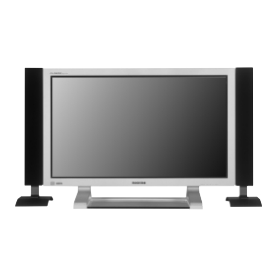
42” plasma pdp monitor
Hide thumbs
Also See for DP-42SM:
- Service manual (47 pages) ,
- User manual (51 pages) ,
- Instruction manual (11 pages)

Related Manuals for Daewoo DP-42SM


Summary of Contents for Daewoo DP-42SM
- Page 1 S/M NO. : DSP115BEF2 42” PLASMA PDP MONITOR CHASSIS : SP-115 MODEL : DP-42SM (FOR LG MODULE) DAEWOO ELECTRONICS Corp. http : //svc.dwe.co.kr Nov. 2003...
-
Page 2: Table Of Contents
Contents I. Parts with the exception of MODULE 1. Safety Precautions 2. Product Specification 2-1. SPECIFICATION 2-2. Available Input Signal 3. BLOCK DIAGRAM 4. Description Of Each BLOCK 4-1. A/V BLOCK 4-1-1. A/V BLOCK DIAGRAM 4-1-2. VIDEO PCB 4-1-3. JACK PCB 4-1-4. - Page 3 4-2-1. 4/7 or 3/7 of the screen doesn’t be shown 4-2-2. Screen doesn’t be shown as Data COF 4-2-3. It is generated unusual pattern of Data COF IC unit 4-2-4. Regular Stripe is generated about the quantity of one Data COF IC or more 4-2-5.
-
Page 4: Parts With The Exception Of Module
I. Parts with the exception of MODULE 1. Safety Precautions 1. Safety Precautions (1) When moving or laying down a PDP Set, at least two people must work. Avoid any impact towards the PDP Set. (2) Do not leave the broken PDP Set on for a long time. To prevent any further damages, after check the condition of the broken Set, make sure to turn the power (AC) off. -
Page 5: Product Specification
2. Product Specification 2-1. SPECIFICATION I T E M S P E C I F I C A T I O N REMARK 1. GENERAL 1-1. MODEL NO DSP-4280LVS(G, W) 1-2. CHASSIS NO SP-115 1-3. SCREEN SIZE 42 (16:9) 1-4. COUNTRY America 1-5. - Page 6 Product Specification I T E M S P E C I F I C A T I O N REMARK 4. OPTICAL 4-1. SCREEN SIZE 42 (106Cm) DIAGONAL 4-2. ASPECT RATIO 16:9 852(H)X480(V) 4-3. NUMBER OF PIXELS 16,700,000 COLOR( EACH 8BITS FOR RGB ) 4-4.
-
Page 7: Available Input Signal
Product Specification 2-2. Available Input Signal (1) PC Resolution H Freq. (KHz) V Freq. (Hz) Remark Patt No. 640x350 31.469 70.1 37.861 85.1 VESA 640x400 24.823 56.4 30.48 60.0 31.469 70.1 IBM (DOS) 37.861 85.1 VESA 640x480 31.469 59.9 66.7 Macintosh 37.861 72.8... - Page 8 Product Specification Resolution H Freq. (KHz) V Freq. (Hz) Remark Patt No. 1280X1024 46.433 43.4 VESA 63.981 60.0 VESA 70.66 66.5 74.88 70.0 78.125 72.0 HP & HITA 78.855 74.1 Sony & NEC 79.976 75.0 VESA 81.13 76.1 91.146 85.0 VESA 1600X1200 62.5...
-
Page 9: Block Diagram
3. BLOCK DIAGRAM... -
Page 10: Description Of Each Block
4. Description Of Each BLOCK 4-1. A/V BLOCK 4-1-1. A/V BLOCK DIAGRAM P601 P602 P603 RA1- RA1+ RB1- S_RESET V_MUTE RCLK1- RCLK1+ IC600 IC406 RD1- RD1+ PW171 DPTV-MVS RD2- RA2- RA2+ RB2- RB2+ RC2- VPEN1 RC2+ RCLK2- DIGITAL VPEN RCLK2+ RD2- RD2+ GBLKSLP... -
Page 11: Video Pcb
Description Of Each BLOCK 4-1-2.VIDEO PCB - PROCESS Various Signal (PC, COMPONENT, COMPOSITE ) to produce 24BIT DIGITAL output (1) IC and TP (1) IC400(UPD64083) -Using 3D COMBFILTER to separate COMPOSITE signal to Brightness Signal(Y) and Color Signal(C) *TP ( Input : COLOR BAR PATTERN ) A. - Page 12 Description Of Each BLOCK (3) IC406(DPTV-MVS) -A Scan Rate Converter which converts Interlace signal into Progressive signal A. VVS : VERTICAL SYNC (output of DPTV-MVS) B. VHS : HORIZONTAL SYNC (output of DPTV-MVS) C. VCLK : CLOCK (output of DPTV-MVS) -11-...
- Page 13 Description Of Each BLOCK (4) IC500(CXA3516R) -3-channel 8-bit 165MSPS A/D converter which process PC , DTV signal * TP A. GCOAST : COAST CONTOL Signal for PLL (input of CXA3516) B .GHS : HORIZONTAL SYNC for GRAPHIC (output of CXA3516) C.
- Page 14 Description Of Each BLOCK D. GFBK : SYNC for PLL (5) IC600(PW171) - Image processor IC A. DEN : DATA ENABLE (output of PW171) B. DHS : HORIZONTAL SYNC (output of PW171) -13-...
-
Page 15: Jack Pcb
Description Of Each BLOCK C.DVS : VERTICAL SYNC for DISPLAY (output of PW171) D. DCLKB : CLOCK for DISPLAY (output of PW171) 4-1-3. JACK PCB - Separate and process various VIDEO and AUDIO signal (1) IC706 (VIDEO /SYNC SELECTOR) - This chooses Y Cb/Pb Cr/Pr or RGB signal to output Y Cb/Pb Cr/Pr, to separate SYNC, and to perform SYNC COUNTER. -
Page 16: Key Pcb
Description Of Each BLOCK R_OUT(L_OUT) : AUDIO SIGNAL that goes into MSP3420 before AUDIO PROCESSING (4) IC701 .IC700 (TDA 7480) A. RIGHT(LEFT) :AMP input signal before 30dB amplification 4-1-4.KEY PCB - Input PCB using KEY 4-1-5.LED PCB - PCB for REMOCON CONTROL -15-... -
Page 17: Power Pcb
Description Of Each BLOCK 4-2. POWER PCB <Input requirements> Nominal Input Voltage : AC100V to AC240V (Variation Range - AC85V to AC276V) Single-Phase full wave Regulation Method : Transistor Switching Method Input Frequency : 50~60Hz (Variation range 45Hz to 66Hz) Inrush Current : 50A zero-peak max at AC264V Output Voltage is as follows. -
Page 18: Basic Congifuration
Description Of Each BLOCK Connector number Model name YMW025-10R YMW025-05R YMW025-04R Maker YEONHO YEONHO YEONHO The number of pins POWER (ON/OFF) V3 -17V V5 12V V3 17V Vstb number V4 5V * P2 is connected to P5 of Y-SUS PCB. P3 is connected to P1 of Z-SUS PCB. -
Page 19: Service Mode
5. SERVICE MODE 5-1. Entering SERVICE MODE Push UP MUTE DISPLAY MUTE BUTTON of Remote Controller to enter SERVICE adjustment MODE. 5-2. Check initial data of Video PCB (1) Check initial data of User Menu 1) Picture - Mode : Normal BRIGHTNESS : 35 CONTRAST : 47 COLOR : 32... -
Page 20: Description Of Service Mode Items
SERVICE MODE - Gain G : 64 - Gain B : 64 2) SAA 7118 - Sub BRT : 128 - Sub CONT : 50 - Sub CLR : 55 - Sub TINT : 0 - Sub SRP : 10 3) DPTV - Sub BRT : 61 - Sub CONT : 16... - Page 21 SERVICE MODE (1) SUB BRT : For BRIGHTNESS adjustment (fixed) (2) SUB CONT : For CONTRAST adjustment (fixed) (3) BIAS R : For R BIAS adjustment (Changeable) (4) BIAS G : For G BIAS adjustment (Changeable) (5) BIAS B : For B BIAS adjustment (fixed) (6) GAIN R : For R GAIN adjustment (Changeable) (7) GAIN G : For G GAIN adjustment (Changeable) (8) GAIN B : For B GAIN adjustment (fixed)
- Page 22 SERVICE MODE (2) TST PTRN MA : Cycled patterns from BK WH R G B by pressing volume up key (3) AT PWR : ON - Condition where turning AC power on, automatically turns the SET on. OFF - Condition where turning AC power on makes the Set STAND BY, and POWER of Remote-controller on turns the set on from STAND BY state.
- Page 23 SERVICE MODE (2) BWINV : Used to minimize Image Sticking Table Gamma Contents (ON/OFF) =2.2 ON : Inverting the original images.(in Digital image data, 0 1 , 1 =2.1 (default) * If Still images have been displayed for some =2.4 periods, this function can minimize Image sticking, by displaying it on BWINV mode for some times.
-
Page 24: Adjusting Method
6.Adjusting Method 6-1. Adjusting WHITE BALANCE 1) Apply 5 Step Gray Scale pattern to Video input terminal (MIK 7253S PATTERN NO.9) Fig. 2 5 Step Gray Scale Pattern 2) Check initial data of User Menu ( refer to 5-2 ) 3) To enter Service mode, press button up >... - Page 25 Adjusting Method Fig. 3 Power Connection and Voltage Adjustment Label 2. Vadd (ADDRESS Voltage) : DATA Input Voltage Measurement equipment : Digital Volt Meter (DC Volt mode) Adjusting TP : TP206 (See Fig. 4) Adjusting Location : RV204 (See Fig. 4) Optimum Adjusting Voltage : Voltage which is written in Label which is at upper right side of PDP Module.
-
Page 26: Software Upgrade Method
7.SOFTWARE UPGRADE Method 1. Connect the JACK PCB to the Video PCB. 2. Connect 9 PIN serial cable to the serial port of the computer. 3. Connect the opposite end of the serial cable to RS-232C port of Jack PCB. 4. - Page 27 SOFTWARE UPGRADE Method - Select the file (pwSDK.inf) you want to upgrade and Push Open(O) > button. 6. Select as above and push Next(N) > button. 7. Select Comm Port and Baud Rate and push Next(N) > button. -26-...
- Page 28 SOFTWARE UPGRADE Method 8. Upgrade process will be displayed. Turn on the ac power and then upgrade program will initiate the download. 9. When all files upgrade are complete, a window (below) will be opened. Push Finish button to complete the process. -27-...
-
Page 29: Main Pcb Trouble Diagnosis
8. Main PCB Trouble Diagnosis [NOTE] See II. PARTS of MODULE of this service manual for the trouble diagnosises concerned to MODULE with exception of VIDEO, JACK and POWER parts. 8-1. VIDEO & JACK PCB Trouble Diagnosis 1. Common checking process when No signal or No raster Check start 1. - Page 30 Main PCB Trouble Diagnosis S- VHS input : Check 24th pin of P502 (when COLOR BAR PATTERN). If above signal do not appear, JACK PCB has a trouble. (3) TP DECOE Check If DECOE signal do not appear, JACK PCB has a trouble. (cf.
- Page 31 Main PCB Trouble Diagnosis 4. When PC signal do not appear on screen (1) Input DTV or VIDEO signal and see if DTV or VIDEO signals shown on screen. -->If no signal, check TP DCLKB, DHS and DVS. -->If DCLKB, DHS and DVS signal do not appear, JACK PCB has a trouble. (2) Check 1st PIN (V SYNC), 2nd PIN (H SYNC) of P502 (when 800X600).
- Page 32 Main PCB Trouble Diagnosis 6. When Key does not operate Check start 1. Confirm AC connection. 2. Confirm Power S/W ON. Does LED next to Power 3. Check other PCBs S/W turn on in Red? 1. Check the connection to Video PCB. Does LED 2.
- Page 33 Main PCB Trouble Diagnosis 7. When Remote Controller does not operate Check start 1. Confirm AC connection. Does LED next to Power 2. Confirm Power S/W ON. S/W turn on in Red? 3. Check other PCBs. Check the Battery of Does Remote Controller Remote Controller operate?
-
Page 34: Power Pcb Trouble Diagnosis
Main PCB Trouble Diagnosis 8-2. POWER PCB Trouble Diagnosis Although Z-SUS / Y-SUS / SCAN / DATA COF (refer to II. PARTS of MODULE) are checked, but still the set does not operate, and then check if Trouble Symptoms of the following Power PCB appear. -
Page 35: Trouble Shooting
(2) This TROUBLE SHOOTING list only contains representative and simple PCB trouble diagnosis and Module Exchange method. Therefore, if you find Sets that are difficult to diagnose or to repair, contact Daewoo Electronics. (3) Basic TROUBLE SHOOTING procedure Check Trouble Symptoms... -
Page 36: Trouble Diagnosis And Repairing Method For Representative Symptoms
Trouble shooting <Symptom.4> No SOUND <Symptom.5> The Set does not operate normally. But, after turn off AC Power, if turn on again, it operates normally again. <Symptom.6> Remote Control or KEY does not operate <Symptom.7> POWER SHUT DOWN occur (refer to Service Manual I. 9-3 ) (3) Representative Symptoms caused by bad Connection between PCBs. - Page 37 Trouble shooting <3> Trouble Repairing Procedure - If no problem in Connection(VIDEO PCB ==>CONTROLLER PCB), replace VIDEO PCB AC PWR "OFF" BACK COVER "OPEN" POWER PCB's HIGH VOLTAGE SWITCH "OFF" (refer to Fig.4) AC PWR "ON" PWR "ON" with Remote Controller "SHUT DOWN"...
- Page 38 Trouble shooting AC PWR "OFF" HIGH VOLTAGE SWITCH of POWER PCB "OFF" (refer to Fig.4) Disconnect PWR Connectors of Z-SUS and Y-SUS AC PWR "ON" => PWR "ON" with Remote Controller "SHUT DOWN" occur? AC PWR "OFF" AC PWR "OFF" Disconnect AUDIO PWR Reconnect only PWR Connector Connector of JACK PCB...
- Page 39 Trouble shooting AC PWR "OFF" HIGH VOLTAGE SWITCH of POWER PCB "ON" (refer to Fig. 4) Disconnect PW R Connector s of Z-SUS and Y-SUS AC PWR "ON" => PWR "ON" with Rem ote Controller "SHUT DOWN" occur? AC PWR "OFF" POWER PCB is N.G.
-
Page 40: Assembly List
10. ASSEMBLY LIST PCB ASS Y NAME ASS Y CORD ASS Y DESCRIPTION VIDEO PCB AS PTVDMSG023 PCB VIDEO MANUAL AS JACK PCB AS PTJAMSG023 PCB JACK MANUAL AS MODULE PDP 4850M06410 PDP42V50011 MODULE POWER 4850M06310 PDD-422 CTRL PCB ASS Y 485AS01690 CTRL PCB AS(PDP42V50011 LG) Y-SUS PCB ASS Y... - Page 41 ASSEMBLY LIST COMPONENTS PICTURE REMARK 1) PDP MODULE (with F/SUPPORT) 2) VIDEO BOARD 3) JACK BOARD (with JACK PLATE and SHIDE CASE) 4) POWER BOARD -40-...
- Page 42 ASSEMBLY LIST COMPONENTS PICTURE REMARK 5) FRONT MASK 6) FILTER GLASS 7) BACK COVER -41-...
-
Page 43: Exploded View
11. EXPLODED VIEW -42-... -
Page 44: Parts Of Module
II. Parts of MODULE 1. Safety Precautions PDP Module is a display device to be divided into a Panel part and a Drive part. The Panel part consists of Electrodes, Phosphor, various dielectrics and gas, and the Drive part includes electronic circuitry and PCB. - Page 45 Safety Precautions (4) This product contains glass. The glass may break, causing injuries, if shock, vibration, heat, or distortion is applied to the product. (5) The temperature of the glass of the display may rise to 80 C or more depending on the conditions of use.
- Page 46 Safety Precautions (22) Do not cover or wrap the product with a cloth or other covering while power is supplied to the product. (23) Before turning on power to the product, check the wiring of the product and confirm that the supply voltage is within the rated voltage range.
-
Page 47: Formation And Specification Of Module
2. Formation and Specification of Module Fig. 8 Connection diagram External Cable Connection Connector Input Signal P1[Z SUS B/D] 5V, Va, Vs P5[Y SUS B/D] 5V, Vs P6[Y SUS B/D] P21, P31[CTRL B/D] Video Signal Part No. Description 6871QCH025A PWB(PCB) ASSY TMDS CTRL B/D ASSY 6871QCH029A PWB(PCB) ASSY... -
Page 48: Adjustment
3. Adjustment 3-1. Application Object This standard is applied to the PDP42V5#### PDP Module which is manufactured by the manufacturing team of PDP promotion department or elsewhere. 3-2. Notes (1) Without any special specification, the Module should be at the condition of preliminaries more than 10minutes before adjusting. - Page 49 Adjustment 3-3-2 Adjustment after assembling (PDP Module adjustment) (1) Setting up the initial voltage and adjusting the voltage wave form of Vsetup (2) Measuring the voltage Margin of Vs and deciding the voltage (3) Adjusting and checking the voltage of DC/DC pack (Vsetup, Vscw, -Ve, -Vy) (4) Adjusting the voltage wave form of Vset-down (5) Measuring the voltage Margin of Vset-up and deciding the voltage (6) Adjusting the wave form of final voltage...
- Page 50 Adjustment Fig. 9 Y Set-up Wave form Fig. 10 Z ramp Wave form 3-5. Adjustment after Assembling (PDP Module Adjustment) 3-5-1. Using Tools (1) Digital oscilloscope : More than 200MHz (2) DVM(Digital Multimeter): Fluke 87 or similar one (3) Signal generator: VG-825 or similar one (4) DC power supply - DC power supply for Vs (1) : Should be changeable more than 0-200V/ more than 10A - DC power supply for Va (1) : Should be changeable more than 0-100V/ more than 5A...
- Page 51 Adjustment 3-5-3. How to Adjust (1) Adjusting initial voltage wave form Check the voltage wave form like the mentioned way on the 3-4-3(How to adjust) and readjust the wave form when it is wrong. (2) Checking the DC/DC pack voltage - Convert the signal of signal generator to the 100% Full White signal - Connect the GND terminal of DVM to the GND of Y B/D and set the Plus terminal to the right up leg of R9 to check the -Ve voltage (-35 1V).
- Page 52 Adjustment (5) DC-DC Pack Voltage Set up Range Vsetup : 210V ~ 240V Vsc : 90V ~ 120V -Vy : -60V ~ -80V -Ve : -35V ~ -45V <Caution> (1) The power of the signal generator should be turned on before turning on the power of DC power supply.
-
Page 53: Trouble Shooting
4. Trouble Shooting 4-1. Checking for no Picture A screen doesn’t not display at all and condition of black pattern or power off. (1) Check whether the CTRL B/D LED(D1~D4) is turned on or not. (2) Check the power and signal cable of CTRL B/D. (3) X B/D, Y B/D, Z B/D is well plugged in. - Page 54 Trouble Shooting -53-...
-
Page 55: Hitch Diagnosis Following Display Condition
Trouble Shooting 4-2. Hitch Diagnosis Following Display Condition 4-2-1. 4/7 or 3/7 of the screen doesn’t be shown (1) Confirm the power connector of X B/D is well plugged in which is correspond to not showing screen. (2) Confirm the connector that is connected between CTRL B/D and X B/D correspond to not showing part. -
Page 56: It Is Generated Unusual Pattern Of Data Cof Ic Unit
Trouble Shooting * How to examine Data COF IC ANODE Pattern (GND) CATHOD Pattern and examine the Diode to the pure or reverse direction. Measure the third resistance value * How to examine Data COF IC 4-2-3. It Generates Unusual Pattern of Data COF IC unit (1) In case of generating unusual pattern of Data COF IC unit as below picture, there is problem in the check that is input into Data COF IC (2) In case of <case 1, 2, 3>... -
Page 57: Regular Stripe Is Generated About The Quantity Of One Data Cof Ic Or More
Trouble Shooting 4-2-4. Regular Stripe is Generated about the Quantity of one Data COF IC or more (1) In case of generating regular stripe about the quantity of one Data COF IC, there is problem at the output of output flatworm of X B/D. In case of generating regular stripe about the quantity of two Data COF ICs, that means the data which is conveyed from CTRL B/D is not conveyed well. -
Page 58: Regular Stripe Is Generated At Regular Internal On The Whole Screen
Trouble Shooting * Check a method of SCAN IC Change the Vpp Pin into ANODE and GND Pin into CATHOD and then test the Diode with forward or reverse direction. 4-2-6. The screen has a vertical line with regular gap. (A vertical stripe flash at especial color) (1) This is a problem about control B/D. -
Page 59: One Or More Stripe Is Generated On The Screen
Trouble Shooting 4-2-8. The screen has one or several vertical line (1) In this case, It isn’t a problem about controller B/D or XB/D. (2) It may cause followings. - It’s out of order a panel - Open or short of DATA COF FPC attached panel - It’s out of order a DATA COF attached panel (3) Replace Module. -
Page 60: Generated During Full-Black-Screen
Trouble Shooting 4-2-11. The screen displays other color partially on full white screen or happens discharge partially on full black screen. (1) Check the declination of Y B/D set up, set down wave. (2) Check the declination of Z B/D ramp wave. (3) Measure each output wave with oscilloscope (more than 200MHz) and compare the data with below figure data. -
Page 61: Block Diagram Of Module
5. Block Diagram of Module -60-...
Need help?
Do you have a question about the DP-42SM and is the answer not in the manual?
Questions and answers