Roland G-70 Service Notes
Hide thumbs
Also See for G-70:
- Owner's manual (261 pages) ,
- Addendum (19 pages) ,
- Specifications (4 pages)
Table of Contents
Advertisement
Quick Links
Feb.2005
TABLE OF CONTENTS
INFORMATION UPDATING MUSICAL DATA/OPERATIVE SYSTEM
CIRCUIT DIAGRAM (MAIN 7/14)
Copyright © 2005 by ROLAND CORPORATION
All rights reserved. No parts of this publication may be reproduced in any form whithout the written permission of
ROLAND CORPORATION.
2/3
14/18
SN00081
4
6
8
10
12
20
22
23
25
26
29
29
45
46
48
50
52
54
56
58
60
62
63
64
66
68
70
72
74
76
78
CIRCUIT DIAGRAM (CONTACT)
K6018563
SERVICE NOTES
Second edition
Issued by RES
Printed in Italy
G-70
80
82
83
84
86
88
90
92
92
94
96
98
100
102
104
106
109
110
112
114
116
118
120
122
124
126
128
130
130
130
132
134
Advertisement
Table of Contents

Related Manuals for Roland G-70


Summary of Contents for Roland G-70
-
Page 1: Table Of Contents
CIRCUIT DIAGRAM (MAIN 14/14) CIRCUIT BOARD (CONTACT) CIRCUIT BOARD (AUDIO) CIRCUIT DIAGRAM (CONTACT) Copyright © 2005 by ROLAND CORPORATION All rights reserved. No parts of this publication may be reproduced in any form whithout the written permission of ROLAND CORPORATION. SN00081... -
Page 2: Specifications
Feb.2005 SPECIFICATIONS ■ Keyboard: ■ Songs: 76-note synthesizer-action keys with aftertouch Real-time SMF player 4 programmable MARK & JUMP locations ■ Sound source: Song Cover 30 ALL Covers New WX sound engine 18 Drum Covers Max. polyphony 128 voices 24 Bass Covers Sounds 1596 tones in 16 families, Song Makeup Tools... - Page 3 Options grams, MIDI Sets, Play Lists, .txt PK-5A Dynamic MIDI Pedal, FC-7 Foot Controller, files MSA/MSD/MSE series floppy disks (Roland & third-party), RH-25/50/200 Headphones, DP-2 Pedal switch, DP-6 ■ Other functions: Pedal switch (piano type), BOSS FS 5U Foot switch,...
-
Page 4: Disassembly
Feb.2005 DISASSEMBLY... - Page 5 G-70...
-
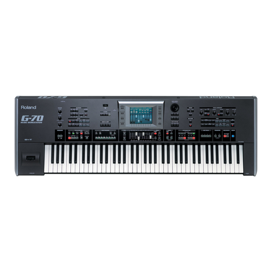
Page 6: Location Of Controls
Feb.2005 G-70 LOCATION OF CONTROLS... -
Page 7: Exploded View (Top)
Feb.2005 G-70 EXPLODED VIEW - TOP... -
Page 8: Exploded View (Bottom)
Feb.2005 G-70 EXPLODED VIEW - BOTTOM... -
Page 9: Keyboard Parts List
Feb.2005 G-70 KEYBOARD PARTS LIST 76-KEY KEYBOARD ASSY TP/8S-AT code 7699510001... -
Page 10: Parts List
7776418000 LEFT VARN. SIDE PANEL G-70 7776419000 VARN+SILKSCR. RIGHT END-BLOCK G-70 7776420000 VARN+SILKSCR. LEFT END-BLOCK G-70 7776423000 VARN. RIGHT SIDE PANEL CAP G-70 7776424000 VARN. LEFT SIDE PANEL CAP G-70 7776421000 VARN+SILKSCR. LCD COVER G-70 7776422000 MUSIC REST G-70 KNOB BUTTON... -
Page 11: Parts List
INVERTER PCB ASSY G-70 72898145 MAIN-BOARD G-70 Note : : Replacement MAIN-BOARD G-70 should be made on a unit basis. No replacements available for individual parts. Replacement only be a unit. We only supply: 02232245 RCA(PIN) JACK RCA(PIN) YKC21-3661 JK2 on main Board... - Page 12 Feb.2005 15119141 TRANSISTOR DTA-114 ESATP 15319107 TRANSISTOR 2SC-4116GR J5119106 TRANSISTOR 2SC-4213-A (TE85L) J5119107 TRANSISTOR 2SA-1586-GR (TE85R) DIODE 00129767 DIODE ZENER RD10M-T1B-B2 01897189 DIODE MA147-(TX) CHIP J5029118 LED DIODE SLR-343EBT3F (GREEN) J5029119 LED DIODE SLI-343URC3F (RED) 15019159RI DIODE 1N-4148 15339108 DIODE DA-204K 01121323 DIODE DA-204U...
- Page 13 7700424000 11P CABLE ASSY (12) -2C P.2 7776430000 11P CABLE ASSY (14) -2C P.2 JST D/R 7776425000 LEFT CTRL WIRING STRAND G-70 7776426001 RIGHT CTRL WIRING STRAND G-70 7776431000 BOTTOM WIRING STRAND G-70 K3468296 20P FLAT CABLE (40) -2C D/R...
- Page 14 D-BEAM CONTROLLER ESCT BLK K2248160 AC SOCKET HOLDER K253810302 FUSE WARNING LABEL K2268195 LCD VIBRATION-DAMPING (HLC30) G-70 K2248188 LCD ANTIDUST COVER (PL45) G-70 K2248189 ANTIDUST COVER PL45 (F/DRAWBAR) G-70 ACCESSORIES J3439155 CABLE CEE XVIIG-H05VVF2X1-C17W (only for 230V) 13499152RI CABLE BS/13/H05VV-F3G0 75-V...
- Page 15 G-70...
-
Page 16: Wiring Diagram
J3469159 AWG18 CBL (12) GREEN + FASTON (2) (Ground cables) 7776429000 10P CABLE ASSY (12) -2C P.2 JST D/R 7776425000 LEFT CTRL WIRING STRAND G-70 7700424000 11P CABLE ASSY (12) -2C P.2 7776426001 RIGHT CTRL WIRING STRAND G-70 7776430000 11P CABLE ASSY (14) -2C P.2 JST D/R... - Page 17 Userprg contains the files of the User Programs It is possible to access this structure by connecting the G-70 to a PC fitted with win98ME, Win2000/XP, MAC by means of a USB cable: Connect the G-70 to a PC by means of a USB cable.
-
Page 18: Updating Of Musical Data
Stereo Headphones UPDATING OF MUSICAL DATA ATTENTION!!! The data’s updating entails the loss of personal data contained in the G-70. There are two modes of updating the Data in the G-70: Mode 1: by means of a Card It is carried out by means of a card of at least 64 Mbytes and of a PCMCIA adaptor for this card. - Page 19 B. COPY THE MUSICAL DATA INTO THE CARD BY MEANS OF A PC Insert the card into a PC with the relative adaptor. Open the file previously created in the PC called for instance “G-70”, containing the data drawn from the CD ROM USB DRIVER Copy, selecting and drawing all the files from the PC to the card.
-
Page 20: Factory Reset
Open the folder previously created in the PC called “G-70” containing the data drawn CD ROM USB DRIVER. Copy, selecting and drawing all the files from the PC to the new G-70 virtual drive. ATTENTION!, before withdrawing the USB cable and switching off the instrument, disconnect the G-70 virtual drive from the PC by means of the appropriate function. -
Page 21: Updating Of The Operative System
MAY CAUSE THE COPY OF THE FILES TO BE INCOMPLETE. C. Updating the operative system Insert the card with its adaptor into the PCMCIA slot of the G-70. Switch on the instrument by keeping pressed the switch “DISK & MEDIA”. - Page 22 B: \ Update \\ G-70_ xxxxxx_xxxxxx_Build xx. sys Power Off And power On again The G-70 will make a deep check of the system file; should the file be correct, it will start the updating. A progression bar will show its status.
- Page 23 Wait until the instrument shows the video “Update All ” . Press the switch “USER PROGRAM 1”. The G-70 will make a deep check of the system file; should the file be correct, it will start the updating. A progression bar will show its status.
-
Page 24: Test Mode
PROCEDURE TO CHECK THE SOFTWARE VERSION WHEN SWITCHING ON Switch on the instrument keeping pressed the switch MUSIC ASSISTANCE; after a few seconds the display will show: **** VERSION **** Product : G-70 Version: xxx Date: xx.xx.xx Time: xx.xx.xx... - Page 25 Feb.2005 SECOND GROUP OF TESTS ( **** TEST MENU ( 2 / 2 ) ****) **** TEST MENU ( 2 / 2 ) **** 1. VIDEO OUTPUT 2. AUDIO TEST 3. KEYSCAN 7. PITCH CALIBRATION 8. SAVE SISTEM ON CARD Press LIST to scroll menu Pressing the switch LIST again, the display will show the first page of the main menu of the tests.
- Page 26 G-70 Note : if the switch test has been carried out previously, you may exit pressing MENU and EXIT at the same time. 2- LED COLOR CHECK Press the USER PROGRAM 2 button, the display shows: LED TEST ****** ******...
- Page 27 Feb.2005 3 - ADC Press the USER PROGRAM 3 button, the display shows: ****** ADC ****** Pbender : 0000 – 4000 - 7F7F 16’ : 0 – 255 Modul : 0 – 127 5 – 1 / 3’ : 0 – 255 A .Touch : 0 –...
- Page 28 Use the original pen (Touch Pen for PMA-5, code 00900545). Touch with the pen the Touch Screen corners in the middle of the “+” symbol following the numbering shown in the picture. When the G-70 recognizes the touch, the symbol “+” changes into “0”.
- Page 29 Feb.2005 NG. Calibration In case of a negative outcome of the calibration. Should the calibration fail, the operation has to be repeated from the start. Press EXIT to continue with the following check. 4.2 - X - Y TOUCH SCREEN TEST Press the USER PROGRAM 2 button, the display shows: **** TOUCHSCREEN **** Press Exit to Skip.
- Page 30 G-70 5.1- 2DD FLOPPY DISK CONTROLLER Press the USER PROGRAM 1 the display shows: **** FLOPPY CONTROLLER 2DD **** Insert a 2DD DISK, please….. Press EXIT to Skip. Insert a formatted diskette 2DD into the driver to carry out the test.
- Page 31 Feb.2005 5.2 2HD FLOPPY DISK CONTROLLER Press the USER PROGRAM 2 button to carry out the 2HD test. Use the same procedure stated in § 5.1 – FLOPPY DISK CONTROLLER 2DD To revert to the MASS STORAGE, press EXIT. Attention: Use only a formatted diskette 2DD and 2HD type. To revert to the Main Menu, press EXIT.
- Page 32 G-70 5.5 - FORMAT NAND FLASH Press the USER PROGRAM 5 button, the display shows: **** NAND FORMAT **** ** FORMAT OK ** Press EXIT to Skip To revert, press EXIT. 5.6 - USB Press the USER PROGRAM 6 button, the display shows: **** USB MASS STORAGE **** Connect USB cable to PC please…….
- Page 33 Remain in the MIDI Test video and connect the appropriate MIDI cables basing upon the above description. Leave the MIDI In/Out cable inserted into the G-70 and connect, by means of the MIDI cable, the MIDI Thru socket of the G-70 to the MIDI IN socket of second instrument.
- Page 34 5.Bars / Monoscope Press EXIT to Skip Remark: before carrying out the test, connect the G-70 VIDEO OUTPUT to the appropriate “PAL / NTSC Video Monitor” by means of a shielded cable. Pressing the USER PROGRAM 1 button, you will inter the PAL system test.
- Page 35 On the right side of the display appears the name of the latter. 2.2 - OUTPUT MAIN TEST Place the knob of the G-70’s MASTER VOLUME potentiometer in the CENTER before effecting the check of the level of the output signal on the L/R MAIN and DIRECT Outputs.
- Page 36 G-70 Press the USER PROGRAM 3 button again, you will hear an acoustic signal only on the right ( R ) OUT DIRECT basing upon the frequency selected by means of the User Prog. 1 button. Press the USER PROGRAM 2 button again, you will hear an acoustic signal on the right (...
- Page 37 Feb.2005 The display will show OK or ERROR. If the SRX card has been inserted into the appropriate slot located on the right side of the bottom cabinet, the test senses the type of card and its checksum, basing upon the schedule shown below: CHECKSUM SRX –...
-
Page 38: Bender Calibration
**** AUDIO OUTPUT ****) and press the USER PROGRAM 7 button, a METRONOME sound will be heard coming from the OUT Metronome output of the G-70. Action : Insert the headphones into the appropriate OUT Metronome socket located in the rear of the bottom cabinet. - Page 39 Release the Bender lever at the center and press the SET LIST SW button, the display will show: ** MODUL CALIBRATION ** Press the Modulation Lever To the back of the G-70 and press LIST SW Push the Bender lever completely to the center and press the SET LIST SW button. To confirm the calibration, the instrument exits the test, resets itself and reverts to the video of the main menu.
- Page 40 Release the Bender lever at the center and press the ASSIGN SW 1 button, the display will show: ** MODUL CALIBRATION ** Press the Modulation Lever To the back of the G-70 and press ASSIGN SW 1 Push the Bender lever completely to the center and press the ASSIGN SW 1 button. To confirm the calibration, the instrument exits the test, resets itself and reverts to the video of the main menu.
-
Page 41: Touch Screen Calibration
PMA-5, code #00900545). Touch with the pen the Touch screen corners in the middle of the “+” symbol following the numbering mentioned here under. When the G-70 recognizes the touching of the pen, the “+” symbol change in “0”. -- TOUCH SCREEN CALIBRATION -- Press this point The writing “PRESS THIS POINT”... - Page 42 G-70...
-
Page 43: Block Diagram
Feb.2005 G-70 BLOCK DIAGRAM Colour LCD DC-AC INVERTER EFFECT QVGA MOD1 DHE1105-5VE DBEAM CONTROLS Control Board 320x240 SW & LED PCMCIA Card Slot Video OUT ADC IN buffer 3.3V--->5V Harmonic Bars 8bit L- R PANEL BOARD SDRAM 16bit NOR Flash... -
Page 44: Circuit Board (Main)
Feb.2005 CIRCUIT BOARD (MAIN) - Page 45 G-70 CIRCUIT BOARD (MAIN)
-
Page 46: Circuit Diagram (Main 1/14)
Feb.2005 G-70 CIRCUIT DIAGRAM (MAIN 1/14) PWTP1 PWTP1 GRM39@ GRM39@ TESTLAND1R2S TESTLAND1R2S PWTP2 PWTP2 TESTLAND1R2S TESTLAND1R2S 2. 0 1.6k 1.6k RR0816@D RR0816@D 100/25 100/25 B10B-PH-K-S(PB-FREE) B10B-PH-K-S(PB-FREE) RV3-V@M-R RV3-V@M-R 02904945 SLF12565T@ SLF12565T@ PQ1CY1032ZP PQ1CY1032ZP PQ070XZ01ZP PQ070XZ01ZP VOUT 47uH 47uH VSOFT OADJ... -
Page 47: Circuit Diagram (Main 2/14)
Feb.2005 G-70 CIRCUIT DIAGRAM (MAIN 2/14) CA[0..24] CA[0..24] CD[0..31] CD[0..31] TESTLAND1R2S TESTLAND1R2S EXBE10C@J EXBE10C@J EVQ11A05R EVQ11A05R CA24 RPC05T@J RPC05T@J RPC05T@J RPC05T@J CA23 CA13 CD31 RA24 RA24 DQ15 GRM39@ GRM39@ CA22 CA12 CD30 XTAL2 A10/AP DQ14 CA21 CA11 CD29 EXBV8V@JV EXBV8V@JV... -
Page 48: Circuit Diagram (Main 3/14)
Feb.2005 G-70 CIRCUIT DIAGRAM (MAIN 3/14) CA[0..24] CA[0..24] Address Buffers XCS0 BA[0..24] XCSFLASH XCS0 IC14A IC14A XCS2 XCS0 XCSLCDC TC74VHC139FT TC74VHC139FT XCS2 IC15A IC15A XCS2 IC13A IC13A CA24 TC74VHC139FT TC74VHC139FT XCS3 HD74LV08AT HD74LV08AT CA23 CA24 XCS3 XCS5 CA23 XCS4 XCE1AB... -
Page 49: Circuit Diagram (Main 4/14)
Feb.2005 G-70 CIRCUIT DIAGRAM (MAIN 4/14) MA147-(TX) MA147-(TX) IC28A IC28A IC28C IC28C IC29C IC29C M5218AFP M5218AFP M5218AFP M5218AFP M5218AFP M5218AFP N2012Z601T02 N2012Z601T02 RPC05T@J RPC05T@J RPC05T@J RPC05T@J to AfterTouch PCB GRM39@ GRM39@ GRM39@ GRM39@ N2012Z601T02 N2012Z601T02 100p 100p 1.8k 1.8k B03B-PH-SM3-TB... -
Page 50: Circuit Diagram (Main 5/14)
Feb.2005 G-70 CIRCUIT DIAGRAM (MAIN 5/14) 820k 820k RPC05T@J RPC05T@J RPC05T@J RPC05T@J RPC05T@J RPC05T@J 2.2k 2.2k DBTP5 DBTP5 MA142WA-(TX) MA142WA-(TX) RPC05T@J RPC05T@J TESTLAND1R2S TESTLAND1R2S RPC05T@J RPC05T@J DBTP6 DBTP6 TESTLAND1R2S TESTLAND1R2S RPC05T@J RPC05T@J C100 C100 ECJ1V@ ECJ1V@ C101 C101 RPC05T@J RPC05T@J... -
Page 51: Circuit Diagram (Main 6/14)
Feb.2005 G-70 CIRCUIT DIAGRAM (MAIN 6/14) CIRCUIT DIAGRAM (MAIN 7/14) C136 C136 GRM31@ GRM31@ C135 C135 GRM39@ GRM39@ C134 C134 GRM39@ GRM39@ C133 C133 GRM39@ GRM39@ C132 C132 GRM39@ GRM39@ C131 C131 GRM39@ GRM39@ C130 C130 GRM39@ GRM39@ C129 C129... -
Page 52: Circuit Diagram (Main 8/14)
Feb.2005 G-70 CIRCUIT DIAGRAM (MAIN 8/14) WA[1..24] WA[1..24] to SRX EXP Board WD[0..15] GRM39@ GRM39@ C231 C231 IC50 IC50 GRM39@ GRM39@ HD74LV245ATELL HD74LV245ATELL CN12 CN12 XWCS7 C220 C220 EWA23 N1608Z@T01 N1608Z@T01 XWCS7 XWCS6 RA87 RA87 EWA22 N1608Z@T01 N1608Z@T01 XWCS6 XWCS5... -
Page 53: Circuit Diagram (Main 9/14)
Feb.2005 G-70 CIRCUIT DIAGRAM (MAIN 9/14) DA15 DA15 DA16 DA16 DA17 DA17 DA14 DA14 Io=100mA PWTP4 PWTP4 TESTLAND1R2S TESTLAND1R2S IC59 IC59 TA78L05F TA78L05F PWTP5 PWTP5 IC61B IC61B IC61A IC61A TESTLAND1R2S TESTLAND1R2S M5218AFP M5218AFP M5218AFP M5218AFP AD_BIAS C234 C234 33/25 33/25... -
Page 54: Circuit Diagram (Main 10/14)
Feb.2005 G-70 CIRCUIT DIAGRAM (MAIN 10/14) C280 C280 C281 C281 C282 C282 C283 C283 C284 C284 C285 C285 IC66 SED1356F0A IC66 SED1356F0A C286 C286 GRM31@ GRM31@ (S1D13506F00A200) C293 C293 BA[0..24] GRM31@ GRM31@ to Control Board BA[0..24] BA20 CN16 CN16 AB20... -
Page 55: Circuit Diagram (Main 11/14)
Feb.2005 G-70 CIRCUIT DIAGRAM (MAIN 11/14) GRM31@ GRM31@ C321 C321 GRM39@ GRM39@ C322 C322 GRM39@ GRM39@ C323 C323 C324 C324 GRM31@ GRM31@ GRM39@ GRM39@ C325 C325 C326 C326 GRM39@ GRM39@ GRM39@ GRM39@ C327 C327 C328 C328 GRM39@ GRM39@ BA[0..24] CN17 CN17 BA[0..24]... -
Page 56: Circuit Diagram (Main 12/14)
Feb.2005 G-70 CIRCUIT DIAGRAM (MAIN 12/14) BA[0..24] BA[0..24] BD[0..15] BD[0..15] C378 C378 Nand Flash ROM GRM39@ GRM39@ for USB storage IC79 IC79 TC74VHC175FT TC74VHC175FT Nor Flash ROM for system boot RA100 RA100 C379 C379 EXB28V@JX EXB28V@JX GRM31@ GRM31@ IC82 IC82... -
Page 57: Circuit Diagram (Main 13/14)
Feb.2005 G-70 CIRCUIT DIAGRAM (MAIN 13/14) BA[0..24] BA[0..24] C_D[0..15] PCMCIA Data Bus Buffer BD[0..15] C_A[0..10] CARD SLOT BD[0..15] GRM39@ GRM39@ CN23 CN23 Address Bus Buffer GRM39@ GRM39@ C394 C394 C393 C393 GRM39@ GRM39@ CARD_POWER C395 C395 IC92A IC92A RA104 RA104... -
Page 58: Circuit Diagram (Main 14/14)
Feb.2005 G-70 CIRCUIT DIAGRAM (MAIN 14/14) BA[0..24] BA[0..24] Test lands for debug BD[0..15] BD[0..15] BD15 BD15 TESTLAND1R2S BD15 TESTLAND1R2S BA15 BA15 TESTLAND1R2S BA15 TESTLAND1R2S BD14 BD14 TESTLAND1R2S BD14 TESTLAND1R2S BA14 BA14 TESTLAND1R2S BA14 TESTLAND1R2S BD13 BD13 TESTLAND1R2S BD13 TESTLAND1R2S BA13... -
Page 59: Circuit Board (Audio)
Feb.2005 G-70 CIRCUIT BOARD (AUDIO) View from component side... -
Page 60: Circuit Diagram (Audio 1/4)
Feb.2005 G-70 CIRCUIT DIAGRAM (AUDIO 1/4) R168 NIU R168 NIU MIC: Left (SW 2-3) LINE: Right (SW 2-1) SW1A SW1A 220p 220p 6.8k 6.8k SW1B SW1B SSSF11209K SSSF11209K SSSF11209K SSSF11209K DA204U DA204U 100k 100k 6.8k 6.8k 53014-0410 53014-0410 MICRTN to Harmony Board... -
Page 61: Circuit Diagram (Audio 2/4)
Feb.2005 CIRCUIT DIAGRAM (AUDIO 2/4) -
Page 62: Circuit Diagram (Audio 3/4)
G-70 CIRCUIT DIAGRAM (AUDIO 3/4) -
Page 63: Circuit Diagram (Audio 4/4)
Feb.2005 G-70 CIRCUIT DIAGRAM (AUDIO 4/4) C139 0.1 C139 0.1 C140 0.1 C140 0.1 C141 C141 +15V 10u/25 10u/25 C142 C142 +15V -15V C143 C143 C144 C144 100u/25 100u/25 -12V +12V MA147-(TX) MA147-(TX) RD10M_T1B_B2 RD10M_T1B_B2 R158 R158 R159 R159 From Power Supply Board... -
Page 64: Circuit Board (Harmony)
Feb.2005 G-70 CIRCUIT BOARD (HARMONY) View from component side... -
Page 65: Circuit Diagram (Harmony 1/2)
Feb.2005 G-70 CIRCUIT DIAGRAM (HARMONY 1/2) To Power Supply (CN10) IC11 IC11 EXCML20A@ EXCML20A@ TA7805F TA7805F 1.VA+ 2.AGND 3.VA- 100/16 100/16 4.AGND 100/16 100/16 5.VCC 6.VCC EXCML20A@ EXCML20A@ 7.DGND 8.DGND 9.DGND 100/16 100/16 53014-0910 53014-0910 10/16 10/16 5.6k 5.6k 330/6.3 330/6.3... -
Page 66: Circuit Diagram (Harmony 2/2)
Feb.2005 G-70 CIRCUIT DIAGRAM (HARMONY 2/2) D 3. 3 D 3. 3 C139 C139 C140 C140 C143 C143 C144 C144 10/16 10/16 10/16 10/16 10/16 10/16 10/16 10/16 C141 C141 C142 C142 10/16 10/16 10/16 10/16 10/16 10/16 10/16 10/16... -
Page 67: Circuit Board& Circuit Diagram (Inverter)
Feb.2005 G-70 CIRCUIT BOARD& CIRCUIT DIAGRAM (INVERTER) MOD1 MOD1 DHE1105-5VE DHE1105-5VE SM02(8R0)B-BHS-TB SM02(8R0)B-BHS-TB From Power To LCD unit Supply Board (CN4) 5045-04A 5045-04A 100nFC 100nFC 470uF16 470uF16 B2(4-2R3)B-XH-A B2(4-2R3)B-XH-A View from component side CIRCUIT BOARD (MIDI) View from component side... -
Page 68: Circuit Diagram (Midi)
Feb.2005 G-70 CIRCUIT DIAGRAM (MIDI) 1N4148 1N4148 1N4148 1N4148 DTA114ES DTA114ES ELKTR391CA ELKTR391CA SBT0460 SBT0460 1N4148 1N4148 1N4148 1N4148 ELKTR391CA ELKTR391CA FC-7 DTA114ES DTA114ES HOLD SWITCH 1N4148 1N4148 YKF51_5001 YKF51_5001 1N4148 1N4148 DTA114ES DTA114ES ELKTR391CA ELKTR391CA 1N4148 1N4148 SUST DTA114ES... -
Page 69: Circuit Board& Circuit Diagram (Lcd Control)
Feb.2005 G-70 CIRCUIT BOARD& CIRCUIT DIAGRAM (LCD CONTROL) DA204K DA204K B15B_PH_K_S B15B_PH_K_S 20FLT_SM1_TB 20FLT_SM1_TB 2SC4116GR 2SC4116GR 2SC4116GR 2SC4116GR DA204K DA204K DISP_ON +5VD B10B-PH-K-S B10B-PH-K-S DGND From Mainboard XRES LCDCONT View from component side GNDCNT0 (CN16) GNDCNT1 52043_0410 52043_0410 To LCD unit... -
Page 70: Circuit Board (Right Control)
Feb.2005 G-70 CIRCUIT BOARD (RIGHT CONTROL) View from component side... -
Page 71: Circuit Diagram (Right Control 1/4)
Feb.2005 G-70 CIRCUIT DIAGRAM (RIGHT CONTROL 1/4) ALL DIODES ARE 1N4148. SWITCHES ARE EVQPAE05R VLED 74HC138 74HC138 IC15 IC15 RN2227 RN2227 VLED FIND SONG TA UP1 UP 1 MULTI FX FIND SONG TA UP1 UP 1 MULTI FX 1N4148 1N4148... -
Page 72: Circuit Diagram (Right Control 2/4)
Feb.2005 G-70 CIRCUIT DIAGRAM (RIGHT CONTROL 2/4) ALL DIODES ARE 1N4148. VLED SWITCHES ARE EVQPAE05R 74HC138 74HC138 RN2227 RN2227 VLED PIANO E.PIANO CHR PERC ORGAN PIANO E.PIANO CHR PERC ORGAN 1N4148 1N4148 1N4148 1N4148 1N4148 1N4148 1N4148 1N4148 SW33 SW33... -
Page 73: Circuit Diagram (Right Control 3/4)
Feb.2005 G-70 CIRCUIT DIAGRAM (RIGHT CONTROL 3/4) SLI-343URC3F SLI-343URC3F D123 D123 SW65 SW65 SW66 SW66 SW67 SW67 SW68 SW68 PEDAL_SUSTAIN EVQ-PAE 05 R EVQ-PAE 05 R EVQ-PAE 05 R EVQ-PAE 05 R EVQ-PAE 05 R EVQ-PAE 05 R EVQ-PAE 05 R... -
Page 74: Circuit Diagram (Right Control 4/4)
Feb.2005 G-70 CIRCUIT DIAGRAM (RIGHT CONTROL 4/4) IC8C +12V M5218AP VLED 100nF 33uF 100nF 100uF 470uF 100nF 5VREF 33uF SCL1 SDA1 -12V 5VREF SDA1 ELKTR391CA SCL1 TO MAIN BOARD SDA0 SCL0 TO MIDI BOARD (CN20) (CN2) SCL0 S07B-PH-K-S 53015-0510 IC8A... -
Page 75: Circuit Board & Circuit Diagram (Right Control Lcd)
Feb.2005 CIRCUIT BOARD & CIRCUIT DIAGRAM (RIGHT CONTROL LCD) View from component side SLR-343EBT3F SLR-343EBT3F SLR-343EBT3F SLR-343EBT3F SLR-343EBT3F SLR-343EBT3F SLI-343URC3F SLI-343URC3F green green green green green green EVQ-PAE 05 R EVQ-PAE 05 R EVQ-PAE 05 R EVQ-PAE 05 R EVQ-PAE 05 R EVQ-PAE 05 R EVQ-PAE 05 R EVQ-PAE 05 R... -
Page 76: Circuit Board & Circuit Diagram (Left Control Lcd)
G-70 CIRCUIT BOARD & CIRCUIT DIAGRAM (LEFT CONTROL LCD) View from component side L-934MBDL L-934MBDL SLR-343EBT3F SLR-343EBT3F SLR-343EBT3F SLR-343EBT3F SLR-343EBT3F SLR-343EBT3F green green green green green green EVQ-PAE 05 R EVQ-PAE 05 R EVQ-PAE 05 R EVQ-PAE 05 R EVQ-PAE 05 R... -
Page 77: Circuit Board (Left Control)
Feb.2005 G-70 CIRCUIT BOARD (LEFT CONTROL) View from component side... -
Page 78: Circuit Diagram (Left Control 1/6)
Feb.2005 G-70 CIRCUIT DIAGRAM (LEFT CONTROL 1/6) 5VREF 100nF BALANCE MODULATION +12V R3 100 RK11K113003SA BENDER -12V UNIT IC1A M5218AP +12V 100nF 100nF BZX55C 5V1 IC1C M5218AP 100nF 33uF S4B-PH-K-S -12V -12V 100nF -12V 100nF BEND BENDER IC1B M5218AP 100nF... -
Page 79: Circuit Diagram (Left Control 2/6)
Feb.2005 G-70 CIRCUIT DIAGRAM (LEFT CONTROL 2/6) ALL DIODES ARE 1N4148. SWITCHES ARE EVQPAE05R VLED IC14 IC14 74HC138 74HC138 RN2227 RN2227 VLED PLAY LIST NEXT SONG MINUS 1 16TRK PLAY LIST NEXT SONG MINUS 1 16TRK 1N4148 1N4148 1N4148 1N4148... -
Page 80: Circuit Diagram (Left Control 3/6)
Feb.2005 G-70 CIRCUIT DIAGRAM (LEFT CONTROL 3/6) ALL DIODES ARE 1N4148. SWITCHES ARE EVQPAE05R VLED IC15 IC15 74HC138 74HC138 RN2227 RN2227 US PRG 1 VOLUME US PRG 1 VOLUME VLED 1N4148 1N4148 1N4148 1N4148 SW32 SW32 SW33 SW33 ID=1 green... -
Page 81: Circuit Diagram (Left Control 4/6)
Feb.2005 G-70 CIRCUIT DIAGRAM (LEFT CONTROL 4/6) SLR-343EBT3F SLR-343EBT3F SLR-343EBT3F SLR-343EBT3F SLR-343EBT3F SLR-343EBT3F SLR-343EBT3F SLR-343EBT3F SLR-343EBT3F SLR-343EBT3F SLR-343EBT3F SLR-343EBT3F SLR-343EBT3F SLR-343EBT3F green green green green green green green green green green green green green green SW42 SW42 SW43 SW43 SW44... -
Page 82: Circuit Diagram (Left Control 5/6)
Feb.2005 G-70 CIRCUIT DIAGRAM (LEFT CONTROL 5/6) SLI-343URC3F SLI-343URC3F SLI-343URC3F SLI-343URC3F SLI-343URC3F SLI-343URC3F SLI-343URC3F SLI-343URC3F SLI-343URC3F SLI-343URC3F SLI-343URC3F SLI-343URC3F SLI-343URC3F SLI-343URC3F SW49 SW49 SW50 SW50 SW51 SW51 SW52 SW52 SW53 SW53 SW54 SW54 SW55 SW55 EVQ-PAE 05 R EVQ-PAE 05 R... -
Page 83: Circuit Diagram (Left Control 6/6)
Feb.2005 G-70 CIRCUIT DIAGRAM (LEFT CONTROL 6/6) SW56 SW56 SW57 SW57 ID=6 100nF 100nF 100uF 100uF IC12 IC12 R104 R104 R105 R105 EVQ-PAE 05 R EVQ-PAE 05 R EVQ-PAE 05 R EVQ-PAE 05 R M62320P M62320P PLAY/STOP START/STOP SDA1 SDA1... -
Page 84: Circuit Board & Circuit Diagram (Harmonic Bar)
Feb.2005 G-70 CIRCUIT BOARD & CIRCUIT DIAGRAM (HARMONIC BAR) View from component side 33uF 33uF 33uF 33uF 5VREF 5VREF 100nF 100nF 100nF 100nF 33uF NIU 33uF NIU 5VREF 100nF 100nF 5-1/3 2-2/3' 1-3/5' 1-1/3' 5VREF 5-1/3 TO RIGHT PANEL 2-2/3'... -
Page 85: Circuit Board & Circuit Diagram (Power)
Feb.2005 G-70 CIRCUIT BOARD & CIRCUIT DIAGRAM (POWER) uA7812CV uA7812CV B10B-PH-K-S B10B-PH-K-S +12V 47uF25 47uF25 TO MAIN BOARD 100uF16 100uF16 100nFC 100nFC 100nFC 100nFC A.GND (CN 1) 47uF25 47uF25 100nFC 100nFC 100nFC 100nFC JUMPER@ JUMPER@ 100uF16 100uF16 B11B-PH-K-S B11B-PH-K-S -12V... -
Page 86: Circuit Board & Circuit Diagram (Srx)
Feb.2005 G-70 CIRCUIT BOARD & CIRCUIT DIAGRAM (SRX) D+3.3V TX25-80P-6ST-E1 TX25-80P-6ST-E1 32FE-BT-VK-N 32FE-BT-VK-N D+3.3V 10uF16 10uF16 EWA23 EWA22 EWA20 EWA21 EWA19 EWA18 EWA9 IC2C IC2C EWA8 TC74VHC139F TC74VHC139F EWA10 EWA23 EWA7 EWA22 EWA11 EWA21 EWA6 EWA20 EWA12 EWA19 EWA5 EWA24... -
Page 87: Circuit Board & Circuit Diagram (Phones)
Feb.2005 G-70 CIRCUIT BOARD & CIRCUIT DIAGRAM (PHONES) L1=L2=BL02RN2-R62T2 100nFC 100nFC YKB21_5006 YKB21_5006 100nFC 100nFC 100nFC 100nFC 100nFC 100nFC 53014-0610 53014-0610 View from component side CIRCUIT BOARD & CIRCUIT DIAGRAM (ENCODER) TO RIGHT PANEL ENC1 ENC1 ENCA (CN8) ENCB 53015-0510... -
Page 88: Circuit Board (Contact)
Feb.2005 G-70 CIRCUIT BOARD (CONTACT w/RUBBER View fromsolder side... - Page 89 Feb.2005 G-70 CIRCUIT DIAGRAM (CONTACT BOARD) SW10 SW11 SW12 SW13 SW14 SW15 SW16 SW17 SW18 SW19 SW20 SW21 SW22 SW23 SW24 SW25 SW26 SW27 SW28 SW29 SW30 SW31 SW32 ampc1_2716p LEFT CONTACT PCB ASSY SW33 SW34 SW35 SW36 SW37 SW38...
Need help?
Do you have a question about the G-70 and is the answer not in the manual?
Questions and answers