Table of Contents
Advertisement
SERVICE MANUAL
Main Section
I Specifications
I Preparation for Servicing
I Adjustment Procedures
I Schematic Diagrams
I CBA's
I Exploded views
I Parts List
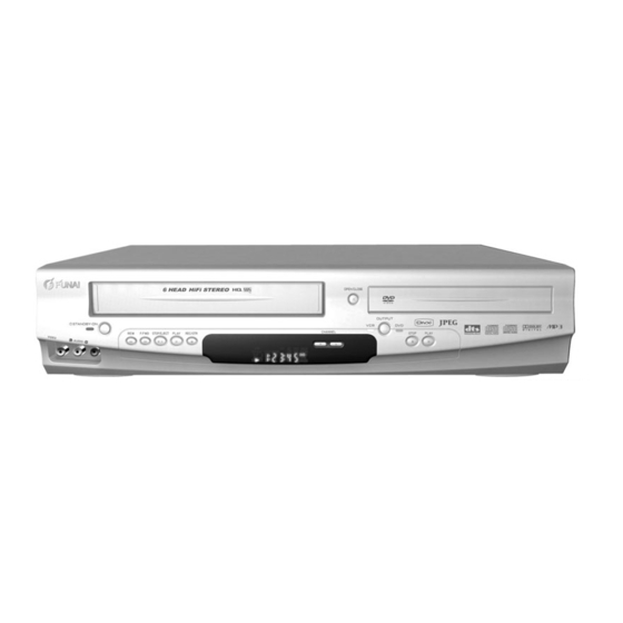
VIDEO CASSETTE RECORDER
DCVR-7830D DBVR-7730D
DVD PLAYER &
DPVR-7630D
When servicing the deck
mechanism, refer to MK14 Deck
Mechanism Section.
Deck Mechanism Part No.:
N25E0FL
PAL
PAL
SECAM
Advertisement
Table of Contents

Related Manuals for FUNAI DPVR-7630D


Summary of Contents for FUNAI DPVR-7630D
-
Page 1: Dvd Player
MK14 Deck I Preparation for Servicing Mechanism Section. I Adjustment Procedures I Schematic Diagrams Deck Mechanism Part No.: I CBA’s I Exploded views N25E0FL I Parts List DVD PLAYER & VIDEO CASSETTE RECORDER DPVR-7630D DCVR-7830D DBVR-7730D SECAM... -
Page 2: Table Of Contents
MAIN SECTION DVD PLAYER & VIDEO CASSETTE RECORDER DPVR-7630D/DCVR-7830D/DBVR-7730D Main Section I Specifications I Preparation for Servicing I Adjustment Procedures I Schematic Diagrams I CBA’s I Exploded Views I Parts List TABLE OF CONTENTS Specifications ............... . . 1-1-1 Laser Beam Safety Precautions . -
Page 3: Specifications
SPECIFICATIONS < VCR Section > Description Unit Minimum Nominal Maximum Remark 1. Video 1-1. Video Output (PB) Vp-p SP Mode 1-2. Video Output (R/P) Vp-p SP Mode, 1-3. Video S/N Y (R/P) W/O Burst 1-4. Video Color S/N AM (R/P) SP Mode 1-5. - Page 4 < DVD Section > ITEM CONDITIONS UNIT NOMINAL LIMIT 75 Ω load 1. Video Output ± 0.1 2. Optical Digital Out 3. Audio (PCM) 1 kHz 0 dB, 47k Ω load 3-1. Output Level Vrms 47k Ω load 3-2. S/N 3-3.
-
Page 5: Laser Beam Safety Precautions
LASER BEAM SAFETY PRECAUTIONS This DVD player uses a pickup that emits a laser beam. Do not look directly at the laser beam coming from the pickup or allow it to strike against your skin. The laser beam is emitted from the location shown in the figure. When checking the laser diode, be sure to keep your eyes at least 30 cm away from the pickup lens when the diode is turned on. -
Page 6: Important Safety Precautions
IMPORTANT SAFETY PRECAUTIONS Product Safety Notice K. Crimp type wire connector The power transformer uses crimp type connectors Some electrical and mechanical parts have special which connect the power cord and the primary side safety-related characteristics which are often not evi- of the transformer. -
Page 7: Safety Check After Servicing
Safety Check after Servicing Examine the area surrounding the repaired location for damage or deterioration. Observe that screws, Chassis or Secondary Conductor parts, and wires have been returned to their original positions. Afterwards, do the following tests and con- Primary Circuit firm the specified values to verify compliance with safety standards. -
Page 8: Standard Notes For Servicing
STANDARD NOTES FOR SERVICING Circuit Board Indications Pb (Lead) Free Solder When soldering, be sure to use the Pb free solder. 1. The output pin of the 3 pin Regulator ICs is indi- cated as shown. How to Remove / Install Flat Pack-IC Top View Bottom View 1. - Page 9 3. The flat pack-IC on the CBA is affixed with glue, so With Soldering Iron: be careful not to break or damage the foil of each (1) Using desoldering braid, remove the solder from all pin or the solder lands under the IC when removing pins of the flat pack-IC.
- Page 10 2. Installation (4) Bottom of the flat pack-IC is fixed with glue to the CBA; when removing entire flat pack-IC, first apply (1) Using desoldering braid, remove the solder from soldering iron to center of the flat pack-IC and heat the foil of each pin of the flat pack-IC on the CBA up.
- Page 11 Instructions for Handling Semi-conductors Electrostatic breakdown of the semi-conductors may occur due to a potential difference caused by electro- static charge during unpacking or repair work. 1. Ground for Human Body Be sure to wear a grounding band (1MΩ) that is prop- erly grounded to remove any static electricity that may be charged on the body.
-
Page 12: Preparation For Servicing
PREPARATION FOR SERVICING How to Enter the Service Mode About Optical Sensors Caution: An optical sensor system is used for the Tape Start and End Sensors on this equipment. Carefully read and follow the instructions below. Otherwise the unit may operate erratically. What to do for preparation Insert a tape into the Deck Mechanism Assembly and press the PLAY button. -
Page 13: Cabinet Disassembly Instructions
CABINET DISASSEMBLY INSTRUCTIONS 1. Disassembly Flowchart REMOVAL This flowchart indicates the disassembly steps to gain REMOVE/*UNHOOK/ LOC. PART Fig. access to item(s) to be serviced. When reassembling, UNLOCK/RELEASE/ Note follow the steps in reverse order. Bend, route, and UNPLUG/DESOLDER dress the cables as they were originally. 5(S-8), 2(S-9), [1] Top Case (S-10A),... - Page 14 Reference Notes CAUTION 1: Locking Tabs (L-1) and (L-2) are fragile. Be careful not to break them. (S-1) (S-1) 1-1. Release three Locking Tabs (L-1). [1] Top Case 1-2. Release three Locking Tabs (L-2), then remove the Front Assembly. CAUTION 2: Electrostatic breakdown of the laser (S-1) diode in the optical system block may occur as a potential difference caused by electrostatic charge...
- Page 15 CN401 (S-3) CN601 (S-9) (S-8) (S-3) (S-8) [4] DVD Mechanism (S-9) Assembly (S-3) (S-4) [5] Partition Plate (S-10B) (S-5) (S-6) (S-8) CN501 [DBVR-7730D [9] VCR Chassis Unit [7] Loader only] (S-10A) Holder [6] Power Supply CBA (L-3) Fig. D5 Fig. D3 (S-7) (S-7) [8] DVD Main...
- Page 16 Cylinder Assembly FE Head ACE Head Assembly [10] Deck Assembly SW507 Lead with blue stripe Lead with blue stripe LD-SW Desolder [14] Jack-A CBA (S-11) (S-13) [13] Main CBA [12] Power [10] Deck Assembly (S-13) SW CBA Cam Gear (DBVR-7730D only) Desolder (S-11) Hole...
- Page 17 HOW TO EJECT MANUALLY 1. Remove the Top Case, Front Assembly and Top Bracket. 2. Remove four Screws (S-3) in Fig. D3. Do not disconnect connectors. 3. While lifting up the DVD Mechanism, rotate the roulette in the direction of the arrow as shown below.
-
Page 18: Electrical Adjustment Instructions
Purpose: To determine the Head Switching position during When the “0: FUNC SET” value is not “038D” playback. (DPVR-7630D) or “038F” (DCVR-7830D) or “038C” (DBVR-7730D): Symptom of Misadjustment: 1. To enter the initial function setting mode, press [0] May cause Head Switching noise or vertical jitter button on the remote control. -
Page 19: How To Initialize The Dvd Player & Vcr
HOW TO INITIALIZE THE DVD PLAYER & VCR To put the program back at the factory-default, initialize the DVD player & VCR as the following procedure. < DVD Section > 1. Press [DVD], [1], [2], [3], [4], and [DISPLAY] buttons on the remote control unit in that order. Fig. -
Page 20: Firmware Renewal Mode
FIRMWARE RENEWAL MODE 1. Turn the power on and remove the disc on the tray. 5. After programming is finished, the tray opens automatically. Fig. e appears on the screen and 2. To put the DVD player into version up mode, press the checksum in (*2) of Fig. - Page 21 10. Press [CLEAR] button on the remote control unit. Fig. h appears on the screen. " ******* " differs depending on the models. MODEL : ******* Version : *.** Region : * EEPROM CLEAR : OK EEPROM CLEAR : CLEAR EXIT: POWER Fig.
-
Page 22: Function Indicator Symbols
FUNCTION INDICATOR SYMBOLS Note: If a mechanical malfunction occurs, the power is turned off. When the power comes on again after that by pressing [STANDBY-ON] button, an error message is displayed on the TV screen for 5 seconds. MODE INDICATOR ACTIVE When reel or capstan mechanism is not “A R”... -
Page 23: Block Diagrams
BLOCK DIAGRAMS <VCR SECTION> Servo / System Control Block Diagram E8B05BLS 1-11-1... - Page 24 Video Block Diagram E8B05BLV 1-11-2...
- Page 25 Audio Block Diagram E8B05BLA 1-11-3...
- Page 26 Hi-Fi Audio Block Diagram E8B05BLH 1-11-4...
- Page 27 Power Supply Block Diagram E8B05BLP 1-11-5...
- Page 28 BLOCK DIAGRAMS <DVD SECTION> DVD System Control / Servo Block Diagram E8B05BLSD 1-11-6...
- Page 29 Digital Signal Process Block Diagram E8B05BLD 1-11-7...
- Page 30 DVD Video / Audio Block Diagram 1-11-8 E8B05BLVD...
-
Page 31: Schematic Diagrams / Cba's And Test Points
SCHEMATIC DIAGRAMS / CBA’S AND TEST POINTS Standard Notes WARNING Many electrical and mechanical parts in this chassis have special characteristics. These characteristics often pass unnoticed and the protection afforded by them cannot necessarily be obtained by using replacement components rated for higher voltage, wattage, etc. - Page 32 LIST OF CAUTION, NOTES, AND SYMBOLS USED IN THE SCHEMATIC DIAGRAMS ON THE FOLLOWING PAGES: 1. CAUTION: FOR CONTINUED PROTECTION AGAINST FIRE HAZARD, REPLACE ONLY WITH THE SAME TYPE FUSE. 2. CAUTION: Fixed Voltage (or Auto voltage selectable) power supply circuit is used in this unit. If Main Fuse (F1001) is blown, first check to see that all components in the power supply circuit are not defec- tive before you connect the AC plug to the AC power supply.
- Page 33 Main 1/9 Schematic Diagram < VCR Section > Comparison Chart of Models and Marks MODEL MARK DPVR-7630D DCVR-7830D DBVR-7730D 1-12-3 E8B05SCM1...
- Page 34 Main 2/9, Sensor & Power SW Schematic Diagram < VCR Section > IC611 MATRIX CHART SACD PSCAN REPEAT SACD PSCAN REPEAT TITLE GROUP GROUP TITLE HD VCD Comparison Chart of Models and Marks MODEL MARK DPVR-7630D DCVR-7830D DBVR-7730D 1-12-4 E8B05SCM2...
- Page 35 Main 3/9 Schematic Diagram < VCR Section > Comparison Chart of Models and Marks MODEL MARK DPVR-7630D DCVR-7830D DBVR-7730D 1-12-5 E8B05SCM3...
- Page 36 Main 4/9 Schematic Diagram < VCR Section > 1-12-6 E8B05SCM4...
- Page 37 Main 5/9 Schematic Diagram < VCR Section > 1-12-7 E8B05SCM5...
- Page 38 Main 6/9 Schematic Diagram < VCR Section > 1-12-8 E8B05SCM6...
- Page 39 Main 7/9 & DVD Open/Close Schematic Diagram < VCR Section > 1-12-9 E8B05SCM7...
- Page 40 Main 8/9 Schematic Diagram < VCR Section > 1-12-10 E8B05SCM8...
- Page 41 Main 9/9 Schematic Diagram < VCR Section > ( B ) Comparison Chart of Models and Marks MODEL MARK DPVR-7630D DCVR-7830D DBVR-7730D 1-12-11 E8B06SCM9...
- Page 42 Power Supply & Junction Schematic Diagram < VCR Section > CAUTION ! CAUTION ! NOTE: Fixed voltage (or Auto voltage selectable) power supply circuit is used in this unit. For continued protection against fire hazard, The voltage for parts in hot circuit is measured using If Main Fuse (F1001) is blown , check to see that all components in the power supply hot GND as a common terminal.
- Page 43 Jack - A Schematic Diagram < VCR Section > E8B05SCJ 1-12-13...
- Page 44 AFV Schematic Diagram < VCR Section > Comparison Chart of Models and Marks MODEL MARK DPVR-7630D DCVR-7830D DBVR-7730D E8B05SCAFV 1-12-14...
- Page 45 DVD Main 1/3 Schematic Diagram < DVD Section > 1 NOTE: Either IC461 or IC462 is used for DVD MAIN CBA UNIT. 1-12-15 E8B05SCD1...
- Page 46 DVD Main 2/3 Schematic Diagram < DVD Section > 1-12-16 E8B05SCD2...
- Page 47 IC101 Voltage Chart ~ : Voltage is not consistent ----- : Not used Unit : Volts PIN.NO PLAY STOP PIN.NO PLAY STOP PIN.NO PLAY STOP PIN.NO PLAY STOP PIN.NO PLAY STOP PIN.NO PLAY STOP PIN.NO PLAY STOP PIN.NO PLAY STOP ----- ----- -----...
- Page 48 DVD Main 3/3 Schematic Diagram < DVD Section > 1-12-18 E8B05SCD3...
- Page 49 Main CBA Top View Sensor CBA Top View BHF300F01012A TP751 TP301 BHF300F01012B V-OUT C-PB TP504 RF-SW TP501 S-INH TP503 1-12-19 BE8B00F01013A...
- Page 50 Main CBA Bottom View PIN 6 OF IC1403 PIN 16 OF CN1601 PIN 14 OF CN1601 PIN 12 OF CN1601 PIN 10 OF CN1601 PIN 8 OF CN1601 1-12-20 BE8B00F01013A...
- Page 51 AFV CBA Top View AFV CBA Bottom View Power SW CBA Models and Marks Top View ( C ) Bottom View ( C ) MODEL MARK DPVR-7630D DCVR-7830D DBVR-7730D BE8B00F01013B DVD Open/Close DVD Open/Close CBA Top View CBA Bottom View...
- Page 52 Power Supply CBA Top View Power Supply CBA Bottom View Because a hot chassis ground is present in the power CAUTION ! CAUTION ! supply circut, an isolation transformer must be used. For continued protection against fire hazard, Fixed voltage (or Auto voltage selectable) power supply circuit is used in this unit. replace only with the same type fuse.
-
Page 53: Waveforms
WAVEFORMS NOTE: Input COLOR BAR SIGNAL (WITH 1KHz AUDIO SIGNAL) TP301 UPPER TP504 Pin 8 of CN1601 Pin 12 of CN1601 LOWER C-PB 0.2V DVD-AUDIO(L) 0.5ms RF-SW VIDEO-Y 0.2V 20µs TP751 UPPER TP504 Pin 10 of CN1601 Pin 14 of CN1601 LOWER V-OUT 0.5V... -
Page 54: Wiring Diagram < Vcr Section
WIRING DIAGRAM < VCR SECTION > 1-14-1 E8B05WI... -
Page 55: Wiring Diagram < Dvd Section
WIRING DIAGRAM < DVD SECTION > 1-14-2 E8B05WID... -
Page 56: Ic Pin Function Descriptions
Function Name Level Comparison Chart of Models and Marks Video Head OUT RF-SW Switching Model Mark Pulse DPVR-7630D HiFi Audio DCVR-7830D OUT Hi-Fi-H- Head DBVR-7730D Switching IC501( SERVO / SYSTEM CONTROL IC ) Pulse Not Used “H” ≥ 4.5V, “L” ≤ 1.0V... - Page 57 Mark IN/ Signal Active Mark IN/ Signal Active Function Function Name Level Name Level Clock Select Capstan Power IN CLKSEL OUT C-POW- (GND) Switching Signal Clock Input for IN OSCin letter size Power On OUT P-ON-H Signal at High Clock Output OUT OSCout for letter size OUT DRV-...
- Page 58 IC612 ( FIP DRIVER ) Mark IN/ Signal Active Function Name Level Signal Name Function AMPVRE V-Ref for CTL Name F OUT FP-CLK Clock Input AMPVRE V-Ref for CTL F in FP-STB Serial Interface Strobe P80/C P80/C Terminal Not Used Playback/ CTL (-) Record Control...
-
Page 59: Lead Identifications
LEAD IDENTIFICATIONS KRA103M-AT/P 2SA1015-GR(TE2 F T) MID-32A22F 2SK3566 KRC103M-AT/P 2SA1020-Y(TE6 F M) PT204-6B-12 KTA1266-GR-AT/P 2SA1815-(BL,GR,Y)(TE2 F T) KTA1267-(GR,Y)-AT/P 2SC2120-Y(TE2 F T) KTC3199-(BL,GR,Y)-AT/P 2SC3266-Y(TPE2 F) RN2204(TE4 F T) KTA1281Y-AT/P KTC3203-Y-AT/P KTC3205-Y-AT/P G D S E C B E C B KIA4558P/P KRC103S-RTK/P FMG4A T148 BR24L02F-WE2... -
Page 60: Exploded Views
Junction CBA 2B33 2L012 Comparison Chart of 2L054 Models and Marks 2B16 Power Supply CBA 2L051 Model Mark JW006 JW002 DVD Open/Close CBA F1001 DPVR-7630D 2L022 JW001 DCVR-7830D 2L091 DBVR-7730D 2L041 2L041 AC1001 2L041 2L041 2B40 2L041 2L041 2B18 [ A, B ]... - Page 61 Packing [A,C] X20B X20A Some Ref. Numbers are not in sequence. Comparison Chart of Unit Models and Marks Model Mark DPVR-7630D DCVR-7830D DBVR-7730D 1-17-2 E8B05PEX...
-
Page 62: Mechanical Parts List
21P CABLE(BYR SUPPLY) H9300ED 0VMN03276 Comparison Chart of Models and Marks X20! OWNERS MANUAL(FR) E8B06FD 1VMN22663 Model Mark X20A! OWNERS MANUAL(IT) E8B05ED 1VMN22665 DPVR-7630D X20A! OWNERS MANUAL E8B30BD 1VMN22642 DCVR-7830D X20B! OWNERS MANUAL(GE) E8B05ED 1VMN22664 DBVR-7730D X20B QUICK GUIDE E8B01BD... -
Page 63: Electrical Parts List
Comparison Chart of Models and Marks 50V H7 C123 ELECTROLYTIC CAP . 1µF/50V M H7 or CE1JMAVSL1R0 Model Mark ALUMINUM ELECTROLYTIC CAP 1µF/ CE1JMAVSM1R0 DPVR-7630D 50V H7 DCVR-7830D C124 ELECTROLYTIC CAP . 470µF/6.3V M or CE0KMASDL471 DBVR-7730D ELECTROLYTIC CAP . 470µF/6.3V M CE0KMASTM471 C125 ELECTROLYTIC CAP . - Page 64 Ref. No. Mark Description Part No. Ref. No. Mark Description Part No. CHIP CERAMIC CAP .(1608) B K 0.047µF/ CHD1EK30B473 C337 CHIP CERAMIC CAP .(1608) F Z 0.1µF/ CHD1JZ30F104 50V or C307 CHIP CERAMIC CAP .(1608) B K 0.022µF/ CHD1JK30B223 CHIP CERAMIC CAP .(1608) F Z 0.1µF/ CHD1EZ30F104 50V or...
- Page 65 Ref. No. Mark Description Part No. Ref. No. Mark Description Part No. C404 ELECTROLYTIC CAP . 220µF/6.3V M H7 CE0KMASSL221 ALUMINUM ELECTROLYTIC CAP 10µF/ CE1CMAVSM100 16V H7 ELECTROLYTIC CAP . 220µF/6.3V M H7 CE0KMASSM221 C466 CHIP CERAMIC CAP .(1608) F Z 0.1µF/ CHD1JZ30F104 50V or C405...
- Page 66 Ref. No. Mark Description Part No. Ref. No. Mark Description Part No. C502 CHIP CERAMIC CAP .(1608) B K 0.022µF/ CHD1JK30B223 C548 CHIP CERAMIC CAP .(1608) F Z 0.1µF/ CHD1JZ30F104 50V or 50V or CHIP CERAMIC CAP .(1608) B K 0.022µF/ CHD1EK30B223 CHIP CERAMIC CAP .(1608) F Z 0.1µF/ CHD1EZ30F104...
- Page 67 Ref. No. Mark Description Part No. Ref. No. Mark Description Part No. C1056 CHIP CERAMIC CAP .(1608) B K 1000pF/ CHD1JK30B102 CONNECTORS CN051 242 SERIES CONNECTOR J322C17TG001 C1201 ELECTROLYTIC CAP . 10µF/16V M H7 or CE1CMASSL100 224202117W1 ELECTROLYTIC CAP . 10µF/16V M H7 CE1CMASSM100 CN701 AFV PCB ASSEMBLY H990PED...
- Page 68 Ref. No. Mark Description Part No. Ref. No. Mark Description Part No. D701 ZENER DIODE DZ-33BSDT265 or NDTD00DZ33BS L704 PCB JUMPER D0.6-P5.0 JW5.0T ZENER DIODE MTZJT-7733D QDTD00MTZJ33 L1251 INDUCTOR(0.47µH K) LAP02TAR47K LLAXKATTUR47 D1052 RECTIFIER DIODE 1N4005 or NDQZ001N4005 L1351 INDUCTOR(100µH K) LAP02TA101K LLAXKATTU101 RECTIFIER DIODE 1N4005 NDWZ001N4005...
- Page 69 Ref. No. Mark Description Part No. Ref. No. Mark Description Part No. CHIP RES. 1/10W J 6.8k Ω or TRANSISTOR 2SC1815-GR(TE2 F T) QQS12SC1815F R127 RRXAJR5Z0682 RES CHIP 1608 1/10W J 6.8k Ω Q754 TRANSISTOR KTC3199-Y-AT/P or NQSYKTC3199P RRXA682YF002 CHIP RES. 1/10W J 75 Ω or TRANSISTOR KTC3199-GR-AT/P or NQS4KTC3199P R128...
- Page 70 Ref. No. Mark Description Part No. Ref. No. Mark Description Part No. CHIP RES. 1/10W J 100 Ω or CHIP RES. 1/10W J 5.6k Ω or R335 RRXAJR5Z0101 R457 RRXAJR5Z0562 RES CHIP 1608 1/10W J 100 Ω RES CHIP 1608 1/10W J 5.6k Ω RRXA101YF002 RRXA562YF002 CHIP RES.
- Page 71 Ref. No. Mark Description Part No. Ref. No. Mark Description Part No. RES CHIP 1608 1/10W J 180 Ω RES CHIP 1608 1/10W J 1.5k Ω RRXA181YF002 RRXA152YF002 CARBON RES. 1/6W G 3.6k Ω or CHIP RES. 1/10W J 1k Ω or R511 RCX6GATZ0362 R578...
- Page 72 Ref. No. Mark Description Part No. Ref. No. Mark Description Part No. RES CHIP 1608 1/10W J 1.0k Ω RES CHIP 1608 1/10W J 0 Ω RRXA102YF002 RRXA000YF002 CHIP RES. 1/10W J 1k Ω or CHIP RES. 1/10W J 220 Ω or R768 RRXAJR5Z0102 R1227...
- Page 73 Ref. No. Mark Description Part No. Ref. No. Mark Description Part No. CHIP RES. 1/10W J 10k Ω or R2094 RRXAJR5Z0103 XTAL 1K*044334EE or FXC445LDS002 RES CHIP 1608 1/10W J 10k Ω RRXA103YF002 QUARTZ CRYSTAL 4.433619MHz FXC445LCHE01 SWITCHES X501 XTAL 12MHz 12.000MHz or FXD126LDS002 QUARTS CRYSTAL 12.000000MHz FXD126LCHE01...
- Page 74 Ref. No. Mark Description Part No. Ref. No. Mark Description Part No. ELECTROLYTIC CAP . 100µF/16V M CE1CMASTM101 D1011 RECTIFIER DIODE BA159 or NDQZ000BA159 C017 ELECTROLYTIC CAP . 1000µF/16V M or CE1CMASDL102 RECTIFIER DIODE BA159 NDWZ000BA159 ALUMINUM ELECTROLYTIC CAP CE1CMZPTM102 D1012 SWITCHING DIODE 1N4148M or NDTZ01N4148M...
- Page 75 JUNCTION CBA Ref. No. Mark Description Part No. TRANSISTOR 2SC1815-Y(TE2 F T) or QQSY2SC1815F Ref. No. Mark Description Part No. TRANSISTOR 2SC1815-GR(TE2 F T) QQS12SC1815F JUNCTION CBA (PSV-B) ---------- RESISTOSRS Consists of the following: CHIP RES. 1/10W J 220k Ω or R057 RRXAJR5Z0224 CONNECTOR...
- Page 76 Ref. No. Mark Description Part No. Ref. No. Mark Description Part No. MISCELLANEOUS IC AUDIO PROCESSOR MSP3417G- NSZBA0SP3005 QG-B8-V3 JK1402 RGB CONNECTOR MRC-021V-03 JXGL210LY006 COILS ABS(B11 JW003 FLAT CABLE 10P AWG26#2651/P2.0/190 WX3810S6FF19 INDUCTOR 10µH-K-26T LLAXKATTU100 JW004 FLAT CABLE 4P AWG26#2651/P2.0/190 WX3804S6FF19 PCB JUMPER D0.6-P5.0 JW5.0T...
- Page 77 DPVR-7630D/DCVR-7830D/DBVR-7730D E8B05ED/06FD/30BD 2006-05-16...
Need help?
Do you have a question about the DPVR-7630D and is the answer not in the manual?
Questions and answers