Table of Contents
Advertisement
Quick Links
SERVICE MANUAL
Contents
CD RECEIVER
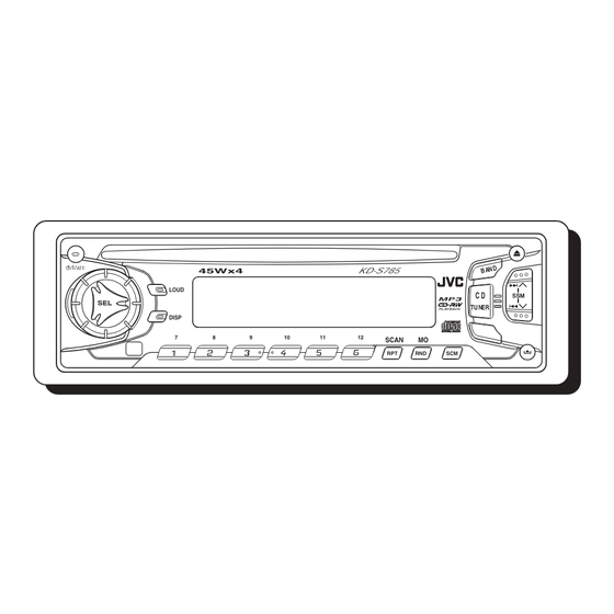
KD-S785
ATT
SOUND
U
LOUD
R
SOURCE
F
D
DISP
7
VOL
VOL
1-2
1-3
1-4
1-11
COPYRIGHT
2002 VICTOR COMPANY OF JAPAN, LTD.
45Wx4
KD-S785
TU NER
8
9
10
11
12
SCAN
MO
RPT
RND
SCM
U
operation untill TOC read
KD-S785
Area Suffix
Other Areas
1-12
1-14
1-14
1-15~33
No.49748
Jun. 2002
Advertisement
Table of Contents

Subscribe to Our Youtube Channel
Related Manuals for JVC KD-S785


Summary of Contents for JVC KD-S785
-
Page 1: Table Of Contents
KD-S785 SERVICE MANUAL CD RECEIVER KD-S785 SOUND 45Wx4 KD-S785 LOUD SOURCE TU NER DISP SCAN Area Suffix Other Areas Contents Safety precaution Flow of functional Preventing static electricity operation untill TOC read 1-12 Disassembly method Maintenance of laser pickup 1-14... -
Page 2: Safety Precaution
KD-S785 Safety precaution Burrs formed during molding may be left over on some parts of the chassis. Therefore, pay attention to such burrs in the case of preforming repair of this system. Please use enough caution not to see the beam directly or touch it in case of an... -
Page 3: Preventing Static Electricity
KD-S785 Preventing static electricity 1.Grounding to prevent damage by static electricity Electrostatic discharge (ESD), which occurs when static electricity stored in the body, fabric, etc. is discharged, can destroy the laser diode in the traverse unit (optical pickup). Take care to prevent this when performing repairs. -
Page 4: Disassembly Method
KD-S785 Disassembly method <Main body> Removing the front panel assembly (See Fig.1) Press the eject button in the lower right part of the front panel. Remove the front panel assembly from the body. Front panel assembly Eject button Fig.1 Tab a Removing the front chassis assembly (See Fig.2, 3) - Page 5 KD-S785 Removing the heat sink (See Fig.4) Remove the three screws A on the left side of the body. Heat sink Fig.4 Joint b Removing the bottom cover (See Fig.5, 6) Bottom cover Prior to performing the following procedure, remove the front panel assembly, the front chassis assembly and the heat sink.
- Page 6 KD-S785 Removing the main board (See Fig.7, 8) Prior to performing the following procedure, remove the front panel assembly, the front chassis assembly, the heat sink and the bottom cover. Remove the screw B, the four screws C and the three screws D attaching the rear bracket on the back of the body.
- Page 7 KD-S785 Removing the control switch board (See Fig.10 ~ 12) Prior to performing the following procedure, remove the front panel assembly. Remove the four screws G attaching the rear cover on the back of the front panel assembly. Rear cover Unjoint the eleven joints e with the front panel and the rear cover.
-
Page 8: Cd Mechanism Section
KD-S785 Damper bracket <CD mechanism section> CD mechanism assembly Removing the CD mechanism control board (See Fig.1 and 2) Unsolder the part a and b on the CD mechanism control board. Remove the stator fixing the CD mechanism control board and the damper bracket (To remove the stator smoothly, pick up the center part). - Page 9 KD-S785 Damper bracket assembly CD mechanism Removing the CD mechanism assembly (See Fig.1, 6 to 9) Prior to performing the following procedure, remove the CD mechanism control board and the front bracket (loading motor). Remove the three screws D and the damper bracket.
- Page 10 KD-S785 Removing the feed motor assembly FD screw Part i Feed motor assembly (See Fig.10) Prior to performing the following procedure, remove the CD mechanism control board, the front bracket Part j (loading motor) and the CD mechanism assembly. Remove the two screws F and the feed motor assembly.
-
Page 11: Adjustment Method
6. Digital tester FM 87.5MHz ~ 108.0MHz 7. Tracking offset meter AM 531kHz ~ 1602 kHz 8. Test Disc JVC :CTS-1000 9. Extension cable for check EXTGS004-26P 1 Dummy load Exclusive dummy load should be used for AM,and FM. For FM dummy load,there is a loss of 6dB between SSG output and antenna input.The loss of 6dB need not be considered... -
Page 12: Flow Of Functional
KD-S785 Flow of functional operation until TOC read Power ON • When the laser diode correctly Set Function to CD • When the pickup correctly moves emits to the inner area of the disc Microprocessor Microprocessor Disc inserted commands commands TC9462 "53"... - Page 13 KD-S785 Feed Section Check CD 9V Is the voltage output at Is the wiring for IC521 Is 5V present at IC581 and 5V. IC521 pin "53" 5V or 0V? (90) ~ (100) correct? pin "11"? Check the vicinity of IC521.
-
Page 14: Maintenance Of Laser Pickup
KD-S785 Maintenance of laser pickup (1) Cleaning the pick up lens Before you replace the pick up, please try to clean the lens with a alcohol soaked cotton swab. (2) Life of the laser diode When the life of the laser diode has expired, the following symptoms will appear. -
Page 15: Description Of Major Ics 1-15~33
KD-S785 Description of major ICs TC9490FA (IC541) : DSP & DAC 1.Pin layout & Block daiagram TEZI Clock generator SBAD 1-bit Servo control RFRP RFZI ZDET RFCT Digital equalizer Address automatic circuit adjustment circuit BUS0 Data CLV servo slicer BUS1... - Page 16 KD-S785 2.Pin function (1/2) TC9490FA(2/3) Pin No. Symbol Function Bit clock outputpin 32fs, 48fs, or 64fs selectable by command. LRCK L/R channel clock output pin."L" for L channe and "H" for R channel. Output polarity can be inverted by command.
- Page 17 KD-S785 2.Pin function (2/2) TC9490FA(3/3) Pin No. Symbol Function RFGC RF amplitude adjustment control signal output pin. TEBC Tracking balance control signal output pin. APC circuit ON/OFF signal output pin. At laser on,high impedance with UHS="L" ,H output with UHS="H".
- Page 18 KD-S785 UPD784215AGC172 (IC701) : Main micon 1.Pin layout 100 ~ 76 26 ~ 50 2.Pin functions(1/2) Symbol Pin No. Function CD mecha sw2 CD mecha sw3 CD mecha sw4 REST Rest sw Loading/Eject motor control (Loading side) Loading/Eject motor control (Eject side)
- Page 19 KD-S785 2.Pin functions(2/2) Pin No. Symbol Function SD/ST Station detector or stereo signal input LOCAL Loal or distance selecting output MONO Monoral selection output MP3 CLK CLK output for MP3 decoder MP3 DATA IN Data input for MP3 decoder / inverting input due to converter...
- Page 20 KD-S785 LA4743K (IC301) : Power amp. 1.Block diagram 2200 F 0.022 F Vcc 1/2 Vcc 3/4 IN 1 OUT 1+ 0.22 F OUT 1- PWR GND1 Protective circuit OUT 2+ IN 2 OUT 2- 0.22 F PWR GND2 ST BY...
- Page 21 KD-S785 2.Terminal layout 3.Pin function Pin No. Symbol Function Header of IC Power GND Outpur(-) for front Rch RFO- STBY Stand by input RFO+ Output (+) for front Rch Power input VCC1/2 RRO- Output (-) for rear Rch Power GND...
- Page 22 KD-S785 TA2147F-X (IC521) : RF amp. 1.Terminal layout 2.Block diagram PEAK GVSW 12 RFDC 20 A TEBC 50 A RFRP BOTTOM RFRPIN PEAK RFGO 1.75k 240k 15pF x0.5 RFGC 240k 15pF x0.5 AGCIN 180k 40pF 1-22...
- Page 23 KD-S785 3.Pin function Pin No. Symbol Function 3.3V Power supply pin Main-beam amp input pin Main-beam amp input pin Sub-beam amp input pin Sub-beam input pin Monitor photo diode amp input pin Laser diode amp output pin APC circuit ON/OFF control signal,laser diode (LDO) control signal input or bottom/peak detection frequency change pin.
- Page 24 KD-S785 TC94A02F-005 (IC401) : DSP AD10 VDDT LRCKiA BCKiA SDi0 AD13 VDDT AD14 /MiCK AD16 MiDio AD15 MiMD /RESET Timing Generator General Input Port 1-24...
- Page 25 KD-S785 3.Pin function(1/2) TC94A02F-005 Pin No. Symbol Function Hard reset input terminal(H:Normal operation L: Reset) /RESET Micon I/F mode select input terminal MiMD External SRAM address output 0 terminal External SRAM address output 1 terminal Micon I/F data input/output terminal...
- Page 26 KD-S785 3.Pin function(2/2) TC94A02F-005 Pin No. Symbol Function External SRAM data input/output 4 terminal Digital power supply (2.5V) terminal External SRAM data input/output 5 terminal External SRAM data input/output 6 terminal External SRAM data input/output 7 terminal VSSP VCO GND...
- Page 27 KD-S785 AN80T07 (IC901) : Regulator 1.Pin layout 2.Block diagram MODE1 *ASO,Peak Current Protection. *Thermal Protection (Except VDD,Comp output). Reference Voltage Outputs Driver Driver Driver Driver MODE2 SW5V Out COMP AUDIO BATT.DET 5.7V 8.0V 9.0V 3.Pin functions Pin No. Symbol Function SW5V Output When Mode 1 pin is "M","H"...
- Page 28 KD-S785 K6R1008VCTI12-X (IC451) : SRAM 1.Pin layout 2.Block diagram Clk Gen. Pre-Charge Circuit Memory Array 512 Rows 256x8 Columns SOJ/ Data I/O Circuit TSOP2 ~I/O Cont. Column Select Gen. 3.Pin function Pin Name Pin Function Address Inputs Write Enable Chip Select...
- Page 29 KD-S785 LA6574H-X (IC501) :CD driver 1.Terminal layout & brock daiagram Thermal Shutdown VCC2 1 28 REV POWER supplise 27 FWD V05- 2 26 S-GND V05+ 3 25 VCONT V04+ 4 V04- 5 24 VIN4 23 VIN4G V03+ 6 22 VCC-S...
- Page 30 KD-S785 LC75823W (IC601) : LCD driver 1. Pin Layout & Symbol 64 63 62 61 60 59 58 57 56 55 54 53 52 51 50 49 17 18 19 20 21 22 23 24 25 26 27 28 29 30 31 32 2.
- Page 31 KD-S785 NJM4565M-WE (IC581) : Ope. amp A OUTPUT A INPUT B OUTPUT B INPUT A INPUT B INPUT NJU7241F25-X (IC461) : Regulator 1.Pin layout 2.Block diagram Short protect GND 1 5 STB VIN 2 3 VOUT VIN 2 VOUT 3...
- Page 32 KD-S785 TB2118F-X (IC31) : PLL 1.Terminal Layout 2.Block diagram Constant power supply voltage Buff. ON/OFF AM CP. Phase OSC circuit Reference Counter Comparator switch FM VCO 4-bit Prescaler Swallow counter 12-bit AMVCO Programmable counter 20-bit BINARY COUNTER Resistor 1 22-bit...
- Page 33 KD-S785 TEA6320T-X (IC161) : E.volume 1.Pin layout 2.Block diagram VOLUME 2 MUTE 0 to 55 dB FUNCTION BALANCE OUTRR OUTLR ZERO CROSS FENDER REAR POWER DETECTOR OUTRF OUTLF SUPPLY VOLUME 1 BASS TREBLE +20 to -31 dB VOLUME 2 LEFT...
- Page 34 KD-S785 VICTOR COMPANY OF JAPAN, LIMITED MOBILE ELECTRONICS DIVISION PERSONAL & MOBILE NETWORK BUSINESS UNIT. 10-1,1Chome,Ohwatari-machi,Maebashi-city,371-8543,Japan 200206 (No.49748)
- Page 35 SERVICE MANUAL CD RECEIVER 49748B 2003 KD-S785 Area Suffix U ------------- Other Areas SOUND 45Wx4 LOUD SOURCE DISP SCAN TABLE OF CONTENTS PRECAUTION............... . . 1-3 SPECIFIC SERVICE INSTRUCTIONS .
- Page 36 SPECIFICATION AUDIO AMPLIFIER SECTION Maximum Power Output Front 45 W per channel Rear 45 W per channel 17 W per channel into 4 Ω, 40 Hz to 20 000 Hz at no more than Continuous Power Output Front (RMS) 0.8% total harmonic distortion. 17 W per channel into 4 Ω, 40 Hz to 20 000 Hz at no more than Rear 0.8% total harmonic distortion.
- Page 37 SECTION 1 PRECAUTION Please refer to "KD-S785 No.49748" about this section. SECTION 2 SPECIFIC SERVICE INSTRUCTIONS Please refer to "KD-S785 No.49748" about this section. SECTION 3 DISASSEMBLY Please refer to "KD-S785 No.49748" about this section. SECTION 4 ADJUSTMENT Please refer to "KD-S785 No.49748" about this section.
- Page 38 VICTOR COMPANY OF JAPAN, LIMITED AV & MULTIMEDIA COMPANY MOBILE ENTERTAINMENT CATEGORY 10-1,1chome,Ohwatari-machi,Maebashi-city,371-8543,Japan (No.49748B) Printed in Japan...
- Page 39 PARTS LIST [ KD-S785 ] * All printed circuit boards and its assemblies are not available as service parts. Area suffix U --------------------- Other Areas - Contents - 3- 2 Exploded view of general assembly and parts list (Block No.M1) 3- 4 CD mechanism assembly and parts list (Block No.MB)
- Page 40 Exploded view of general assmbly and parts list Block No.
- Page 41 General assembly Block No. [M][1][M][M] Symbol No. Part No. Part Name Description Local QYSDST2004Z SCREW 2mm x 4mm LV40847-002A SPACER FSJC1029-401 TOP CHASSIS FSMH3001-202 SIDE PANEL FSKM3011-002 BOTTOM COVER FSMA3004-203 INSULATOR QYSDST2604Z SCREW 2.6mm x 4mm(x3) FSKZ4005-001 SCREW (x2) QYSDST2604Z SCREW 2.6mm x 4mm(x3)
- Page 42 CD mechanism assembly and parts list Block No. Grease G-31SA TN-CCD1001Z-138S G-31SA(Bottom side) RX-405 106 29...
- Page 43 CD mechanism Symbol No. Part No. Part Name Description Local Block No. [M][B][M][M] 303105310T FEED MO ASSY Symbol No. Part No. Part Name Description Local 303105311T SPINDLE MO ASSY 303105312T FEED SCREW ASSY 303111301T LDG MOTOR ASSY 30310101T FRAME 303111302T RDG RLR SFT ASY...
- Page 44 Electrical parts list Main board Symbol No. Part No. Part Name Description Local Block No. [0][1][0][0] D972 CRS03-W SB DIODE Symbol No. Part No. Part Name Description Local D981 1SS355-X SI DIODE D982 1SS355-X SI DIODE IC31 TB2118F-X PLL IC QEKJ1CM-226Z E CAPACITOR...
- Page 45 Symbol No. Symbol No. Part No. Part Name Description Local Part No. Part Name Description Local C318 QEKJ1CM-226Z E CAPACITOR 22uF 16V M C560 NCB31HK-103X C CAPACITOR 0.01uF 50V K C319 NCB31EK-223X C CAPACITOR 0.022uF 25V K C561 QERF1AM-107Z E CAPACITOR 100uF 10V M...
- Page 46 Symbol No. Symbol No. Part No. Part Name Description Local Part No. Part Name Description Local NRS181J-100X MG RESISTOR 10Ω 1/8W J R521 NRSA63J-823X MG RESISTOR 82kΩ 1/16W J NRSA63J-622X MG RESISTOR 6.2kΩ 1/16W J R522 NRSA63J-823X MG RESISTOR 82kΩ...
-
Page 47: Front Board
Symbol No. Front board Part No. Part Name Description Local Block No. [0][2][0][0] R726 NRSA63J-103X MG RESISTOR 10kΩ 1/16W J Symbol No. R728 NRSA63J-103X MG RESISTOR 10kΩ 1/16W J Part No. Part Name Description Local R729 NRSA63J-473X MG RESISTOR 47kΩ... - Page 48 Symbol No. Part No. Part Name Description Local R649 NRSA63J-122X MG RESISTOR 1.2kΩ 1/16W J R651 NRSA63J-222X MG RESISTOR 2.2kΩ 1/16W J R652 NRSA63J-222X MG RESISTOR 2.2kΩ 1/16W J R653 NRSA63J-103X MG RESISTOR 10kΩ 1/16W J R654 NRSA63J-103X MG RESISTOR 10kΩ...
- Page 49 <MEMO> 3-11...
- Page 50 Packing materials and accessories parts list Block No. A1,A2,A3 KIT : A4.A5,A6 A7,A8 3-12...
- Page 51 Packing and accessories Block No. [M][3][M][M] Symbol No. Part No. Part Name Description Local GET0060-001A INST BOOK ENG CHI THA ARA GET0060-002A INSTALL MANUAL LVT0918-001A MP3 SHEET VKZ4027-202 PLUG NUT VKH4871-001SS MOUNT BOLT VKZ4328-001 LOCK NUT WNS5000Z WASHER FSKL4010-002 HOOK (x2) FSJB3001-30C...
- Page 52 SCHEMATIC DIAGRAMS CD RECEIVER KD-S785 CD-ROM No.SML200312 Area Suffix U ------------- Other Areas SOUND 45Wx4 LOUD SOURCE DISP SCAN Contents Safety precaution ------------------------ 2-2 Block diagram ----------------------------- 2-3 Standard schematic diagrams -------- 2-4 Printed circuit boards -------------------- 2-7 No.49748BSCH COPYRIGHT 2003 VICTOR COMPANY OF JAPAN, LIMITED.
- Page 53 Safety precaution Burrs formed during molding may be left over on some parts of the chassis. Therefore, pay attention to such burrs in the case of preforming repair of this system. Please use enough caution not to see the beam directly or touch it in case of an adjustment or operation check.
- Page 54 Block diagram OUTLF,OUTLR TUL,TUR IC161 OUTRF,OUTRR TUNER E.VOL LOADING+ PACK LOADING- LOADING LOADING+ SPINDLE+ AMVT IC501 LOADING- MOTOR SPINDLE- FMVT FEED+,FEED- DRIVER FOCUS+,FOCUS- IC31 DMO,FMO SEEK/STOP IC301 TRACKING+ REST SM,FM/AM REST FOO,TRD POWER TRACKING- MONO SWITCH LOCAL IC521 VA,VB,VC,VD,VE,VF SD/ST MD,LD RF AMP LEVEL...
- Page 55 Standard schematic diagrams Main amplifier section D243 1SS133 R244 C243 R243 0.047 180k R245 C241 R247 1/50 R242 R241 IC301 C242 22/16 LA4743K Q241 QAU0258-002 2SD601A( R) LEVEL R161 D240 2.2/50 4.7u 220k 1SS355-X C312 R312 OUTLF OUTLR 1/50 1/50 1.2k R311 220k...
- Page 56 CD Servo control section R502 6.8k R503 5.6k R586 R584 C582 R587 CD.R R501 6.8k R-CH R581 R585 C584 1.5k 4.7/25 C503 R506 47/6.3 8.2k C587 Q501 C581 150p CN601 2SB1322 560p D501 QGB2027M2-26S DSK10C-T1 C591 C597 150p 560p C592 R597 L-CH R591...
- Page 57 LCD & Key control section QSW0863-001 JS690 RPM6938-SV4 IC602 0.022 R661 C681 R662 VCM0335-001 CJ601 LCD1 ACC5V QLD0225-001 REMOCON ENC1 ENC2 BUS2 LCDCL LCDDA LCDCE KEY0 BUS1 KEY1 KEY2 IC601 R605 R604 R603 R602 R601 Key0 LC75823W 3.9k 2.7k 1.8k 1.2k 1.8k 2.2k...
- Page 58 Printed circuit boards Main board (Forward side) R904 IC901 C914 C901 C904 L901 D341 C802 C911 J801 J321 Q321 CN901 C913 C905 Q341 D902 C902 C163 D901 Q891 R901 R341 C173 C910 C907 R321 R331 R351 C316 C903 C244 C241 Q881 C318 R852...
- Page 59 Main board (Reverse side) C916 C917 C891 IC901 R971 J321 C912 R972 D972 L901 C325 D971 J801 C906 D901 C324 C323 C904 CN901 C914 C322 R902 C852 C971 C163 C173 Q351 Q331 C905 C913 R901 C241 C244 C907 C910 R903 C903 C318 C902...
- Page 60 < MEMO > 2-5 (No.49748BSCH)
- Page 61 VICTOR COMPANY OF JAPAN, LIMITED MOBILE ELECTRONICS DIVISION PERSONAL & MOBILE NETWORK BUSINESS UNIT. 10-1,1Chome,Ohwatari-machi,Maebashi-city,371-8543,Japan No.49748BSCH...
- Page 62 KD-S785 PARTS LIST [ KD-S785 ] * All printed circuit boards and its assemblies are not available as service parts. Area suffix U --------------------- Other Areas - Contents - 3- 2 Exploded view of general assembly and parts list (Block No.M1) 3- 5 CD mechanism assembly and parts list (Block No.MB)
- Page 63 KD-S785 Exploded view of general assembly and parts list Block No.
- Page 64 KD-S785 Parts list (General assembly) Block No. M1MM Item Description Parts number Parts name Q'ty Area ------------ CD MECHA (1325) FSJC1029-401 TOP CHASSIS FSMH3001-202 SIDE PANEL FSKM3011-002 BOTTOM COVER FSMA3004-203 INSULATOR QYSDST2604Z SCREW 3 CHASSIS+MECHA BKT FSKZ4005-001 SCREW 2 CHASSIS+SIDE PANEL...
- Page 65 KD-S785 Parts list (General assembly) Block No. M1MM Item Parts number Parts name Q'ty Description Area QYSDST2606Z SCREW 1 FOR ANT QYSDSF3006Z SCREW 1 FOR LINE OUT QYSDST2606Z SCREW 3 16P & REG BKT QYSDST2004Z SCREW LV40847-002A SPACER FSYH4036-069 SHEET...
- Page 66 KD-S785 CD mechanism assembly and parts list Block No. Grease G-31SA TN-CCD1001Z-138S G-31SA(Bottom side) RX-405 106 29...
- Page 67 KD-S785 Parts list (CD mechanism) Block No. MBMM Item Description Parts number Parts name Q'ty Area 30310101T FRAME 30310103T DANPER PIN 30310107T UPPER PLATE 30310108T SEL STOP PLATE 30310142T SEL ARM (L)L 30310143T SEL ARM (R)L 30310145T S ARM SPRING(L)
- Page 68 KD-S785 Parts list (CD mechanism) Block No. MBMM Item Description Parts number Parts name Q'ty Area 68150242T CONNECTOR 1 TKC-W26X-A1 30311105T SOPPORT PLATE GR MT BLK(N) 30311138T 30311109T LDG GEAR (2) 30311110T LDG GEAR (3) 30311112T LDG GEAR (5) 30311136T...
- Page 69 KD-S785 Electrical parts list (Main board) Block No. 01 Item Parts number Parts name Remarks Area Item Parts number Parts name Remarks Area QEKJ1CM-226Z E CAPACITOR 22MF 20% 16V C 303 NCS31HJ-391X C CAPACITOR NCB31EK-473X C CAPACITOR C 304 NCS31HJ-391X...
- Page 70 KD-S785 Electrical parts list (Main board) Block No. 01 Item Parts number Parts name Remarks Area Item Parts number Parts name Remarks Area C 526 QERF1AM-107Z E CAPACITOR 100MF 20% 10V C 781 QERF0JM-476Z E CAPACITOR 47MF 20% 6.3V C 527...
- Page 71 KD-S785 Electrical parts list (Main board) Block No. 01 Item Parts number Parts name Remarks Area Item Parts number Parts name Remarks Area D 852 CRS03-W SB DIODE NRSA63J-472X MG RESISTOR D 901 1N5401-TU-15 DIODE NRSA63J-470X MG RESISTOR D 902...
- Page 72 KD-S785 Electrical parts list (Main board) Block No. 01 Item Parts number Parts name Remarks Area Item Parts number Parts name Remarks Area R 411 NRSA63J-225X MG RESISTOR R 583 NRSA63J-223X MG RESISTOR R 412 NRSA63J-0R0X MG RESISTOR R 584...
- Page 73 KD-S785 Electrical parts list (Main board) Block No. 01 Item Remarks Parts number Parts name Area R 783 NRSA63J-102X MG RESISTOR R 784 NRSA63J-473X MG RESISTOR R 851 NRSA63J-103X MG RESISTOR R 901 QRE142J-102X C RESISTOR 1.0K 5% 1/4W R 902...
- Page 74 KD-S785 Electrical parts list (Front board) Block No. 02 Item Parts number Parts name Remarks Area Item Parts number Parts name Remarks Area C 601 NCB31HK-223X C CAPACITOR R 639 NRSA63J-511X MG RESISTOR C 602 NCS31HJ-681X C CAPACITOR R 640...
- Page 75 KD-S785 Packing materials and accessories parts list Block No. Block No. A1~A3 A13, A14 KIT : A4~A8 3-14...
- Page 76 KD-S785 Parts list (Packing) Block No. M3MM Item Description Parts number Parts name Q'ty Area FSPG4002-001 POLY BAG 1 FOR INST BOOK QPA00801205 POLY BAG 1 FOR SCREW KIT POLY BAG 1 FOR HARD CASE QPA01003003 FSYH4036-068 SHEET QPC03004315P POLY BAG...
-
Page 77: Schematic Diagrams
KD-S785 SCHEMATIC DIAGRAMS CD RECEIVER KD-S785 CD-ROM No.SML200201 SOUND 45Wx4 LOUD SOURCE DISP SCAN Area Suffix Other Areas Contents Block diagram Standard schematic diagrams Printed circuit boards 2-5,6 No.49748 COPYRIGHT 2002 VICTOR COMPANY OF JAPAN, LTD. Jun. 2002... - Page 78 Safety precaution Burrs formed during molding may be left over on some parts of the chassis. Therefore, pay attention to such burrs in the case of preforming repair of this system. Please use enough caution not to see the beam directly or touch it in case of an adjustment or operation check.
- Page 79 KD-S785 Block diagram OUTLF,OUTLR TUL,TUR IC161 OUTRF,OUTRR TUNER E.VOL LOADING+ PACK LOADING- LOADING LOADING+ SPINDLE+ AMVT IC501 MOTOR LOADING- SPINDLE- FMVT FEED+,FEED- DRIVER FOCUS+,FOCUS- IC31 SEEK/STOP DMO,FMO IC301 TRACKING+ REST FOO,TRD SM,FM/AM REST POWER TRACKING- MONO SWITCH LOCAL IC521 VA,VB,VC,VD,VE,VF...
- Page 80 KD-S785 KD-S785 Standard schematic diagrams D243 1SS133 R244 C243 Main amp section R243 0.047 180k R245 C241 R247 1/50 R242 R241 IC301 C242 22/16 LA4743K Q241 QAU0258-001 2SD601A( R) LEVEL R171 D241 2.2/50 4.7u 220k 1SS355-X C312 R312 OUTLF OUTLR...
- Page 81 KD-S785 CD servo control section R502 6.8k R503 5.6k R586 R584 1SS355-X R587 C582 R581 CD.R R501 6.8k D981 R-CH R585 2SB709A/R/-X C584 1.5k Q982 8.2k 4.7/25 C503 Q981 R981 R506 47/6.3 UN2211 8.2k C587 Q501 D982 C581 150p CN601...
- Page 82 KD-S785 KD-S785 LCD & Key control section QSW0863-001 JS690 RPM6938-SV4 IC602 0.022 R661 C681 R662 VCM0335-001 CJ601 LCD1 ACC5V QLD0225-001 REMOCON ENC1 ENC2 BUS2 LCDCL LCDDA LCDCE KEY0 BUS1 KEY1 KEY2 IC601 R605 R604 R603 R602 R601 Key0 LC75823W 3.9k 2.7k...
- Page 83 KD-S785 Printed circuit boards Main board(Foward side) R904 IC901 C914 C901 C904 L901 D341 C802 C911 J801 J321 Q321 CN901 C913 C905 Q341 D902 C902 C163 D901 Q891 R901 R341 C173 C910 C907 R321 R351 R331 C316 C903 C244 C241...
- Page 84 KD-S785 Main board(Reverse side) C916 C917 C891 IC901 CONT R971 J321 C912 R972 D972 L901 C325 D971 J801 C906 C324 C323 D901 C904 CN901 C914 C322 R902 C852 C971 C163 C173 Q351 Q331 C905 C913 R901 C241 C244 C907 C910...
- Page 85 < M E M O >...
- Page 86 KD-S785 VICTOR COMPANY OF JAPAN, LIMITED MOBILE ELECTRONICS DIVISION PERSONAL & MOBILE NETWORK BUSINESS UNIT. 10-1,1Chome,Ohwatari-machi,Maebashi-city,371-8543,Japan 200206 (No.49748)
Need help?
Do you have a question about the KD-S785 and is the answer not in the manual?
Questions and answers