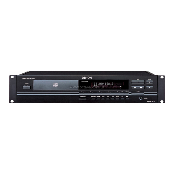
Denon DN-C615 Service Manual
Stereo cd/mp3
Hide thumbs
Also See for DN-C615:
- Operating instructions manual (76 pages) ,
- Service manual (2 pages) ,
- Operating instructions manual (16 pages)
Advertisement
Table of Contents
- 1 Specifications
- 2 Top Cover
- 3 Front Panel
- 4 Mechanism Unit
- 5 Service Program
- 6 Block Diagram
- 7 Top View
- 8 Note for Parts List
- 9 Parts List of P.w.b. Unit Ass'y
- 10 Parts List of Exploded View
- 11 Wiring Diagram
- 12 Level Diagram
- 13 Packing View
- 14 Parts List of Packing & Accessories
- Download this manual
Advertisement
Table of Contents

Related Manuals for Denon DN-C615


Summary of Contents for Denon DN-C615
- Page 1 For U.S.A., Canada, Europe, Korea model SERVICE MANUAL DN-C615 MODEL STEREO CD/MP3 PLAYER Some illustrations using in this service manual are slightly different from the actual set. 16-11, YUSHIMA 3-CHOME, BUNKYOU-KU, TOKYO 113-0034 JAPAN Telephone: 03 (3837) 5321 X0160 NC 0211...
-
Page 2: Specifications
DN-C615 SAFETY PRECAUTIONS The following check should be performed for the continued protection of the customer and service technician. LEAKAGE CURRENT CHECK Before returning the unit to the customer, make sure you make either (1) a leakage current check or (2) a line to chassis resistance check. -
Page 3: Top Cover
DN-C615 DISASSEMBLY (To reassemble, reverse disassembly) 1. TOP COVER Remove 4screws from both sides and 2 screws from back Panel. Screw Top cover Screw Screw 2. FRONT PANEL Pull Loader frame frontward, and remove loader panel. Remove 2 front panel upper screws. -
Page 4: Mechanism Unit
DN-C615 3. MECHANISM UNIT 3.1. How to remove a mechanism unit in case a power supply is not turned on. Remove 4 screws on the Mecha base. Remove the CD Mecha to the arrow direction. Detach the Loader panel to the arrow direction. - Page 5 DN-C615 3.2. How to remove a mechanism unit in case a power supply is turned on. Remove 4 screws. Screw Screw...
-
Page 6: Service Program
DN-C615 SERVICE PROGRAM 1. REQUIRED MEASURING IMPLEMENT • Reference disc (TCD784 or CO-74176) 1.1. What is Service Program Service program is a special program intended for confirming servo functions etc. 1.2. µcom Version Check • Refer to "Preset Functions and Operations" of the instruction manual. - Page 7 DN-C615 1.4. Test Mode (Heat Run mode) • Switch on the power while pushing the 3 button and 4 button at the same time. "000TroHR0000" is displayed. And the tray is opened Hold the disc by the edges and place it on the disc tray.
- Page 8 DN-C615 Error Code CONTENTS Error 19 The focus fine gain is outside the regulation range. Error 1A Unable to adjust the tracking fine gain in the regulation time. Error 1B The tracking fine gain is outside the regulation range. Error 1C Unable to adjust automatically in the regulation time.
-
Page 9: Block Diagram
DN-C615 BLOCK DIAGRAM <CD MUTE> 16M DRAM DIGITAL MUTE P. TRANS CD MECHA MOTOR DRIVER 3.3V 5V ACTUATOR MUTE CD OUT AN8785SB TC74HCT7007 PCM1716E HEAD AMP MN662791 H/P OUT AN22002A MUTE 5V 3.3V SN74LV244 CLOCK GEN 3.3V 5V TC74HCT7007 SYSTEM uCOM... - Page 10 DN-C615 SEMICONDUCTORS IC’s MN102H60KDA (IC101) MN102H60KDA Terminal Function Pin Name Symbol Function P60, WAIT, SBT2 PCDMUTE Mute for CD P61, _RE Hi-Z Read signal P62, _WEL _WEL Hi-Z Write signal P63, _WE, _WEH PEXTIN Hi-Z EXT.IN signal _CS0,TM13OA _CS0 Hi-Z...
- Page 11 DN-C615 Pin Name Symbol Function P33,A11,_KI3 Unfix Address bus AVDD AVDD Analog power supply terminal P34,A12,_KI4 Unfix Address bus P35,A13,_KI5 Unfix Address bus P36,A14,_KI6 Unfix Address bus P37,A15,_KI7 Unfix Address bus P40,A16 Unfix Address bus P41,A17 Unfix Address bus P42,A18...
- Page 12 DN-C615 Pin Name Symbol Function _RST _RESET Reset signal 'L': RESET Power supply (+3.3V) P00,D00,AD00 Hi-Z Data bus P01,D01,AD01 Hi-Z Data bus P02,D02,AD02 Hi-Z Data bus P03,D03,AD03 Hi-Z Data bus P04,D04,AD04 Hi-Z Data bus P05,D05,AD05 Hi-Z Data bus P06,D06,AD06 Hi-Z...
- Page 13 DN-C615 MN6627911AC (IC201) MN6627911AC Terminal Function Pin No. Pin Name Function DRVDD Power supply for DRAM interface (Pin No.2 - 18, 80) Data I/O signal 0 for DRAM Data I/O signal 1 for DRAM Write enable signal for DRAM RAS control signal for DRAM...
- Page 14 DN-C615 Pin No. Pin Name Function DSLF Loop filter for DSL RFSW Loop filter for DSL PLLF Loop filter for PLL PLLFO Loop filter for PLL AVDD2 Power supply for analog (DSL, PLL, AD) AVSS2 GND for analog (DSL, PLL, AD)
- Page 15 DN-C615 AN8785SB (IC202) L: All mute [ Others ] Hiz: ch2,4 ON [ Loading ] [ Traverse ] [ Spindle ] [ Focus ] [ Tracking ] H: Active Standby PVcc2 PVcc3 PVcc1 Protection Circuit Standby Band-gap Vcc/Vref Reser Circuit 1.25V...
- Page 16 DN-C615 PCM 1716E (IC206) NAME DESCRIPTION LRCIN Left and Right Clock Input. This clock is equal to the sampling rate - f LRCIN ML/IIS Serial Audio Data Input BCKIN Bit Clock Input for Serial Audio Data. MC/DM1 CLKO Buffered Output of Oscillator. Equivalent to...
- Page 17 DN-C615 M66005FP (IC701) D I G D I G D I G D I G D I G D I G D i s p l a y C o d e R e g i s t e r...
- Page 18 DN-C615 16M DRAM (IC204) 4M FLASH MEMORY (IC111) SN74LV02APW (IC107) I/O1 I/O4 4 3 2 1 32 31 30 I/O2 I/O3 14 15 16 17 18 19 20 TC7WU04F BA15218F (IC102,207) NJM78M05FA(S) (IC118,902) BA033T (IC901) A OUTPUT A –INPUT B OUTPUT...
- Page 19 DN-C615 TC74HCT7007AF (IC109, 112) SN74LV541APW (IC104) TC9246F (IC114) Lock Ditection Microcomputer Interface Circuit Programmable Counter Phase Selector Comparator SN74LV573APW (IC103) SN74LV244APW (IC116) AN80L18RMS (IC205)
-
Page 20: Top View
DN-C615 1 TRANSISTORS DTA114EK DTC114EK DTA Series DTC Series 2SB709A VIEW KTC2875B DTA144ES FRONT VIEW 10ko hm 10ko hm 10ko hm 10ko hm DTC114EK DTA114EK DTA144ES 47ko hm 47ko hm 2SB562(C) 2SD2144 FRONT VIEW 1 DIODES/LED S4VB20 1SS355 1SR35-400A TOP VIEW... - Page 21 DN-C615 FL DISPLAY BJ896GN(FL701) 2-1 3-1 4-1 5-1 Pin connection Pin No. Connection Pin No. Connection Anode connection NOTE 1) F1,F2 : Filament 2) NP : No pin 1G~10G 3) NC : No connection 4) DL : Datum Line 5) 1G~14G : Grid...
- Page 22 DN-C615 PRINTED WIRING BOARD GU-3502 MAIN UNIT Ass'y Parts List COMPONENT SIDE...
- Page 23 DN-C615 GU-3502 MAIN UNIT Ass'y Parts List FOIL SIDE...
-
Page 24: Note For Parts List
DN-C615 NOTE FOR PARTS LIST Part indicated with the mark " " are not always in stock and possibly to take a long period of time for supplying, or in some case supplying of part may be refused. When ordering of part, clearly indicate "1" and "I" (i) to avoid mis-supplying. -
Page 25: Parts List Of P.w.b. Unit Ass'y
DN-C615 PARTS LIST OF P.W.B. UNIT ASS'Y Ref. No. Part No. Part Name Remarks Q’ty SEMICONDUCTORS GROUP IC101 262 3171 000 MN102H60KDA IC102 263 0615 902 BA15218F-DXE2 IC103 262 2642 909 SN74LV573APW-EL2 IC104 262 2641 900 SN74LV541APW-EL2 IC107 262 2729 903... - Page 26 DN-C615 Ref. No. Part No. Part Name Remarks Q’ty ZD901 276 0643 983 MTZJ5.1A T77 ZD902 276 0762 929 MTZJ30B T77 RESISTORS GROUP R101,102 247 2011 942 RM73B--473JT R104 247 2011 942 RM73B--473JT R105 247 2005 987 RM73B--221JT R107,108 247 2011 942...
- Page 27 DN-C615 Ref. No. Part No. Part Name Remarks Q’ty R214 247 2010 985 RM73B--273JT R215 247 2011 900 RM73B--333JT R216 247 2010 927 RM73B--153JT R217 247 2010 969 RM73B--223JT R218 247 2011 926 RM73B--393JT R219 247 2010 927 RM73B--153JT R220,221...
- Page 28 DN-C615 Ref. No. Part No. Part Name Remarks Q’ty R346 247 2011 942 RM73B--473JT R348 247 2009 983 RM73B--103JT R352 247 2011 942 RM73B--473JT R358 247 2013 940 RM73B--334JT R361,362 247 2018 903 RM73B--0R0KT R363 247 2009 925 RM73B--562JT R501...
- Page 29 DN-C615 Ref. No. Part No. Part Name Remarks Q’ty C158 257 0512 903 CK73F1E104ZT C160 257 0511 904 CK73F1H103ZT C161 257 0512 903 CK73F1E104ZT C165 254 4536 915 CE04W1A470MT SMG/RE3 C166 257 0512 903 CK73F1E104ZT C169,170 257 0512 903 CK73F1E104ZT...
- Page 30 DN-C615 Ref. No. Part No. Part Name Remarks Q’ty C270 257 0501 901 CK73B1H103KT (1608) C271 257 0512 903 CK73F1E104ZT C272 254 4538 926 CE04W1C330MT SMG/RE3 C273 257 0501 901 CK73B1H103KT (1608) C274 257 0512 903 CK73F1E104ZT C275 254 4538 900...
- Page 31 DN-C615 Ref. No. Part No. Part Name Remarks Q’ty CX231 205 1100 009 23P FFC BASE(P=1) CY22 205 0453 016 2P VH CONN BASE(L) CY231 205 1100 009 23P FFC BASE(P=1) F981 206 1087 057 FUSE (ET0.4A) FB101-105 235 0130 903...
- Page 32 DN-C615 EXPLODED VIEW OF CABINETW WARNING: Parts marked with this symbol have critical Parts List characteristics. Use ONLY replacement parts recommended by the manufacturer. 1 -1 50 33 1 -2 1 -3...
-
Page 33: Parts List Of Exploded View
DN-C615 PARTS LIST OF EXPLODED VIEW Note: The symbols in the column “Remarks” indicate the following destinations. E3:U.S.A. & Canada model E2: Europe model E2K:Korea model Ref. No. Part No. Part Name Remarks Q'ty GU-3502 MAIN UNIT MAIN UNIT DISPLAY SW UNIT... - Page 34 DN-C615 Ref. No. Part No. Part Name Remarks Q'ty GEN 6131-2 R. SHEET E2 SUB ASS’Y For E2 GEN 6212 R. SHEET(K) SUB ASS’Y For E2K SCREWS 473 7015 018 3X8 CBTS (S)-B 473 7004 003 4X8 CBTS (S)-Z 473 8007 025...
- Page 35 DN-C615 EXPLODED VIEW OF CD MECHANISM UNIT (CD11FTA3N) PARTS LIST OF CD MECHANISM UNIT Ref. No. Part No. Part Name Remarks Q'ty Ref. No. Part No. Part Name Remarks Q'ty 1 964 0009 006 Frame chassis 11 964 0010 008 Mecha lifter...
-
Page 36: Wiring Diagram
DN-C615 WIRING DIAGRAM... -
Page 37: Level Diagram
DN-C615 LEVEL DIAGRAM IC207 LINE OUT 1(7) IC602 LOAD 33 ohm 1(7) HEADPHONE (dBV) +10dB +8dB (RCA) +3.0dB -5.6dB +6dB +2dB -12dB -6.6dB (HEADPHONE) -10dB... -
Page 38: Packing View
DN-C615 PACKING VIEW PARTS LIST OF PACKING & ACCESSORIES Note: The symbols in the column “Remarks” indicate the following destinations. E3:U.S.A. & Canada model E2: Europe model E2K:Korea model Ref. No. Part No. Part Name Remarks Q'ty 505 0102 092... - Page 39 DN-C615 SCHEMATIC DIAGRAMS (1/2) WARNING: NOTICE Parts marked with this symbol have critical characteristics. ALL RESISTANCE VALUES IN OHM. k=1,000 OHM M=1,000,000 OHM Use ONLY replacement parts recommended by the manufacture. ALL CAPACITANCE VALUES IN MICRO FARAD. P=MICRO-MICRO FARAD EACH VOLTAGE AND CURRENT ARE MEASUERD AT MO SIGNAL INPUT CAUTION: CONDITION.
- Page 40 DN-C615 SCHEMATIC DIAGRAMS (2/2) ± B LINE WARNING: Parts marked with this symbol have critical characteristics. SIGNAL LINE Use ONLY replacement parts recommended by the manufacture. CAUTION: Before returning the unit to the customer, make sure you make either (1) a leakage current check or (2) a line to chassis resistance check.
Need help?
Do you have a question about the DN-C615 and is the answer not in the manual?
Questions and answers