Table of Contents
Advertisement
Quick Links
CDX-GT700D/GT705DX
SERVICE MANUAL
Ver. 1.0 2005.12
• The tuner and CD sections have no adjustments.
AUDIO POWER SPECIFICATIONS (US MODEL)
POWER OUTPUT AND TOTAL HARMONIC DISTORTION
23.2 watts per channel minimum continuous average power into
4 ohms, 4 channels driven from 20 Hz to 20 kHz with no more
than 5% total harmonic distortion.
CD player section
Signal-to-noise ratio
120 dB
Frequency response
10 – 20,000 Hz
Wow and flutter
Below measurable limit
Tuner section
FM
Tuning range
CDX-GT705DX: 87.5 – 107.9 MHz
CDX-GT700D: 87.5 – 108 MHz
Antenna terminal
External antenna connector
Intermediate frequency
10.7 MHz/450 kHz
Usable sensitivity
9 dBf
Selectivity
75 dB at 400 kHz
Signal-to-noise ratio
67 dB (stereo), 69 dB (mono)
Harmonic distortion at 1 kHz
0.5% (stereo), 0.3% (mono)
Separation
35 dB at 1 kHz
Frequency response
30 – 15,000 Hz
AM (CDX-GT705DX)
Tuning range
530 – 1,710 kHz
Antenna terminal
External antenna connector
Intermediate frequency
10.7 MHz/450 kHz
Sensitivity
30 µV
MW/LW (CDX-GT700D)
Tuning range
MW: 531 – 1,602 kHz
LW: 153 – 279 kHz
Antenna terminal
External antenna connector
Intermediate frequency
10.7 MHz/450 kHz
Sensitivity
MW: 30 µV
LW: 40 µV
Sony Corporation
9-887-002-01
eVehicle Division
2005L04-1
Published by Sony Engineering Corporation
© 2005.12
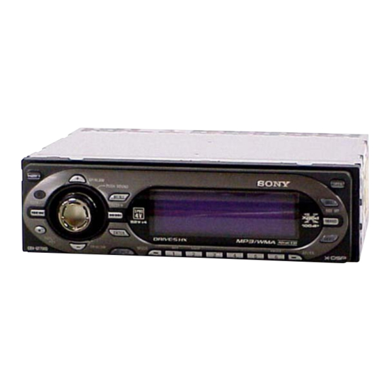
Photo: CDX-GT700D
Model Name Using Similar Mechanism
CD Drive Mechanism Type
Optical Pick-up Name
SPECIFICATIONS
Power amplifier section
Outputs
Speaker impedance
Maximum power output 52 W × 4 (at 4 ohms)
General
Outputs
Inputs
Loudness
FM/AM COMPACT DISC PLAYER
FM/MW/LW COMPACT DISC PLAYER
US Model
Canadian Model
CDX-GT705DX
AEP Model
UK Model
E Model
CDX-GT700D
CDX-GT800D/GT805DX
MG-611WD-186//Q
KSS1000E
Speaker outputs (sure seal connectors)
4 – 8 ohms
Audio outputs terminal (front/rear)
Subwoofer output terminal (mono)
Power antenna relay control terminal
Power amplifier control terminal
Telephone ATT control terminal
Illumination control terminal
BUS control input terminal
BUS audio input/AUX IN terminal
Remote controller input terminal
Antenna input terminal
+8 dB at 100 Hz
+0 dB at 10 kHz
– Continued on next page –
CDX-GT705DX
CDX-GT700D
Advertisement
Table of Contents

Related Manuals for Sony CDX-GT700D


Summary of Contents for Sony CDX-GT700D
- Page 1 General Outputs Audio outputs terminal (front/rear) Tuning range CDX-GT705DX: 87.5 – 107.9 MHz Subwoofer output terminal (mono) CDX-GT700D: 87.5 – 108 MHz Power antenna relay control terminal Antenna terminal External antenna connector Power amplifier control terminal Intermediate frequency 10.7 MHz/450 kHz...
- Page 2 THE PARTS LIST ARE CRITICAL TO SAFE OPERATION. CRITIQUES POUR LA SÉCURITÉ DE FONCTIONNEMENT. NE REPLACE THESE COMPONENTS WITH SONY PARTS REMPLACER CES COMPOSANTS QUE PAR DES PIÈCES SONY WHOSE PART NUMBERS APPEAR AS SHOWN IN THIS DONT LES NUMÉROS SONT DONNÉS DANS CE MANUEL OU MANUAL OR IN SUPPLEMENTS PUBLISHED BY SONY.
- Page 3 CDX-GT700D/GT705DX • CD Playback: You can play CD-DA (also containing CD TEXT* ), CD-R/CD- RW (MP3/WMA files also containing Multi Session and ATRAC CD (ATRAC3 and ATRAC3plus format). Type of discs Label on the disc CD-DA ATRAC CD *1 A CD TEXT disc is a CD-DA that includes information such as disc, artist and track name.
-
Page 4: Table Of Contents
CDX-GT700D/GT705DX • UNLEADED SOLDER TABLE OF CONTENTS Boards requiring use of unleaded solder are printed with the lead- free mark (LF) indicating the solder contains no lead. GENERAL (Caution: Some printed circuit boards may not come printed with Location of Controls ............5 the lead free mark due to their particular size.) -
Page 5: General
CDX-GT700D/GT705DX SECTION 1 This section is extracted GENERAL from instruction manual. • LOCATION OF CONTROLS • CDX-GT700D (AEP, UK Model) Location of controls and basic operations Main unit E GP* T Disc slot 5 /ALBM* +/– buttons* To select preset stations/skip groups (press);... - Page 6 CDX-GT700D/GT705DX • CDX-GT700D (AEP, UK Model) Auxiliary equipment such as portable Note for the aerial connecting Hinweis zum Anschließen der Antenne Remarque sur le raccordement de Nota per il collegamento dell’antenna Opmerking bij de antenne-aansluiting If your car aerial is an ISO (International Wenn Ihre Fahrzeugantenne der l’antenne...
- Page 7 CDX-GT700D/GT705DX • LOCATION OF CONTROLS • CDX-GT700D (E Model) Location of controls and basic operations Main unit E GP* R RESET button 4 /ALBM* +/– buttons* To select preset stations/skip groups (press); 234 5 S Z (eject) button 5 skip groups continuously (press and hold).
- Page 8 CDX-GT700D/GT705DX • CDX-GT700D (E Model) Source selector (not supplied) Selector de fuente Supplied with the CD/MD changer (no suminidtrado) Suministrado con el cambiador de CD/MD XA-C30 BUS AUDIO IN /AUX IN AUDIO OUT REMOTE FRONT RCA pin cord (not supplied)
- Page 9 CDX-GT700D/GT705DX • LOCATION OF CONTROLS • CDX-GT705DX Location of controls and basic operations Main unit E GP* R RESET button 4 /ALBM* +/– buttons* To select preset stations/skip groups (press); 234 5 S Z (eject) button 5 skip groups continuously (press and hold).
- Page 10 CDX-GT700D/GT705DX • CDX-GT705DX Source selector (not supplied) Sélecteur de source Supplied with the CD/MD changer (non fourni) Fourni avec le changeur de CD/MD Selector de fuente Suministrado con el cambiador de CD/MD (no suministrado) XA-C30 BUS AUDIO IN /AUX IN...
-
Page 11: Disassembly
CDX-GT700D/GT705DX SECTION 2 DISASSEMBLY Note: This set can be disassemble according to the following sequence. 2-1. SUB (FL) PANEL ASSY (Page 12) 2-2. CD MECHANISM BLOCK (Page 12) 2-10. SERVO BOARD 2-4. CHASSIS (T) SUB ASSY 2-3. MAIN BOARD (Page 16) -
Page 12: Sub (Fl) Panel Assy
CDX-GT700D/GT705DX Note: Follow the disassembly procedure in the numerical order given. 2-1. SUB (FL) PANEL ASSY 3 two claws 2 two claws 4 flexible flat cable (22 core) 1 two screws (CN701) (+PTT 2.6 × 6) 5 sub (FL) panel assy 2-2. -
Page 13: Main Board
CDX-GT700D/GT705DX 2-3. MAIN BOARD 2 two screws (+PTT 2.6 × 8) 5 screw 1 three ground point screws (+PTT 2.6 × 8) (+PTT 2.6 × 6) 7 cord (sub out (MONO)) 3 MAIN board 6 cord (with connector) (3P) (CN401) 4 insulating sheet 2-4. -
Page 14: Roller Arm Assy
CDX-GT700D/GT705DX 2-5. ROLLER ARM ASSY 3 washer 5 roller arm assy 4 gear (RA1) 2 spring (RAR-B) 1 spring (RAL-B) 2-6. CHASSIS (OP) ASSSY qa chassis (OP) assy 0 coil spring (damper) lever (D) 4 washer 1 optical pick-up (16 core) -
Page 15: Optical Pick-Up
CDX-GT700D/GT705DX 2-7. OPTICAL PICK-UP 2 chucking arm sub assy 5 claw 1 tension coil spring (CHKG) 7 optical pick-up 6 main shaft 4 rack (SL) 3 screw (+B 1.4 × 5) 2-8. SL MOTOR ASSY (M902) 1 screw (+P 1.4 × 1.8) -
Page 16: Le Motor Assy (M903)
CDX-GT700D/GT705DX 2-9. LE MOTOR ASSY (M903) 8 screw 0 gear (LE) assy (+M 1.7 × 2.5) 9 bearing (LEB-N) 2 washer qa screw (+M 1.7 × 2.5) qf two toothed lock screws 3 gear (LE1) (+M 1.4 ) lever (D) -
Page 17: Diagnosis Function
CDX-GT700D/GT705DX SECTION 3 DIAGNOSIS FUNCTION Description of the Diagnostics function: 4. Contents of each display mode 4-1. Reset count display mode 1. Setting the Diag display mode D I A G With the power off, press the [4] button, [5] button, and [4] button on the set body or the remote control (for more than 2 seconds) in turn. - Page 18 CDX-GT700D/GT705DX 4-5. CD error information display mode 4-6. OFFSET/FAILURE error display mode 4-5-1. Error description D I A G 0 6 Y X X X X X D I A G 0 5 Y Operating hours Error information Error description...
-
Page 19: Diagrams
CDX-GT700D/GT705DX SECTION 4 DIAGRAMS 4-1. BLOCK DIAGRAM — CD SECTION — D/A, A/D CONVERTER IC801 DETECTOR IC471 FPI2 AOUT1 (P07) AGCI RFEQO SDIN0 AUXL1 RFRPI BCK (P08) BCLK0 AUXR1 R-CH FNI2 LRCK (P09) LRCLK0 VOUT1 MAIN FPI1 X801 VOUT2 R-CH... -
Page 20: Block Diagram -Main Section
CDX-GT700D/GT705DX 4-2. BLOCK DIAGRAM — MAIN SECTION — IN/OUT SELECT, ELECTRIC VOLUME IC401 30 FL-IN R-CH 32 FR-IN PRE AMP IC402 31 RL-IN PJ401(2/2) SECTION 33 RR-IN R-CH (Page 19) 16 SUB-IN RL-OUT 17 RL+ OUT(RL) AUDIO OUT 14 L-OUT... -
Page 21: Block Diagram -Display Section
CDX-GT700D/GT705DX 4-3. BLOCK DIAGRAM — DISPLAY SECTION — FL DISPLAY DRIVE IC901 SYSTEM CONTROL LAT_TA2_OUT IC303 (3/3) FL_DAT1 FL_DAT2 VOL/ ROTARY ENCODER 78 RE_A FL_DAT3 PUSH SOUND S906(1/2) 77 RE_B FL_CLK_IN FL_CLK_IN 5 DISP_CE 1 SYS_CE FL900 FL_CLK_OUT 100 FLUORESCENT... -
Page 22: Circuit Boards Location
CDX-GT700D/GT705DX 4-4. CIRCUIT BOARDS LOCATION • NOTE FOR PRINTED WIRING BOARDS AND SCHEMATIC DIAGRAMS THIS NOTE IS COMMON FOR PRINTED WIRING BOARDS AND SCHEMATIC DIAGRAMS. (In addition to this, the necessary note is printed in each block.) SERVO board SENSOR board For schematic diagrams. -
Page 23: Printed Wiring Boards -Cd Mechanism Section
CDX-GT700D/GT705DX 4-5. PRINTED WIRING BOARDS — CD MECHANISM SECTION — • Refer to page 22 for Circuit Boards Location. : Uses unleaded solder. TP39 TP38 TP26 TP24 TP41 FMB3 FMA6 TP23 TP29 TP42 TP43 TP45 TP27 TP44 TP37 TP46 TP53... -
Page 24: Schematic Diagram -Cd Mechanism Section (1/2)
CDX-GT700D/GT705DX 4-6. SCHEMATIC DIAGRAM — CD MECHANISM SECTION (1/2) — • Refer to page 22 for Waveforms. TP33 TP32 TP31 TP52 TP38 TP39 TP53 R132 C132 R133 TP41 C133 TP50 TP51 TP21 TP22 TP49 TP23 TP24 TP25 TP26 TP27 TP28... -
Page 25: Schematic Diagram -Cd Mechanism Section (2/2)
CDX-GT700D/GT705DX • Refer to page 22 for Waveform. • Refer to page 36 for IC Block Diagram. 4-7. SCHEMATIC DIAGRAM — CD MECHANISM SECTION (2/2) — • Refer to page 41 for IC Pin Descriptions. (Page 24) (Page 30) TP74... -
Page 26: Printed Wiring Board -Main Section
CDX-GT700D/GT705DX 4-8. PRINTED WIRING BOARD — MAIN SECTION — • Refer to page 22 for Circuit Boards Location. : Uses unleaded solder. • Semiconductor Location Ref. No. Location Ref. No. Location D101 C-10 IC302 D102 C-10 IC303 D103 C-10 IC402... - Page 27 CDX-GT700D/GT705DX PJ401 CN401 AUDIO OUT SUB OUT (MONO) AUDIO ON REAR FRONT CNJ101 PJ501 (REMOTE IN) (ANTENNA) –1 –2 –3 –4 –5 –6 CNP102 (BUS CONTROL IN) CNP102 PJ401 C232 C227 Q408 C491 C228 PJ501 CNP101 C288 C188 C178 C278...
-
Page 28: Schematic Diagram -Main Section (1/4)
CDX-GT700D/GT705DX • Refer to page 22 for Waveforms. 4-9. SCHEMATIC DIAGRAM — MAIN SECTION (1/4) — • Refer to page 35 for IC Block Diagrams. C470 C424 IC B/D R474 R470 C419 C420 C421 R478 C474 TUX501 R411 R410 C409... -
Page 29: Schematic Diagram -Main Section (2/4)
CDX-GT700D/GT705DX 4-10. SCHEMATIC DIAGRAM — MAIN SECTION (2/4) — • Refer to page 37 for IC Block Diagrams. CN401 C411 FB402 R403 C442 C403 C443 R402 R408 C215 C210 C228 C205 C227 Q470 C278 R409 C178 R407 IC B/D C412... -
Page 30: Schematic Diagram -Main Section (3/4)
CDX-GT700D/GT705DX • Refer to page 22 for Waveforms. 4-11. SCHEMATIC DIAGRAM — MAIN SECTION (3/4) — • Refer to page 43 for IC Pin Descriptions. (Page 28) (Page 29) D906 D904 JR618 (Page 25) C886 R856 IC802 CNP301 L301 R857... -
Page 31: Schematic Diagram -Main Section (4/4)
CDX-GT700D/GT705DX 4-12. SCHEMATIC DIAGRAM — MAIN SECTION (4/4) — • Refer to page 40 for IC Block Diagrams. (Page 28) (Page 29) Q301 R116 CNJ101 JR613 C112 R625 R319 R318 L304 Q642 Q624 C622 L620 C342 C340 Q623 Q302 C341... -
Page 32: Printed Wiring Boards -Sub Section
CDX-GT700D/GT705DX 4-13. PRINTED WIRING BOARDS — SUB SECTION — • Refer to page 22 for Circuit Boards Location. : Uses unleaded solder. LED932 D991 CNP501 R992 S901 LED931 R990 D990 (DISC IN) LED931 (DISC IN) LED932,S901 DISPLAY BOARD CN902 (Page 33) -
Page 33: Printed Wiring Board -Display Section
CDX-GT700D/GT705DX 4-14. PRINTED WIRING BOARD — DISPLAY SECTION — • Refer to page 22 for Circuit Boards Location. : Uses unleaded solder. LSW910 LED921 LSW912 S907 IC903 LED914 LED920 S910 S908 LED918 LED924 S902 S905 C926 LED925 LED919 S909 S911... -
Page 34: Schematic Diagram -Display Section
CDX-GT700D/GT705DX • Refer to page 22 for Waveform. 4-15. SCHEMATIC DIAGRAM — DISPLAY SECTION — • Refer to page 45 for IC Pin Descriptions. R901 S910 LSW910(1/2) R925 R926 R927 R928 R929 R930 R931 R932 R933 R934 R935 R936 R902... -
Page 35: Ic Block Diagrams
CDX-GT700D/GT705DX • IC BLOCK DIAGRAMS IC801 ADAU1421YSTZ (MAIN Board (1/4)) 76 75 74 73 72 71 70 69 68 67 66 65 64 63 62 61 FILTA VREF VOUT3 A-GND 59 VOUT2 58 VOUT1 AVDD1 57 AUXR1 56 AUXL1 55 AVDD3... - Page 36 CDX-GT700D/GT705DX IC650 NJM2379V (MAIN Board (1/4)) 30µA VREF U.VLO S.C.P ER.AMP 0.52V IC1 BA5968FP-E2 (SERVO Board (2/2)) OPIN4+ LDCTL OUTR OUTF OPIN4– OPOUT1 OPOUT4 OPIN3+ OPIN3– OPOUT2 OPOUT3 POWVCC MUTE MUTE VOL– VOL+ VOL+ VOL2– VOL3– LEVEL LEVEL SHIFT SHIFT...
- Page 37 CDX-GT700D/GT705DX IC551 TDA7333013TR (MAIN Board (1/4)) BAND PASS SINC4 SIGMA DELTA INTERPOLATOR FILTER FILTER CONVERTER VDDA INTN REF3 SDAOUT REF2 SDAIN RDSREG BUFFER TEST LOGIC REF1 INTN SA_DATAOUT C/SPI DEMODULATOR & & & INTERFACE SDA_DATAIN SYNCHRONIZATION CONTROL PIN MUX'S TESTREG...
- Page 38 CDX-GT700D/GT705DX IC401 BD3426K-E2 (MAIN Board (1/4)) FADER BP22 FADER BP32 SUB-OUT FL-OUT FADER GENERAL PURPOSE (+20~-20dB/2dB STEP) FADER RL-OUT SCF BASE & TREBLE (+20~-20dB/2dB STEP) FR-OUT FADER RR-OUT FADER VOLUME(0~-72dB, -∞dB) LOUDNESS +15dB~-32dB 1dB/STEP -32dB~-46dB 2dB/STEP LOUDNESS -46dB~-78dB 4dB/STEP ON/OFF -∞...
- Page 39 CDX-GT700D/GT705DX IC201 TDA8588AJ/N2/R1 (MAIN Board (2/4)) OUT FL- I2C BUS OUT FL+ OUT RL- PGND3 OUT RL+ INRL INFL SGND PROTECTION DIAGNOSTIC INFR INRR AC GND OUT RR+ PGND2 OUT RR- OUT FR+ STANDBY MUTE OUT FR- CHIP DETECT DIAGNOSTIC...
- Page 40 CDX-GT700D/GT705DX IC620 NJM2377M(TE2) (MAIN Board (4/4)) 30µA VREF U.VLO S.C.P ER.AMP 0.52V IC110 BA8271F-E2 (MAIN Board (4/4)) BUS ON BUS ON SWITCH RESET SWITCH BUS ON CLK-IN BATTERY BATT B-CHK SWITCH VREF DATA I/O DATA IN DATA OUT...
- Page 41 CDX-GT700D/GT705DX • IC PIN DESCRIPTIONS • IC3 MB90486BPFV-G-177E1 (CD SYSTEM CONTROL) (SERVO BOARD (2/2)) Pin No. Pin Name Pin Description CDON_1500MV Servo 1.5 V power supply control signal output 2 to 5 — Not used. (Open) DRVON Motor drive mute signal output...
- Page 42 CDX-GT700D/GT705DX Pin No. Pin Name Pin Description XFLASH&EJECT_OK Front panel open signal input H: eject OPEN_REQ Front panel open/close request signal output Not used in this set. MECON Mechanism deck power supply control signal output CDON Servo power supply control signal output...
- Page 43 CDX-GT700D/GT705DX • IC303 M30622MWP-305GP (SYSTEM CONTROL) (MAIN BOARD (3/4)) Pin No. Pin Name Pin Description SIRCS Remote control data signal input FSW-IN FL DC-DC converter frequency count input UNI_SO Control bus serial data output UNI_SI Control bus serial data input...
- Page 44 CDX-GT700D/GT705DX Pin No. Pin Name Pin Description Z_DET Zero detection mute signal input ILL-IN Illumination check signal input ACC_IN Accessory check signal input TEL_ATT Telephone mute signal input TEST_IN Test mode signal input RC_IN1 Remote control signal input 1 SYSRESET...
- Page 45 CDX-GT700D/GT705DX • IC901 M30876MJB-054GP (FL DISPLAY CONTOROL) (DISPLAY BOARD) Pin No. Pin Name Pin Description SYS_CE Chip enable signal input — Not used (Open) FL_DAT3 FL serial data-3 output — Not used (Open) FL_CLK_IN FL serial transfer clock input (Connected to 35,100 pin)
-
Page 46: Exploded Views
CDX-GT700D/GT705DX SECTION 5 EXPLODED VIEWS NOTE: • The mechanical parts with no reference • Color Indication of Appearance Parts The components identified by mark 0 or dotted line with mark. number in the exploded views are not supplied. Example : 0 are critical for safety. -
Page 47: Front Panel Section
CDX-GT700D/GT705DX 5-2. FRONT PANEL SECTION not supplied FL900 not supplied not supplied supplied supplied supplied supplied Ref. No. Part No. Description Remark Ref. No. Part No. Description Remark X-2108-315-1 BUTTON ASSY (S) X-2103-377-1 PANEL ASSY, FRONT BACK 3-264-712-01 SPRING (OPEN) -
Page 48: Cd Mechanism Section (1)
CDX-GT700D/GT705DX 5-3. CD MECHANISM SECTION (1) (MG-611WD-186//Q) not supplied (SENSOR board) not supplied not supplied not supplied not supplied Ref. No. Part No. Description Remark Ref. No. Part No. Description Remark A-3372-444-C CHASSIS (T) SUB ASSY 3-257-892-01 SPRING (DAMPER), COIL (NATURAL) -
Page 49: Cd Mechanism Section (2)
CDX-GT700D/GT705DX 5-4. CD MECHANISM SECTION (2) (MG-611WD-186//Q) (including M901) M902 not supplied not supplied not supplied not supplied not supplied Ref. No. Part No. Description Remark Ref. No. Part No. Description Remark A-1075-644-A CHASSIS (OP) COMPLETE ASSY A-3372-446-A LEVER (SL) SUB ASSY 3-316-938-91 SCREW (B1.4X5), TAPPING... -
Page 50: Cd Mechanism Section (3)
CDX-GT700D/GT705DX 5-5. CD MECHANISM SECTION (3) (MG-611WD-186//Q) M903 Ref. No. Part No. Description Remark Ref. No. Part No. Description Remark 3-348-993-01 WASHER 2-186-696-02 BRACKET (LEM-N) 2-186-699-01 GEAR (RA1) 3-345-648-91 SCREW (M1.4), TOOTHED LOCK A-1075-641-C ARM ASSY, ROLLER A-1083-636-A GEAR (LE) ASSY... -
Page 51: Cd Mechanism Section (4)
CDX-GT700D/GT705DX 5-6. CD MECHANISM SECTION (4) (MG-611WD-186//Q) Ref. No. Part No. Description Remark Ref. No. Part No. Description Remark 2-186-700-01 GEAR (CHK1) 2-630-962-01 WASHER (SLIT) 3-344-223-01 WASHER * 256 2-590-545-01 GEAR (LE2-M) 3-259-470-12 GEAR (LE1) A-1075-640-B CHASSIS (M) BLOCK ASSY... -
Page 52: Electrical Parts List
CDX-GT700D/GT705DX SECTION 6 DISPLAY ELECTRICAL PARTS LIST NOTE: • Due to standardization, replacements in • Items marked “*” are not stocked since The components identified by mark 0 or dotted line with mark. the parts list may be different from the they are seldom required for routine service. - Page 53 CDX-GT700D/GT705DX DISPLAY MAIN Ref. No. Part No. Description Remark Ref. No. Part No. Description Remark LSW908 1-786-802-11 SWITCH, TACTILE (WITH LED) (2/SHUF) R960 1-216-845-11 METAL CHIP 100K 1/10W LSW909 1-786-802-11 SWITCH, TACTILE (WITH LED) (1/REP) R961 1-216-845-11 METAL CHIP 100K...
- Page 54 CDX-GT700D/GT705DX MAIN Ref. No. Part No. Description Remark Ref. No. Part No. Description Remark C208 1-162-966-11 CERAMIC CHIP 0.0022uF 10% C403 1-126-962-11 ELECT 3.3uF C209 1-162-966-11 CERAMIC CHIP 0.0022uF 10% C408 1-117-863-11 CERAMIC CHIP 0.47uF 6.3V C210 1-115-340-11 CERAMIC CHIP 0.22uF...
- Page 55 CDX-GT700D/GT705DX MAIN Ref. No. Part No. Description Remark Ref. No. Part No. Description Remark C544 1-162-970-11 CERAMIC CHIP 0.01uF C861 1-107-826-11 CERAMIC CHIP 0.1uF C551 1-126-947-11 ELECT 47uF C862 1-107-826-11 CERAMIC CHIP 0.1uF (GT700D) C863 1-124-224-61 ELECT 47uF 6.3V C552 1-162-970-11 CERAMIC CHIP 0.01uF...
- Page 56 CDX-GT700D/GT705DX MAIN Ref. No. Part No. Description Remark Ref. No. Part No. Description Remark D621 8-719-053-18 DIODE 1SR154-400TE-25 IC801 6-709-063-01 IC ADAU1421YSTZ D622 6-501-089-01 DIODE RF101L2STE25 IC802 6-703-996-01 IC BR24L04FV-WE2 D623 8-719-067-83 DIODE RB161L-40TE25 D624 8-719-067-83 DIODE RB161L-40TE25 < JUMPER RESISTOR >...
- Page 57 CDX-GT700D/GT705DX MAIN Ref. No. Part No. Description Remark Ref. No. Part No. Description Remark Q408 6-550-683-01 FET RJK005N03-T146 R303 1-216-833-11 METAL CHIP 1/10W Q470 6-550-752-01 TRANSISTOR DTC614TKT146 R306 1-216-845-11 METAL CHIP 100K 1/10W Q501 6-551-431-01 TRANSISTOR 2SC6027T100-QR R307 1-216-833-11 METAL CHIP...
- Page 58 CDX-GT700D/GT705DX MAIN Ref. No. Part No. Description Remark Ref. No. Part No. Description Remark R404 1-216-836-11 METAL CHIP 1/10W R556 1-414-813-11 FERRITE, EMI (SMD) (2012) (GT700D) R405 1-216-836-11 METAL CHIP 1/10W R557 1-216-864-11 SHORT CHIP 0 (GT700D) R406 1-216-864-11 SHORT CHIP...
- Page 59 CDX-GT700D/GT705DX MAIN SENSOR SERVO Ref. No. Part No. Description Remark Ref. No. Part No. Description Remark R869 1-216-825-11 METAL CHIP 2.2K 1/10W 1-125-777-11 CERAMIC CHIP 0.1uF R920 1-216-073-00 RES-CHIP 1/10W 1-125-777-11 CERAMIC CHIP 0.1uF R921 1-216-073-00 RES-CHIP 1/10W 1-125-777-11 CERAMIC CHIP 0.1uF...
- Page 60 CDX-GT700D/GT705DX SERVO Ref. No. Part No. Description Remark Ref. No. Part No. Description Remark 1-218-969-11 RES-CHIP 1/16W 1-218-973-11 RES-CHIP 1/16W 1-218-969-11 RES-CHIP 1/16W 1-218-941-81 RES-CHIP 1/16W 1-218-965-11 RES-CHIP 1/16W 1-218-941-81 RES-CHIP 1/16W 1-218-965-11 RES-CHIP 1/16W 1-218-973-11 RES-CHIP 1/16W 1-218-941-81 RES-CHIP...
- Page 61 CDX-GT700D/GT705DX Ref. No. Part No. Description Remark Ref. No. Part No. Description Remark MISCELLANEOUS PARTS FOR INSTALLATION AND CONNECTIONS *************** *************************************** 1-776-207-72 CORD (WITH CONNECTOR) (POWER) X-3382-647-1 FRAME ASSY, FITTING (EXCEPT AEP,UK) 1-465-459-31 ADAPTOR, ANTENNA (AEP,UK) 1-776-527-71 CORD (WITH CONNECTOR) (ISO) (POWER)
-
Page 62: Revision History
CDX-GT700D/GT705DX REVISION HISTORY Clicking the version allows you to jump to the revised page. Also, clicking the version at the upper on the revised page allows you to jump to the next revised page. Ver. Date Description of Revision 2005.12...
Need help?
Do you have a question about the CDX-GT700D and is the answer not in the manual?
Questions and answers