Table of Contents
Advertisement
Advertisement
Table of Contents

Related Manuals for Xilinx Spartan-6 LX9

Summary of Contents for Xilinx Spartan-6 LX9
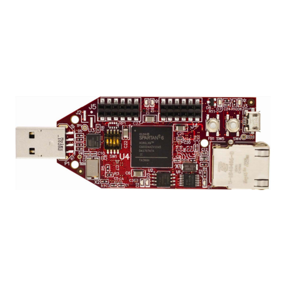
- Page 1 Xilinx® Spartan™-6 LX9 MicroBoard User Guide Revision D...
-
Page 2: Table Of Contents
Ordering Information ..........................7 Functional Description ............................ 8 Xilinx Spartan-6 FPGA LX9 FPGA ......................9 Clocks ..............................11 2.2.1 Triple Output User programmable Texas Instruments CDCE913 clock ........11 ... - Page 3 Figure 8 – PMOD Connector Pinout ........................19 Figure 9 – TPS65708 Connections ........................21 Figure 10 – Xilinx Ribbon Cable JTAG Connector ..................... 24 Tables Table 1 – Ordering Information ..........................7 Table 2 – CDCE913 Clocks ..........................11 ...
-
Page 4: Introduction
FPGA. The installed Spartan-6 FPGA LX9 device offers a prototyping environment to effectively demonstrate the enhanced benefits of low-cost Xilinx FPGA solutions. Reference designs are included with the kit to exercise standard peripherals on the evaluation board for a quick start to device familiarization. -
Page 5: Board Features
1.2 Board Features FPGA o Xilinx Spartan-6 XC6SLX9-2CSG324C FPGA Clocks o Triple Output, user programmable, Texas Instruments CDCE913 clock Pre-programmed during manufacturing Spread-spectrum enabled o Optional user installable Maxim DS1088LU-66+, low-cost, fixed-frequency oscillator Memory o 32 Mb x 16 (512 Mb) Micron LPDDR Mobile SDRAM component o 128 Mb Micron Multi-I/O SPI Flash ... -
Page 6: Reference Designs
1.3 Reference Designs Reference designs that demonstrate some of the potential applications of the Spartan-6 FPGA LX9 MicroBoard are available and can be found on the Avnet Electronics Marketing Design Resource Center (DRC) web site: www.em.avnet.com/s6microboard. See the PDF document included with each reference design for a complete description of the design and detailed instructions for running a demonstration on the development board. -
Page 7: Ordering Information
1.4 Ordering Information The following table lists the evaluation kit part numbers and available software options. Table 1 – Ordering Information Part Number Hardware AES-S6MB-LX9-G Xilinx Spartan-6 FPGA LX9 MicroBoard HW-USB-II-G Xilinx Platform Cable USB-II 210-299P-KIT Digilent HS3 JTAG Cable EF-EDK-NL... -
Page 8: Functional Description
2 Functional Description A Xilinx Spartan-6 FPGA LX9 (XC6SLX9-2CSG324) FPGA is the primary component of the Avnet Spartan-6 FPGA LX9 MicroBoard. A 10/100 Ethernet port and two Full Speed USB interfaces provide means of off- board communication. On-board memory consists of a 256 Mbit x 16 LPDDR mobile SDRAM component and a 128 Mbit Multi-I/O SPI Flash that may be used by the FPGA for configuration. -
Page 9: Xilinx Spartan-6 Fpga Lx9 Fpga
The Xilinx XC6SLX9-2CSG324C device designed onto the Spartan-6 FPGA LX9 MicroBoard is a member of the logic-optimized Xilinx Spartan-6 LX FPGA family. This family is built on a mature 45 nm low-power copper process technology that delivers the optimal balance of cost, power, and performance. The Spartan-6 LX family offers a new, more efficient, dual-register 6-input look-up table (LUT) logic and a rich selection of built-in system-level blocks. -
Page 10: Figure 4 - Xc6Slx9 Csg324 I/O Allocation
2x6 PMODx2 User DIP (4 I/Os) ( 16 I/Os) Bank0 44 IOs (3.3V) LPDDR MCB Bank3 (41 I/Os) Bank1 56 IOs VCCINT Ethernet (18 I/Os) 56 IOs (1.8V) RZQ (1 I/O) (3.3V) Ground User LEDs (4 I/Os) Bank2 44 IOs (3.3V) SPI Flash Clk (1 I/O) -
Page 11: Clocks
2.2 Clocks 2.2.1 Triple Output User programmable Texas Instruments CDCE913 clock The CDCE913 is a modular PLL-based low-cost, high-performance, programmable clock synthesizer, multiplier, and divider. It can generate up to 3 output clocks from a single input frequency. Each output can be programmed via an SDA / SCL, SMBus / I2C interface, for any clock frequency up to 230 MHz, using the integrated configurable PLL. -
Page 12: Memory
2.3 Memory The Spartan-6 FPGA LX9 MicroBoard is populated with both LPDDR mobile SDRAM memory (256 Mbit x 16) and 128 Mbit SPI Multi-I/O Flash to support various types of applications. The SPI Flash may be used for FPGA configuration. Figure 5 shows a high-level block diagram of the memory interfaces on this board. Digilent 4-Pin Flash Progrmming Interface SPI Flash... -
Page 13: Mb X 16 (64Mb) Micron Lpddr Mobile Sdram Component
2.3.1 32 Mb x 16 (64MB) Micron LPDDR Mobile SDRAM component The Micron LPDDR mobile SDRAM device, part number MT46H32M16LFBF-5, provides a double data rate architecture to achieve high-speed operation. The device provides 64 MB and it is internally configured as a quad-bank DRAM of memory on a single IC. -
Page 14: Table 5 - Lpddr Timing Parameters
Table 5 – LPDDR Timing Parameters MT47H16M16BG-5E: Timing Parameters Time (ps) or Number Load Mode Register time (TMRD) 2 tCK Write Recovery time (TWR) 15000 Write-to-Read Command Delay (TWTR) 10000 Delay between ACT and PRE Commands (TRAS) 40000 Delay after ACT before another ACT (TRC) 55000 Delay after AUTOREFRESH Command (TRFC) 75000... -
Page 15: 128 Mb Micron Multi-I/O Spi Flash
Please note that the following patch may be required to build a MicroBlaze Hardware Platform that includes the XPS_SPI peripheral in EDK 12.4 or earlier: http://www.xilinx.com/support/answers/39017.htm Copyright © 2015 Avnet, Inc. AVNET and the AV logo are registered trademarks of Avnet, Inc. All other brands are property of their respective owners. -
Page 16: Communication
The AT90USB162 / ATMEGA162U2 is used to control FPGA configuration via the Digilent JTAG interface and also to directly program the SPI Flash via a Digilent program. JTAG configuration is accomplished using iMPACT and the Digilent Plug-in. Please see the Xilinx Spartan-6 LX9 MicroBoard - Configuration Guide located at www.em.avnet.com/s6microboard... -
Page 17: 10/100 Ethernet Phy Via Texas Instruments Dp83848J Phy And Te Connectivity Rj45 Connector
2.4.3 10/100 Ethernet PHY via Texas Instruments DP83848J PHY and TE Connectivity RJ45 connector The PHY device is a Texas Instruments DP83848J. The TE Connectivity RJ45 connector includes integrated magnetics and LEDs. A MAC must be placed inside the FPGA, such as the AXI Ethernet Lite, AXI Tri-Mode Ethernet Media... -
Page 18: Table 9 - 10/100 Pin Assignments
Table 9 – 10/100 Pin Assignments Net Name FPGA Pin# FPGA_ETH_MDC FPGA_ETH_MDIO FPGA_ETH_RX_CLK FPGA_ETH_RX_D0 FPGA_ETH_RX_D1 FPGA_ETH_RX_D2 FPGA_ETH_RX_D3 FPGA_ETH_RX_ER FPGA_ETH_DV FPGA_ETH_TX_CLK FPGA_ETH_TX_D0 FPGA_ETH_TX_D1 FPGA_ETH_TX_D2 FPGA_ETH_TX_D3 FPGA_ETH_TX_EN FPGA_ETH_COL FPGA_ETH_CRS FPGA_ETH_RESET# Please note that the PHY Address pins are not strapped on the board. The Avnet XBD for this board places pull-ups on the AD[4:1] pins. -
Page 19: User I/O And Expansion Connectors
2.5 User I/O and Expansion Connectors 2.5.1 Peripheral Module (PMOD) Two 12-pin (2 x 6 female) Peripheral Module (PMOD) headers (J4, J5) are interfaced to the FPGA, with each header providing 3.3 V power, ground, and eight I/O’s. These headers may be utilized as general-purpose I/Os or may be used to interface to PMODs. -
Page 20: User Interfaces
2.6 User Interfaces 2.6.1 User LEDs Four discrete “High Brightness, Low Vf ” LED’s are installed on the board and can be used to display the status of the internal logic. These LEDs are attached as shown below and are lit by forcing the associated FPGA I/O pin to a logic ‘1’... -
Page 21: Power
2.7 Power The Texas Instruments TPS65708 provides two high-efficiency switching converters, two LDOs, and an LED driver. The output voltages are tuned internally on the device. The default values are 3.3V and 1.8V for the switchers and 2.8V and 1.2V for the LDOs. In this implementation, the 2.8V LDO output is not utilized. The Spartan-6 FPGA core voltage requires 1.2V. -
Page 22: Fpga Decoupling
2.7.2 FPGA Decoupling The decoupling requirements for the Spartan-6 device are specified in Xilinx UG393 Spartan-6 FPGA PCB Design Guide. The S6LX9 MicroBoard follows the intent of these guidelines with a few variations: A 0.22uF, 6.3V, 0201 package capacitor is used for the smallest capacitor bin rather than 0.47uF. The S6LX9 MicroBoard layout was constrained to using the 0201 package, and 0.22uF was the largest... -
Page 23: Power Results
2.7.3 Power Results The power circuitry was tested during the prototyping phase to verify compliance with the Spartan-6 power requirements, such as: Power rail assignment o Spartan-6 Vccint 1.2 V o Spartan-6 Vccaux 3.3 V o Spartan-6 Vcco_0,_1,_2 3.3 V o Spartan-6 Vcco_3 1.8 V ... -
Page 24: Configuration
The cable is attached to the 14-pin, 2 mm spaced keyed header J4 (Figure 10) with a ribbon cable. Figure 10 – Xilinx Ribbon Cable JTAG Connector Copyright © 2015 Avnet, Inc. AVNET and the AV logo are registered trademarks of Avnet, Inc. All other brands are property of their respective owners. -
Page 25: Test Design
The S6LX9 MicroBoard factory test is programmed into the Micron SPI Flash as part of the functional test ® ® when the boards are built. The results of this test are described in the Xilinx Spartan -6 LX9 MicroBoard Getting Started Guide, the full version of which is available on the DRC. Access to the factory test source archive, including a document describing the factory test procedure, may be granted by contacting your local Avnet/Silica FAE. -
Page 26: Acknowledgements
Avnet would like to acknowledge the following key partners for their key contributions to this project. Atmel (www.atmel.com) USB 2.0 Full Speed USB-to- JTAG bridge via Atmel ATMEGA162U2 Micron (www.micron.com/solutions/partner-ecosystem/xilinx) Multi-I/O SPI Flash LPDDR Memory Texas Instruments (www.ti.com/xilinxfpga) -
Page 27: Getting Help And Support
Avnet Spartan-6 FPGA LX9 MicroBoard forum: http://community.em.avnet.com/t5/Spartan-6-LX9-MicroBoard/bd-p/Spartan-6LX9MicroBoard For Xilinx technical support, you may contact Xilinx Online Technical Support at www.support.xilinx.com. On this site you will also find the following resources for assistance: Software, IP, and Documentation Updates Access to Technical Support Web Tools ... -
Page 28: Revision History
6 Revision History Revision Date Change 2/28/2011 Initial Release Modified Table 10 and Table 11 to reflect PMOD pin order; Changed USER_RESET_N to USER_RESET to reflect actual polarity; Updated TBD references. Changed reference to Factory Test availability on DRC to Avnet/Silica FAE; 7/27/2011 ...
Need help?
Do you have a question about the Spartan-6 LX9 and is the answer not in the manual?
Questions and answers