Table of Contents
Advertisement
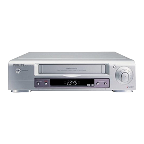
Video Cassette Recorder
Service
Service
Service
Service Manual
Contents
Chapter
Sec. 1:
Adjustment Procedure
Schematic Diagrams and CBA's
Exploded Views
Mechanical and Electrical Parts Lists
Sec. 2: Standard Maintenance
Mechanism Alignment Procedures
Disassembly / Assembly of Mechanism
Deck Exploded Views
Safety regulations require that the set be restored to its original
condition and that parts which are identical with those specified
be used.
Published by BK 2002 Video Service Department Printed in The Netherlands c Copyright reserved
VR530
/02/07/16
Survey of versions:
/02
PAL B/G, VPS/PDC
/07
PAL I, Ireland
/16
PAL B/G, Spain
/39
SECAM L,L' & PAL B/G, I
/58
PAL/SECAM B/G, D/K
Subject to modification GB
3103 785 21990
Advertisement
Chapters
Table of Contents

Subscribe to Our Youtube Channel
Related Manuals for Philips VR 530/07


Summary of Contents for Philips VR 530/07
- Page 1 Video Cassette Recorder Service Service VR530 /02/07/16 Service Service Manual Contents Survey of versions: PAL B/G, VPS/PDC Chapter PAL I, Ireland PAL B/G, Spain Sec. 1: Adjustment Procedure SECAM L,L' & PAL B/G, I Schematic Diagrams and CBA's Exploded Views PAL/SECAM B/G, D/K Mechanical and Electrical Parts Lists Sec.
-
Page 2: Table Of Contents
MAIN SECTION VIDEO CASSETTE RECORDER Sec. 1: Main Section I Adjustment Procedures I Schematic Diagrams and CBA’s I Exploded Views I Mechanical and Electrical Parts List TABLE OF CONTENTS IMPORTANT SAFETY PRECAUTIONS ............1-1-1 STANDARD NOTES FOR SERVICING . - Page 3 SPECIFICATIONS Description Unit Minimum Nominal Maximum Remark 1. Video 1-1. Video Output (PB) Vp-p SP Mode 1-2. Video Output (R/P) Vp-p SP Mode, 1-3. Video S/N Y (R/P) W/O Burst 1-4. Video Color S/N AM (R/P) SP Mode 1-5. Video Color S/N PM (R/P) SP Mode 1-6.
-
Page 4: Important Safety Precautions
IMPORTANT SAFETY PRECAUTIONS Product Safety Notice I. Also check areas surrounding repaired locations. J. Use care that foreign objects (screws, solder drop- Some electrical and mechanical parts have special lets, etc.) do not remain inside the set. safety-related characteristics which are often not evi- K. -
Page 5: Safety Check After Servicing
Safety Check after Servicing Chassis or Secondary Conductor Examine the area surrounding the repaired location for damage or deterioration. Observe that screws, parts, and wires have been returned to their original posi- Primary Circuit Terminals tions. Afterwards, do the following tests and confirm the specified values to verify compliance with safety standards. -
Page 6: Standard Notes For Servicing
STANDARD NOTES FOR SERVICING Circuit Board Indications How to Remove / Install Flat Pack-IC a. The output pin of the 3 pin Regulator ICs is indi- 1. Removal cated as shown. With Hot-Air Flat Pack-IC Desoldering Machine:. (1) Prepare the hot-air flat pack-IC desoldering Top View Bottom View machine, then apply hot air to the Flat Pack-IC... - Page 7 With Soldering Iron: (4) Bottom of the flat pack-IC is fixed with glue to the CBA; when removing entire flat pack-IC, first apply (1) Using desoldering braid, remove the solder from all soldering iron to center of the flat pack-IC and heat pins of the flat pack-IC.
- Page 8 Instructions for Handling 2. Installation Semi-conductors (1) Using desoldering braid, remove the solder from the foil of each pin of the flat pack-IC on the CBA Electrostatic breakdown of the semi-conductors may so you can install a replacement flat pack-IC more occur due to a potential difference caused by electro- easily.
-
Page 9: Function Indicator Symbols
FUNCTION INDICATOR SYMBOLS Note: The following symbols will appear on the indicator panel to indicate the current mode or operation of the VCR. On-screen modes will also be momentarily displayed on the tv screen when you press the operation buttons. Display panel "... -
Page 10: Preparation For Servicing
PREPARATION FOR SERVICING How to Enter the Service Mode About REC-Safety Switch Caution: The REC-Safety Switch is directly mounted on the About Optical Sensors Main CBA. When the Deck Mechanism Assembly is Caution: removed from the Main CBA for servicing, this switch does not work automatically. -
Page 11: Operating Controls And Functions
Buttons with TV feature MUTE To call up additional TV functions. STANDBY/ON To switch VCR or Philips TV on or off, interrupt menu function. INDEX STATUS/EXIT To access or remove the VCR’s on-screen status display. To exit on-screen menus. Or, to access or remove a status display or menu of Philips TV. - Page 12 Front of the device STILL STANDBY/ON PROGRAMME COUNTER RESET RECORD PWR. STANDBY/ON To switch off or on, interrupt a function. PROGRAMME+ PROGRAMME- To select the programme number. During normal or slow motion playback, press to adjust the tracking. RECORD To record the TV channel selected at this moments. When tape playback is stopped, press to fast forward the tape at hight speed.
-
Page 13: Signal Name Abbreviations
SIGNAL NAME ABBREVIATIONS Signal Name Function Signal Name Function DAVN-L VPS/PDC Data Receive = “L” A-MODE Hi-Fi Tape Detection Signal DRV-CLK LED Clock Driver IC Control Clock Audio Mute Control Signal A-MUTE-H DRV-DATA LED Clock Driver IC Control Data (Mute = “H”) LED Clock Driver IC Chip Select Normal Audio Play Back/Record DRV-STB... - Page 14 Signal Name Function P-ON+9V +9V at Power-On Signal P-ON-H Power On Signal at High Video Head Switching Pulse PG-DELAY Signal Adjusted Voltage P-ON Power Detection Input POW-SAF Signal REMOCON-IN Remote Control Sensor System Reset RESET Signal (Reset=”L”) RF-SW Video Head Switching Pulse RGB- SCART 2 RGB Through Control THROUGH...
-
Page 15: Cabinet Disassembly Instructions
CABINET DISASSEMBLY INSTRUCTIONS 1. Disassembly Flowchart (1): Identification (location) No. of parts in the figures (2): Name of the part This flowchart indicates the disassembly steps to gain (3): Figure Number for reference access to item(s) to be serviced. When reassembling, (4): Identification of parts to be removed, unhooked, follow the steps in reverse order. - Page 16 (S-1) (S-1) (S-4) (S-3) (S-3) (S-5) [3]VCR (S-4) Chassis Unit (S-3) [1] Top Case (S-2) (S-1) Fig. 1 (L-2) (L-3) (L-2) Fig. 3 [4] Jack CBA (S-6) [2] Front Desolder Assembly (L-1) Fig. 2 Fig. 4 1-7-2 HC460DC...
- Page 17 FE Head Cylinder Assembly AC Head Assembly SW507 LD-SW [7] Main CBA [6] Deck Assembly [6] Deck Assembly [7] Main CBA Cam Gear (S-7) Hole Shaft Hole [5] Function LD-SW (S-7) [7] Main CBA Desolder from bottom Fig. 6 From From From Capstan Motor...
-
Page 18: Electrical Adjustment Instructions
ELECTRICAL ADJUSTMENT INSTRUCTIONS General Note: "CBA" is an abbreviation for Head Switching Position Adjustment "Circuit Board Assembly." Purpose: NOTE: To determine the Head Switching point during 1.Electrical adjustments are required after replacing playback. circuit components and certain mechanical parts. Symptom of Misadjustment: It is important to do these adjustments only after all repairs and replacements have been com- May cause Head Switching noise or vertical jitter... - Page 19 How to enter the factory How to measure the standard V- set mode ENV value of Digital Studio Picture Control In the factory set mode, measuring the standard V- ENV value of Digital Studio Picture Control can be per- 1. To enter the measuring the standard V-ENV value formed.
- Page 20 Adjustment Points and Test Points Main CBA Top View AUDIO BLOCK POWER SUPPLY BLOCK VIDEO TUNER BLOCK BLOCK TP751 V-OUT TP507 SYSCON/TIMER POWER SENS-INH SERVO BLOCK TP501 CTL BLOCK TP502 RF-SW TP301 C-PB VR501 SW-P TEST POINT INFORMATION : Indicates a test point with a jumper wire across a hole in the PCB. TEST POINTS NOT USED IN ELECTRICAL ADJUSTMENTS Test Point Used in:...
-
Page 21: Block Diagrams
BLOCK DIAGRAMS Servo/System Control Block Diagram NOTE FOR WIRE CONNECTORS: TEST POINT INFORMATION 1. PREFIX SYMBOL "CN" MEANS CONNECTOR. :INDICATES A TEST POINT WITH A JUMPER WIRE ACROSS A HOLE IN THE PCB. (CAN DISCONNECT AND RECONNECT.) :USED TO INDICATE A TEST POINT WITH A COMPONENT LEAD ON FOIL SIDE. 2. -
Page 22: Video Block Diagram
Video Block Diagram NOTE FOR WIRE CONNECTORS: TEST POINT INFORMATION 1. PREFIX SYMBOL "CN" MEANS CONNECTOR. :INDICATES A TEST POINT WITH A JUMPER WIRE ACROSS A HOLE IN THE PCB. (CAN DISCONNECT AND RECONNECT.) :USED TO INDICATE A TEST POINT WITH A COMPONENT LEAD ON FOIL SIDE. 2. -
Page 23: Audio Block Diagram
Audio Block Diagram NOTE FOR WIRE CONNECTORS: TEST POINT INFORMATION 1. PREFIX SYMBOL "CN" MEANS CONNECTOR. :INDICATES A TEST POINT WITH A JUMPER WIRE ACROSS A HOLE IN THE PCB. (CAN DISCONNECT AND RECONNECT.) :USED TO INDICATE A TEST POINT WITH A COMPONENT LEAD ON FOIL SIDE. 2. - Page 24 Hi-Fi Audio Block Diagram NOTE FOR WIRE CONNECTORS: TEST POINT INFORMATION 1. PREFIX SYMBOL "CN" MEANS CONNECTOR. :INDICATES A TEST POINT WITH A JUMPER WIRE ACROSS A HOLE IN THE PCB. (CAN DISCONNECT AND RECONNECT.) :USED TO INDICATE A TEST POINT WITH A COMPONENT LEAD ON FOIL SIDE. 2.
- Page 25 Power Supply Block Diagram NOTE : CAUTION CAUTION ! Fixed voltage (or Auto voltage selectable ) power supply circuit is used in this unit. The voltage for parts in hot circuit is measured using FOR CONTINUED PROTECTION AGAINST FIRE HAZARD, If Main Fuse (F001) is blown, check to see that all components in the power supply REPLACE ONLY WITH THE SAME TYPE T1.6AL/250V FUSE.
-
Page 26: Schematic Diagrams / Cba's And Test Points
SCHEMATIC DIAGRAMS / CBA'S AND TEST POINTS Main 1/5 Schematic Diagram Parts Location Guide Standard Notes Notes: Ref No. Position Ref No. Position Ref No. Position Ref No. Position WARNING 1. Do not use the part number shown on these draw- CAPACITORS CONNECTORS RESISTORS... - Page 27 Main 1/5 Schematic Diagram Comparison Chart of MODE: SP/REC PLAY MODE Models and Marks REC MODE (2.5) MODEL MARK INDICATES THAT THE VOLTAGE THE SAME VOLTAGE FOR VR530/02 BOTH PLAY & REC MODES. IS NOT CONSISTENT HERE. VR530/07 “ “ = SMD VR530/16 IC501 KEY VOLTAGE CHART Pin No.
- Page 28 Main 2/5 Schematic Diagram Comparison Chart of MODE: SP/REC Models and Marks PLAY MODE REC MODE MODEL MARK (2.5) INDICATES THAT THE VOLTAGE VR530/02 THE SAME VOLTAGE FOR BOTH PLAY & REC MODES. IS NOT CONSISTENT HERE. VR530/07 “ “ = SMD VR530/16 1-10-6 1-10-7...
- Page 29 MAIN 3/5 Schematic Diagram Parts Location Guide MAIN 2/5 Schematic Diagram Parts Location Guide Ref No. Position Ref No. Position Ref No. Position Ref No. Position Ref No. Position CAPACITORS CAPACITORS CAPACITORS TRANSISTORS RESISTORS C157 C251 C352 Q401 R403 C158 C252 C401 Q402...
- Page 30 Main 3/5 Schematic Diagram MODE: SP/REC PLAY MODE REC MODE (2.5) INDICATES THAT THE VOLTAGE THE SAME VOLTAGE FOR BOTH PLAY & REC MODES. IS NOT CONSISTENT HERE. “ “ = SMD 1-10-11 1-10-12 1-10-13 HC460SCM3...
- Page 31 Main 4/5 Schematic Diagram Comparison Chart of Models and Marks MODEL MARK VR530/02 VR530/07 VR530/16 NOTE : CAUTION ! MODE: SP/REC PLAY MODE REC MODE THE VOLTAGE FOR PARTS IN HOT CIRCUIT IS MEASURED USING Fixed voltage (or Auto voltage selectable ) power supply circuit is used in this unit. (2.5) HOT GND AS A COMMON TERMINAL.
- Page 32 Main 5/5 Schematic Diagram MODE: SP/REC “ “ = SMD PLAY MODE REC MODE (2.5) INDICATES THAT THE VOLTAGE THE SAME VOLTAGE FOR IS NOT CONSISTENT HERE. BOTH PLAY & REC MODES. MAIN 5/5 Schematic Diagram Parts Location Guide Ref No. Position Ref No.
- Page 33 Function Schematic Diagram Function Schematic Diagram Parts Location Guide Ref No. Position Ref No. Position CONNECTORS SWITCHES CN651 SW651 RESISTORS SW652 R651 SW653 R652 SW654 R653 SW656 R654 R655 HC460SCF MODE: SP/REC PLAY MODE VPS Schematic Diagram REC MODE (2.5) THE SAME VOLTAGE FOR INDICATES THAT THE VOLTAGE BOTH PLAY &...
- Page 34 AFV Schematic Diagram Comparison Chart of MODE: SP/REC PLAY MODE Models and Marks REC MODE (2.5) MODEL MARK INDICATES THAT THE VOLTAGE THE SAME VOLTAGE FOR VR530/02 BOTH PLAY & REC MODES. IS NOT CONSISTENT HERE. VR530/07 “ “ = SMD VR530/16 AFV Schematic Diagram Parts Location Guide...
- Page 35 Jack Schematic Diagram MODE: SP/REC PLAY MODE REC MODE (2.5) INDICATES THAT THE VOLTAGE THE SAME VOLTAGE FOR BOTH PLAY & REC MODES. IS NOT CONSISTENT HERE. “ “ = SMD JACK Schematic Diagram Parts Location Guide Ref No. Position Ref No.
- Page 36 Main CBA Top View CAUTION ! BECAUSE A HOT CHASSIS GROUND IS PRESENT IN THE POWER Fixed voltage (or Auto voltage selectable ) power supply circuit is used in this unit. SUPPLY CIRCUIT , AN ISOLATION TRANSFORMER MUST BE USED. ALSO , IN ORDER TO HAVE THE ABILITY TO INCREASE THE INPUT CAUTION If Main Fuse (F001) is blown, check to see that all components in the power supply...
- Page 37 Main CBA Bottom View CAUTION ! BECAUSE A HOT CHASSIS GROUND IS PRESENT IN THE POWER Fixed voltage (or Auto voltage selectable ) power supply circuit is used in this unit. SUPPLY CIRCUIT , AN ISOLATION TRANSFORMER MUST BE USED. ALSO , IN ORDER TO HAVE THE ABILITY TO INCREASE THE INPUT CAUTION If Main Fuse (F001) is blown, check to see that all components in the power supply...
- Page 38 Main CBA Top View CAUTION ! BECAUSE A HOT CHASSIS GROUND IS PRESENT IN THE POWER SUPPLY CIRCUIT , AN ISOLATION TRANSFORMER MUST BE USED. Fixed voltage (or Auto voltage selectable ) power supply circuit is used in this unit. ALSO , IN ORDER TO HAVE THE ABILITY TO INCREASE THE INPUT CAUTION NOTE :...
- Page 39 Main CBA Bottom View BECAUSE A HOT CHASSIS GROUND IS PRESENT IN THE POWER CAUTION ! SUPPLY CIRCUIT , AN ISOLATION TRANSFORMER MUST BE USED. Fixed voltage (or Auto voltage selectable ) power supply circuit is used in this unit. ALSO , IN ORDER TO HAVE THE ABILITY TO INCREASE THE INPUT CAUTION NOTE :...
- Page 40 Main CBA Parts Location Guide Ref No. Position Ref No. Position Ref No. Position Ref No. Position Ref No. Position Ref No. Position Ref No. Position Ref No. Position Ref No. Position CAPACITORS CAPACITORS CAPACITORS CAPACITORS COILS RESISTORS RESISTORS RESISTORS RESISTORS C002 C338...
- Page 41 Function CBA Top View Function CBA Bottom View Function CBA Top View Function CBA Bottom View NOTE : Either BHC400F01013, BHC400F01014 is used for the Function CBA in this S/M. BHC400F01013-B BHC400F01014-B Function CBA Parts Location Guide Ref No. Position Ref No.
- Page 42 Power SW CBA Top View Power SW CBA Bottom View Power SW CBA Top View Power SW CBA Bottom View NOTE : Either BHC400F01013, BHC400F01014 is used for the Power SW CBA in this S/M. BHC400F01013-D BHC400F01014-D 1-10-41 1-10-42...
- Page 43 AFV CBA Top View AFV CBA Bottom View AFV CBA Parts Location Guide Ref No. Position Ref No. Position CAPACITORS CONNECTORS DIODES COILS RESISTORS CRYSTAL OSCILLATORS BHC400F01091 1-10-43 1-10-44...
- Page 44 VPS CBA Top View VPS CBA Bottom View VPS CBA Top View VPS CBA Bottom View NOTE : Either BHC400F01013, BHC400F01014 is used for the Vps CBA in this S/M. BHC400F01013-C BHC400F01014-C VPS CBA Parts Location Guide Ref No. Position CAPACITORS C640 C642...
- Page 45 Jack CBA Top View NOTE : Either BHC400F01013, BHC400F01014 is used for the Jack CBA in this S/M. JACK CBA Parts Location Guide Ref No. Position Ref No. Position CAPACITORS TRANSISTORS C101 Q102 C102 RESISTORS C103 R101 C104 R103 C105 R104 C106 R106...
- Page 46 Jack CBA Top View NOTE : Either BHC400F01013, BHC400F01014 is used for the Jack CBA in this S/M. Jack CBA Bottom View BHC400F01014-E 1-10-49 1-10-50...
-
Page 47: Waveforms
WAVEFORMS (TP751 of Main CBA) V-OUT E-E 10usec 50mV x 10 (TP751 of Main CBA) UPPER (TP302 of Main CBA) LOWER V-OUT 0.1V x 10 RF-SW 0.5V x 10 50usec (TP301 of Main CBA) UPPER (TP302 of Main CBA) LOWER C-PB 10mV x 10 RF-SW... -
Page 48: Wiring Diagram
WIRING DIAGRAM NOTE FOR WIRE CONNECTORS: 1. PREFIX SYMBOL "CN" MEANS CONNECTOR. AC CORD (CAN DISCONNECT AND RECONNECT.) 2. PREFIX SYMBOL "CL" MEANS WIRE-SOLDER HOLES OF THE PCB. (WIRE IS SOLDERED DIRECTLY.) ANT-IN ANT-OUT CN701 SENSOR CBA 1 NU (BHB300F01011) 3 GND TU-AUDIO(R) AFV CBA... -
Page 49: System Control Timing Charts
SYSTEM CONTROL TIMING CHARTS Mode SW : LD-SW LD-SW Position detection A/D Input voltage Limit Symbol (Calculated voltage) 3.76V~4.50V (4.12V) 4.51V~5.00V (5.00V) 0.00V~0.25V (0.00V) 1.06V~1.50V (1.21V) 0.66V~1.05V (0.91V) 1.99V~2.60V (2.17V) 1.51V~1.98V (1.80V) 3.20V~3.75V (3.40V) 0.26V~0.65V (0.44V) 4.51V~5.00V (5.00V) 2.61V~3.19V (2.97V) Note : EJ RS : Loading FWD (LM-FWD “H”, LM-REV “L”) RS EJ : Loading REV (LM-FWD “L”, LM-REV “H”) - Page 50 13 RF-SW The first rise of RF-SW after a rise in F-AD signal F-AD (Internal Signal) "H" "H" "Z" 5 C-DRIVE "L" "L" Stop detection (T2) Acceleration Detection (T1) Slow Tracking Value 37 PB CTL Reversal Limit Value 10 C-F/R 11 H-A-SW 12 ROTA STILL...
- Page 51 13 RF-SW The first rise of RF-SW after a rise in F-AD signal F-AD (Internal Signal) "H" "H" "Z" 5 C-DRIVE "L" "L" Stop detection (T2) Acceleration Detection (T1) Slow Tracking Value 37 PB CTL Reversal Limit Value 10 C-F/R 11 H-A-SW 12 ROTA STILL...
- Page 52 EJECT ST-S,/ END-S "OFF" CASS.LOAD LD-FWD 0.2S LD-REV 0.7S LD-FWD 0.2S LD-REV 0.2S LD-FWD 0.5S LD-REV STOP(A) PLAY LD-FWD PLAY LD-FWD LD-REV 0.2S LD-FWD PLAY PLAY PAUSE (SLOW) LD-FWD STILL(SLOW) PLAY LD-REV 0.2S LD-FWD PLAY STOP /EJECT LD-REV STOP(A) Fig. 3 1-13-4 HC460TI...
- Page 53 STOP(A) STOP LD-REV 0.2S LD-FWD STOP /EJECT LD-REV 2.0S LD-FWD 0.5S LD-REV STOP(A) LD-REV 0.2S LD-FWD STOP /EJECT LD-REV 2.0S LD-FWD 0.5S LD-REV STOP(A) LD-FWD PAUSE LD-FWD 2.5S Short REV LD-REV 0.2S LD-FWD REC PAUSE REC or PAUSE STOP /EJECT LD-FWD 1.5S LD-REV...
-
Page 54: Ic Pin Function Descriptions
IC PIN FUNCTION DESCRIPTIONS IC501( SERVO / SYSTEM CONTROL IC ) Signal Active Function Name Level “H” ≥ 4.5V, “L” ≤ 1.0V N.U. Not Used Signal Active Function Name Level N.U. Not Used Input Signal from SCART 2 RGB SC2-IN L/Hi-z 27 OUT RGB- Pin 8 of SCART2... - Page 55 Signal Active Signal Active Function Function Name Level Name Level Composite CTL Amp Gain C-SYNC PULSE 84 OUT FF/REW- Synchronized Pulse Switching Signal (FF/ REW=”L”) 59 OUT 8POUT-1 SCART 1 8Pin Output Control Signal N.U. Not Used 60 OUT 8POUT-2 SCART 2 8Pin P-DOWN- Power Voltage Down Output Control Signal...
-
Page 56: Lead Identifications
LEAD IDENTIFICATIONS 2SC1815-Y(TPE2) LM339DT BN1F4M-T 2SC1815-GR(TPE2) KIA339F EL BA1F4M-T 2SC3266-Y (TPE2) KTA1266(GR) KTA1271(Y) KTC3199(Y,GR,BL) 2SC2120-Y(TPE2) 2SC2785(J.H.F.K) KTC3203(Y) KRA103M 2SC1815-BL(TPE2) KRC103M 2SA1020(Y) 2SA1015-GR(TPE2) 2SB892(S) KRA104M KTC3205(Y) 2SD1246(S,T) LA71750AM-MTB E C B E C B QSZAD0RMB100 BR24C04F-W AT24C04N-10SC LTV-817(B.C)-F M24C04-MN6 EL817(A,B,C) LA72646M FS1KM-18A FS1KM-14A LC74793JM-TRM... -
Page 57: Electrical Parts List
ELECTRICAL PARTS LIST ELECTRICAL PARTS LIST Pos. 12 NC Description Pos. 12 NC Description X36F MCV CBA C342 ELECTROLYTIC CAP. 1UF/50V M H7 X36F MCV CBA C343 CHIP CERAMIC CAP. F Z 0.1UF/50V X36F MCV CBA C344 CERAMIC CAP.(AX) B K 100PF/50V Consists of the following C345 CHIP CERAMIC CAP. - Page 58 ELECTRICAL PARTS LIST ELECTRICAL PARTS LIST Pos. 12 NC Description Pos. 12 NC Description C518 CHIP CERAMIC CAP. B K 0.047UF/50V D552 4822 130 10094 ZENER DIODE MTZJT-777.5A C519 CHIP CERAMIC CAP. B K 0.01UF/50V D553 4822 130 30621 SWITCHING DIODE 1N4148M C520 CHIP CERAMIC CAP.
- Page 59 ELECTRICAL PARTS LIST ELECTRICAL PARTS LIST Pos. 12 NC Description Pos. 12 NC Description R012 CARBON RES. 1/4W J 390K OHM R413 CHIP RES.(1608) 1/10W J 330K OHM R013 CARBON RES. 1/6W J 470K OHM R414 CHIP RES.(1608) 1/10W J 120 OHM R014 CARBON RES.
- Page 60 ELECTRICAL PARTS LIST ELECTRICAL PARTS LIST Pos. 12 NC Description Pos. 12 NC Description R544 CHIP RES.(1608) 1/10W J 1.5K OHM X502 9965 000 12288 X’TAL 32.768KHZ(20PPM) R545 CHIP RES.(1608) 1/10W J 2.2K OHM FUNCTION CBA R546 CHIP RES.(1608) 1/10W J 1.8K OHM CN651 9965 000 09213 ANGLE PIN HEADER R547...
- Page 61 ELECTRICAL PARTS LIST ELECTRICAL PARTS LIST Pos. 12 NC Description Pos. 12 NC Description R119 CHIP RES.(1608) 1/10W J 75 OHM ELECTROLYTIC CAP. 10UF/16V M H7 R120 CARBON RES. 1/6W J 680 OHM CHIP CERAMIC CAP. F Z 0.1UF/50V R123 CHIP RES.(1608) 1/10W J 220 OHM CHIP CERAMIC CAP.
-
Page 62: Exploded Views
EXPLODED VIEWS Front Panel 1-17-1 HC460FEX... - Page 63 Cabinet 2L011 2B18 2L011 2L011 2L011 2L011 JACK CBA 2L012 2L042 2L021 2L021 2L022 2L021 2L051 2L021 2L022 2L022 2L022 2L021 SENSOR CBA 2L041 VPS CBA AFV CBA POWER SW CBA MAIN CBA 2L031 SENSOR CBA 2L041 2L031 2L043 2B46 FUNCTION CBA 1-17-2 HB460CEX...
- Page 64 Packing Comparison Chart of Some Ref. Numbers are not in sequence. Models and Marks Model Mark X36A VR530/02 [ A, C ] VR530/07 X36B X36C VR530/16 [ A, C ] [ C ] [ C ] X20A X20B X20C X20D X20E X20F X36F...
-
Page 65: Mechanical Parts List
MECHANICAL PARTS LIST Pos. 12 NC Description 9965 000 12280 FRONT ASSEMBLY HC460ED 9965 000 12292 FRONT ASSEMBLY HC462ED 9965 000 12164 CASE, TOP HC460ED 9965 000 12165 CHASSIS HC461BD 9965 000 12166 PANEL, BOTTOM HC461BD LABEL, RATING HC460ED LABEL, RATING HC461BD LABEL, RATING HC462ED LABEL, BAR CODE HC460ED LABEL, BAR CODE HC461BD... - Page 66 DECK MECHANISM SECTION VIDEO CASSETTE RECORDER Sec. 2: Deck Mechanism Section I Standard Maintenance I Mechanism Alignment Procedures I Disassembly / Assembly of Mechanism I Deck Exploded Views I Deck Parts List TABLE OF CONTENTS STANDARD MAINTENANCE ............. . 2-1-1 SERVICE FIXTURE AND TOOLS .
-
Page 67: Standard Maintenance
STANDARD MAINTENANCE Service Schedule of Components H: Hours : Check I: Change Deck Periodic Service Schedule Ref.No. Part Name 1,000 H 2,000 H 3,000 H 4,000 H Cylinder Assembly Loading Motor Assembly Pulley Assembly Tension Lever Sub Assembly AC Head Assembly B573,B574 Reel S, Reel T Capstan Motor... - Page 68 Cleaning Cleaning of Audio Control Head Clean the head with a cotton swab. Cleaning of Video Head Procedure Clean the head with a head cleaning stick or chamois 1.Remove the top cabinet. cloth. 2.Dip the cotton swab in 90% isopropyl alcohol and Procedure clean the audio control head.
-
Page 69: Service Fixture And Tools
SERVICE FIXTURE AND TOOLS J-1-1, J-1-2 Ref. No. Name Part No. Adjustment J-1-1 Alignment Tape 4822 395 10283 Electrical Adjustments J-1-2 Alignment Tape 4822 395 10057 Azimuth and X Value Adjustment of Audio Control Head / Adjustment of Envelope Waveform Guide Roller Adj.Screwdriver Available Guide Roller... -
Page 70: Mechanical Alignment Procedures
MECHANICAL ALIGNMENT PROCEDURES Explanation of alignment for the tape to correctly run B. Method to place the Cassette Holder in the tape- starts on the next page. Refer to the information below loaded position without a cassette tape on this page if a tape gets stuck, for example, in the 1. - Page 71 1.Tape Interchangeability Alignment Note: To do these alignment procedures, make sure that the Tracking Control Circuit is set to the center position every time a tape is loaded or unloaded. (Refer to page 2-3-4, procedure 1-C, step 2.) Equipment required: Dual Trace Oscilloscope VHS Alignment Tape (4822 395 10057) Guide Roller Adj.
- Page 72 1-A. Preliminary/Final Checking and 3. Check to see that the tape runs without creasing at Alignment of Tape Path Take-up Guide Post [4] or without snaking between Guide Roller [3] and AC Head. (Fig. M3 and M5) Purpose: 4. If creasing or snaking is apparent, adjust the Tilt To make sure that the tape path is well stabilized.
- Page 73 6. Press CH DOWN button on the unit until the CTL 1-D. Azimuth Alignment of Audio/Control/ waveform has shifted from its original position (not Erase Head the position achieved in step 5, but the position of Purpose: CTL waveform in step 4) by approximately -2msec. To correct the Azimuth alignment so that the Audio/ Make sure that the envelope is simply attenuated Control/Erase Head meets tape tracks properly.
-
Page 74: Disassembly/Assembly Procedures Of Deck Mechanism
DISASSEMBLY/ASSEMBLY PROCEDURES OF DECK MECHANISM Before following the procedures described below, be sure to remove the deck assembly from the cabinet. (Refer to CABINET DISASSEMBLY INSTRUCTIONS on page 1-7-1.) All the following procedures, including those for adjustment and replacement of parts, should be done in Eject mode;... - Page 75 REMOVAL INSTALLATION STEP START- REMOVE/*UNHOOK/ /LOC. PART ADJUSTMENT Fig. No. UNLOCK/RELEASE/ CONDITION UNPLUG/DESOLDER Loading Arm S(B) (+)Refer to Alignment [35] [25] DM2,DM15 Assembly Sec.Pg.2-4-9 Loading Arm T(B) (+)Refer to Alignment [36] [35] DM2,DM15 Assembly Sec.Pg.2-4-9 [37] [2],[25] M Brake T(HI) Assembly DM1,DM16 *(P-6) [38] [2],[25] M Brake S(HI) Assembly...
- Page 76 Top View [45] [46] [50] [47] [14] [13] [11] [15] [39] [40] [10] [12] [38] [37] [44] [33] [42] [31] [32] [41] [43] Fig. DM1 Bottom View [19] [36] [35] [24] [26] [27] [25] [23] [28] [22] [29] [20] [34] Fig.
- Page 77 (S-1) (S-1) (S-2) (P-1) (S-4) (S-3) Fig. DM5 Fig. DM3 [50] Pin D Pin C Pull up Slide (L-8) Pin A Pin B Slot A (S-5) Slots B Slot A First, while pushing the locking tab as shown in the right, slide and pull up the right side on [2] to release Pin A and Pin B from the slots A.
- Page 78 (S-7) (S-9) [14] (S-10) [15] Desolder from bottom (S-6) Lead with White Stripe Belt View for A Fig. DM7 Fig. DM9 (L-2) Adj. Screw [17] After removing the Screw (S-11), [11] while pressing the Locking Tab (L-3) (L-1) (L-3), remove [16]. [16] (P-3) [13]...
- Page 79 Cap Belt (C-1) [20] [19] [21] Fig. DM12 (S-12) Fig. DM11 2-4-6 HC460DA...
- Page 80 [25] (C-5) (C-2) (C-3) [22] [23] (S-15) [26] (L-4) (P-4) [27] (C-6) [29] (C-4) [28] [30] [24] [31] (P-4) [28] [32] When installing [23], install the spring (P-4) to [28] as Position of Mode Lever when installed shown in the left figure, and Pin of [38] then install [23] while Pin on...
- Page 81 Refer to the Alignment Section, Page 2-4-9. [46] [45] [47] (P-5) (L-7) [34] [33] [36] [35] (L-5) Fig. DM17 Fig. DM15 [39] (C-8) [42] (C-7) (P-7) [44] [41] turn (L-6) [43] [48] [49] Slide (P-6) [38] turn [37] [40] Fig. DM18 turn Fig.
-
Page 82: Alignment Procedures Of Mechanism
ALIGNMENT PROCEDURES OF MECHANISM The following procedures describe how to align the Alignment 1 individual gears and levers that make up the tape Loading Arm, S and T Assembly loading/unloading mechanism. Since information about the state of the mechanism is provided to the Install Loading Arm S and T Assembly so that their System Control Circuit only through the Mode Switch, triangle marks point to each other as shown in Fig. - Page 83 Alignment 3 Cam Gear (A), Rack Assembly Install the Rack Assembly so that the first tooth on the gear of the Rack Assembly meets the first groove on the Cam Gear (A) as shown in Fig. AL4. Top View Cam Gear (A) Alignment 3 First tooth First groove...
-
Page 84: Deck Exploded Views
DECK EXPLODED VIEWS Deck Mechanism View 1 Mark Description Part No. (Blue grease) Floil G-374G 0VZZ00109 SLIDUS OIL #150 0VZZ00226 L1467 B494 B553 L1191 B411 B567 L1053 B410 L1051 Chassis Assembly Top View (Lubricating Point) B501 B560 L1450 B426 L1466 B121 B126 L1468... - Page 85 Deck Mechanism View 2 Mark Description Part No. Floil G-374G (Blue grease) 0VZZ00109 B574 B487 B508 B148 B499 B573 L1406 B522 B518 B520 B521 B414 B564 B585 B558 B572 B557 B416 B565 B417 B525 B568 L1151 B551 B584 B578 B579 B582 B580 B569...
- Page 86 Deck Mechanism View 3 Mark Description Part No. Floil G-374G (Blue grease) 0VZZ00109 L1321 B347 L1321 B355 B354 B483 B529 B425 L1461 B360 L1341 B359 B482 B562 L1341 B300 B563 B555 B303 Some Ref. Numbers are not in sequence. B514 2-5-3 HC460DEX...
-
Page 87: Deck Parts List
DECK PARTS LIST DECK PARTS LIST Pos. 12 NC Description Pos. 12 NC Description 9965 000 12201 CYLINDER ASS. MK11 PAL 4HD HIFI B522 9965 000 08483 TG POST ASSEMBLY MK10 9965 000 12202 LOADING MOTOR ASSEMBLY MK11 9965 000 12230 LDG BELT MK11 B525 9965 000 12203...
Need help?
Do you have a question about the VR 530/07 and is the answer not in the manual?
Questions and answers