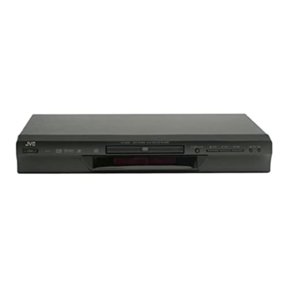
JVC XV-S300BK Service Manual
Dvd video player
Hide thumbs
Also See for XV-S300BK:
- Instructions manual (156 pages) ,
- Service manual (78 pages) ,
- (54 pages)
Table of Contents
Advertisement
Quick Links
SERVICE MANUAL
XV-S300BK / XV-S302SL
STANDBY/ON
OPEN/
CLOSE
1
2
3
4
5
6
7
8
9
10
0
+10
RETURN
CANCEL
ENTER
PREVIOUS
NEXT
CLEAR
SELECT
STROBE
SLOW
-
SLOW
+
PLAY
THEATER
MODE
SUB TITLE
AUDIO
POSITION
3D
PHONIC DIGEST
ANGLE
ZOOM
STANDBY/ON
RM-SXV001A
REMOTE CONTROL
Contents
Safety precautions ------------------------ 1-2
Preventing static electricity ------------- 1-3
Precautions for service ------------------ 1-4
Important for laser products ------------ 1-5
Disassembly method --------------------- 1-6
DVD VIDEO PLAYER
DVD/SUPER VCD/VCD/CD PLAYER
STANDBY
DOLBY
D I G I T A L
Each difference point
Model
XV-S300BK
XV-S302SL
This service manual is printed on 100% recycled paper.
COPYRIGHT
2002 VICTOR COMPANY OF JAPAN, LTD.
XV-S300BK/XV-S302SL
B --------------------------- U.K.
E ----- Continental europe
EN ------ Northern europe
EV ------- Eastern Europe
EE -- Russian Federation
OPEN/CLOSE
STOP
PLAY
PAUSE
Body color
Black
Silver
Adjustment method ----------------------- 1-15
Attention when pick-up is exchanged - 1-19
Comfirm method of operation ---------- 1-20
Troubleshooting --------------------------- 1-21
Description of major ICs ----------------- 1-25
Area Suffix
SKIP
No.A0029
Apr. 2002
Advertisement
Table of Contents

Subscribe to Our Youtube Channel
Related Manuals for JVC XV-S300BK


Summary of Contents for JVC XV-S300BK
- Page 1 XV-S300BK/XV-S302SL SERVICE MANUAL DVD VIDEO PLAYER XV-S300BK / XV-S302SL Area Suffix B --------------------------- U.K. E ----- Continental europe EN ------ Northern europe EV ------- Eastern Europe EE -- Russian Federation STANDBY/ON OPEN/ CLOSE RETURN CANCEL ENTER PREVIOUS NEXT CLEAR SELECT...
- Page 2 XV-S300BK/XV-S302SL 1. This design of this product contains special hardware and many circuits and components specially for safety purposes. For continued protection, no changes should be made to the original design unless authorized in writing by the manufacturer. Replacement parts must be identical to those used in the original circuits. Services should be performed by qualified personnel only.
-
Page 3: Preventing Static Electricity -------------
XV-S300BK/XV-S302SL Preventing static electricity Electrostatic discharge (ESD), which occurs when static electricity stored in the body, fabric, etc. is discharged, can destroy the laser diode in the traverse unit (optical pickup). Take care to prevent this when performing repairs. 1.1. Grounding to prevent damage by static electricity Static electricity in the work area can destroy the optical pickup (laser diode) in devices such as DVD players. -
Page 4: Precautions For Service ------------------
XV-S300BK/XV-S302SL Precautions for service Handling of Traverse Unit and Laser Pickup 1. Do not touch any peripheral element of the pickup or the actuator. 2. The traverse unit and the pickup are precision devices and therefore must not be subjected to strong shock. -
Page 5: Important For Laser Products ------------
XV-S300BK/XV-S302SL Important for laser products 5.CAUTION : If safety switches malfunction, the laser is able 1.CLASS 1 LASER PRODUCT to function. 2.DANGER : Invisible laser radiation when open and inter 6.CAUTION : Use of controls, adjustments or performance of lock failed or defeated. Avoid direct exposure to beam. -
Page 6: Disassembly Method ---------------------
XV-S300BK/XV-S302SL Disassembly method <Main body> Removing the top cover (see Fig.1) Remove the two screws A attaching the top cover on both sides of the body. A x 2 Remove the three screws B attaching the top cover on the back of the body. -
Page 7: Xv-S300Bk/Xv-S302Sl
XV-S300BK/XV-S302SL Removing the rear panel (see Fig.5) *Prior to performing the following procedure, remove Rear panel the top cover. 1.Remove the eight screws E attaching the rear panel on the back of the body. Fig.5 Hook d Hook c Removing the front panel assembly Front panel (see Fig.6,7) -
Page 8: Xv-S300Bk/Xv-S302Sl
XV-S300BK/XV-S302SL <Loading assembly section> Removing the clamper assembly Joint a Joint a (See Fig.1) Remove the four screws A attaching the clamper assembly. Move the clamper in the direction of the arrow to release the two joints a on both sides. -
Page 9: Xv-S300Bk/Xv-S302Sl
XV-S300BK/XV-S302SL Removing the traverse mechanism assembly (See Fig.4 and 5) Prior to performing the following procedure, remove the clamper assembly and the tray. Traverse mechanism Remove the four screws B attaching the traverse assembly mechanism assembly. ATTENTION: Before reattaching the traverse... -
Page 10: Xv-S300Bk/Xv-S302Sl
XV-S300BK/XV-S302SL Removing the motor assembly (See Fig.8 and 9) Belt Prior to performing the following procedure, remove the clamper assembly, the tray, the traverse mechanism assembly and the elevator. Remove the belt from the pulley. Remove the screw C attaching the motor assembly. -
Page 11: Xv-S300Bk/Xv-S302Sl
XV-S300BK/XV-S302SL Pulley gear Idle gear Pulley gear bracket Pulley gear Idle gear Pulley gear bracket Tads h Pulley gear Motor assembly Fig.10 Slide cam Removing the Idle gear / pulley gear / middle gear / slide cam (See Fig.10 to 12) -
Page 12: Xv-S300Bk/Xv-S302Sl
XV-S300BK/XV-S302SL <Traverse mechanism assembly section> Feed motor assembly Removing the feed motor assembly (See Fig.13) Unsolder the two soldering j on the spindle motor board. Remove the two screws F attaching the feed motor assembly. Pickup Notch k Soldering j... -
Page 13: Xv-S300Bk/Xv-S302Sl
XV-S300BK/XV-S302SL Removing the pickup (See Fig.16 and 17) Pickup Joint n Remove the screw I attaching the T spring (S) and Shaft holder the shaft holder. Remove also the plate. ATTENTION: When reattaching, make sure that the T spring (S) presses the shaft. -
Page 14: Xv-S300Bk/Xv-S302Sl
XV-S300BK/XV-S302SL Spindle motor Removing the spindle motor assembly (See Fig.19 to 21) Remove the three screws L attaching the spindle motor on the bottom of the mechanism base. ATTENTION: When reattaching, pass the card wire extending from the spindle motor board through the notch of the spindle base. -
Page 15: Adjustment Method -----------------------
XV-S300BK/XV-S302SL Adjustment method (1) Initialization method If microprocessor (IC401,IC402,IC451,IC504) or pick-up is replaces, initialize the DVD player in the following matter 1)Take out the disc and close the tray. 2)Unplug the power plug. 3)Insert power plug into outlet while pressing both "PLAY" button and "OPEN/CLOSE" button. - Page 16 XV-S300BK/XV-S302SL For Jitter value The jitter value is displayed on the FL display referring to the previous page. The jitter value is displayed by the hexadecimal number. In the following cases, please "Flap adjustment of the pick-up guide shaft" referring to the following page.
- Page 17 XV-S300BK/XV-S302SL (3) Flap adjustment of the pick-up guide shaft <Tool list for adjustment> * Hex wrench for adjustment Off-the-shelf (1.3mm) * Test disc VT-501 or VT-502 * Stud (four pieces set) Parts No. : JIGXVS40 (One is not used though there are four. ) * Assistance board and extension cord Parts No.
- Page 18 XV-S300BK/XV-S302SL <Adjustment preparation> 1.The mechanism assembly is made in the state from the main body from which is detached referring to the disassembly method. 2.Three studs are installed in the mechanism assembly respectively. 3.The servo control board is removed from the mechanism assembly, and puts into the state set up as shown in figure.
-
Page 19: Attention When Pick-Up Is Exchanged -
XV-S300BK/XV-S302SL Attention when pick-up is exchanged Switch actuator 1.Flexible wire, pick-up spring, switch actuator, and lead spring are removed from an old pick-up Lead spring (broken the one). < Guide > Pick-up Flexible wire, pick-up spring and switch actuator, lead spring are removed without each decomposing while assembled. - Page 20 The EEPROM is initialized. Refer to the initialization method. Opening picture check (Power ON) It should be display "JVC" Muting working The noise must not be had to the performance beginning when you push "PLAY" button or at ON/STANDBY.
-
Page 21: Troubleshooting ---------------------------
XV-S300BK/XV-S302SL Troubleshooting Servo volume Press OPEN /CLOSE key Is tray Confirmation of tray drive circuit operation and circuit in surrounding correct? Is the traverse moving See "(3) Traverse movement error" along the innermost in "Check points for individual errors" perimeter for SW detection? "NO DISC"... - Page 22 XV-S300BK/XV-S302SL Check points for each error (1) Spindle start error 1.Defective spindle motor *Are there several ohms resistance between each pin of CN201 "5-6","6-7","5-7"? (The power supply is turned off and measured.) *Is the sign wave of about 100mVp-p in the voltage had from each terminal? [ CN201"9"(H1-),"10"(H1+),"11"(H2-),"12"(H2+),"13"(H3-),"14"(H3+) ]...
- Page 23 XV-S300BK/XV-S302SL (3) Traverse movement NG 1.Defective traverse driver *Has the voltage come between terminal of CN101 "1" and "2" ? 2.Defective BTL driver (IC201) *Has the motor drive voltage gone out to IC201"17" or "18"? 3.Has the control signal come from servo IC or the microcomputer? *Is it "H"...
- Page 24 XV-S300BK/XV-S302SL (9) Neither picture nor sound is output 1.It is not possible to search *Has the tracking been turned on? *To "(5) Tracking ON NG" in "Check points for each error" when the tracking is not normal. *Is the feed operation normal? To "(3) traverse movement NG"...
-
Page 25: Description Of Major Ics -----------------
XV-S300BK/XV-S302SL Description of major ICs 74VHC00MTC-X (IC455,IC503) : 2-input nand gate 1.Pin layout 2.Truth table L : High impedance (TOP VIEW) 74VHC74MTC-X (IC454) : ZIVA Wait 1.Terminal layout 2.Trouth table Input Output CLR1 Function CLR2 CK1 D1 Clear PR1CLR1 Q1 Q1... - Page 26 XV-S300BK/XV-S302SL 74VHCT08ASJ-X (IC704) : 2-input AND gate 1.Pin layout 2.Truth table MM1565AF-X (IC951) / MM1563DF-X (IC953) : 500mA Regulator 1.Block diagram Bias Cont Thermal Current Reference Driver shutdown limiter 2.Pin function Pin No. Symbol Function Vout Output terminal Non connect...
- Page 27 XV-S300BK/XV-S302SL AN8703FH-V (IC101) : Frontend processor 1.Pin layout 2.Pin function Symbol Description Symbol Description Pin No. Pin No. Laser input terminal (DVD) RFDIFO LPC1 Non connect LPC01 Laser drive signal output terminal (DVD) RFOUT Connect to TP103 LPC2 Laser input terminal (CD) VCC3 Power supply terminal 3.3V...
- Page 28 XV-S300BK/XV-S302SL BA5983FM-X (IC201) : 4CH Driver 1.Block diagram STAND BY Level Shift Level Shift Level Shift Level Shift STAND BY CH1/2/3 2.Pin function Pin No. Symbol Description Pin No. Symbol Description Input for Bias-amplifier VO4(-) Inverted output of CH4 BIAS IN...
- Page 29 XV-S300BK/XV-S302SL BA6664FM-X(IC251):Spindle motor driver 1.Pin layout 2.Pin function Symbol Description Pin No. Non connect Output 3 for spindle motor Non connect Output 2 for spindle motor Non connect Non connect Output 1 for spindle motor Connect to ground Positive input for hall input AMP 1...
- Page 30 XV-S300BK/XV-S302SL K3N5V1000F-J004 (IC402) :EPROM 1.Pin layout 2.Block diagram x 8 / x 16 Output select BYTE Memory Cell Matrix 1,048,576 x 16-Bit or 2,097,152 x 8-Bit Multiplexer Output Buffer When the mode of IC outputs eight bits, these pins are in the state of high impedance.
- Page 31 XV-S300BK/XV-S302SL K4S641632F-TC75 (IC504) :CMOS SDRAM 1.Pin layout 2.Block diagram Data input register LDQM Bank select 1M x 16 1M x 16 1M x 16 1M x 16 Column decoder Latency & Burst length LCKE Programming register LDQM LRAS LCBR LCAS...
- Page 32 XV-S300BK/XV-S302SL MN101C35DLD (IC701) : System controller Pin function Symbol Description Pin No. DAC control data DDATA DAC control chip select DACOCS DAC control clock DCLK Muting signal to IC601 MUTE1 Component / S-Video switch input VIDEO SW Output mode switch...
- Page 33 XV-S300BK/XV-S302SL MN102L62GLH1 (IC401) : Unit CPU Pin function Symbol Function Symbol Function Pin No. Pin No. Micon wait signal input Connect to TP406 WAIT Read enable Connect to TP405 Spindle muting output to IC251 Connect to TP404 SPMUTE P85/TM5IO Write enable...
- Page 34 XV-S300BK/XV-S302SL MN103S28EGA (IC301) : Super optical disc controller 1.Terminal layout 2.Block diagram Host I/F DVD-ROM Analog MPEG I/F Formatter CD-PRE ATAPI High speed IO bus Instruction Servo I/O CGEN memory (core 1 I/O) (40KB) 32 bit CPU core 2Mbit Servo core...
- Page 35 XV-S300BK/XV-S302SL 3.Pin function (MN103S28EGA : 2/4) Symbol Description Pin No. Read signal input from system controller System control data 37~44 CPUDT7~0 Non connect CLKOUT1 Test mode switch signal MMOD System reset NRST Master terminal polarity switch input MSTPOL Non connect...
- Page 36 XV-S300BK/XV-S302SL 3.Pin function (MN103S28EGA : 3/4) Symbol Description Pin No. PLFLT1 Connect to capacitor 1 for PLL AVSS Connect to ground for analog circuit Connect to resistor for VREF reference current source VREFH Reference voltage input (2.2V) PLPG Non connect VHALF Reference voltage input (1.65V)
- Page 37 XV-S300BK/XV-S302SL 3.Pin function (MN103S28EGA : 4/4) Symbol Description Pin No. Connect to ground VDD3 Power supply terminal for I/O (3.3V) HDD1 ATAPI host data 1 HDD13 ATAPI host data 13 HDD2 ATAPI host data 2 HDD12 ATAPI host data 12...
- Page 38 XV-S300BK/XV-S302SL MN35505-X (IC703) : DAC 1.Terminal layout LRCK DVDD1 DVDD2 VCOF DVSS2 XOUT DVSS1 OUT1C OUT2C AVDD1 AVDD2 OUT1D OUT2D AVSS1 AVSS2 2. Pin function Pin No. Symbol Description Control signal for DAC Digital data input LRCK L and R clock for DAC...
- Page 39 XV-S300BK/XV-S302SL STR-G6551-F8 (IC901) : Switch regulator 1-39...
- Page 40 XV-S300BK/XV-S302SL ZIVA-4.1-PB0 (IC501) : Back end - Digital decoder 1.Terminal layout 2.Pin function (1/5) Pin No. Symbol Description Read strobe input Read/write strobe input Power supply terminal 3.3V VDD_3.3 Transfer not complete / data acknowledge. WAIT Active LOW to indicate host initiated transfer is complete.
- Page 41 XV-S300BK/XV-S302SL 2.Pin function (ZIVA-4.1-PB0 : 2/5) Pin No. Symbol Description Connect to ground Non connect Non connect Non connect Non connect Non connect Programmable I/O terminal PIO0 Connect to ground Power supply terminal 3.3V VDD_3.3 Programmable I/O terminal PIO1 Programmable I/O terminal...
- Page 42 XV-S300BK/XV-S302SL 2.Pin function (ZIVA-4.1-PB0 : 3/5) Pin No. Symbol Description SDRAM address MADDR6 SDRAM address MADDR5 Power supply terminal 2.5V VDD_2.5 Connect to ground SDRAM address MADDR4 SDRAM write enable Active LOW SDRAM column address SD-CAS Power supply terminal 3.3V VDD_3.3...
- Page 43 XV-S300BK/XV-S302SL 2.Pin function (ZIVA-4.1-PB0 : 4/5) Pin No. Symbol Description Connect to ground Non connect VSS_DAC Connect to ground for analog video DAC VSS_VIDEO Connect to ground for analog video DAC video output format : CVBS. Macrovision encoded CVBS VDD_DAC...
- Page 44 XV-S300BK/XV-S302SL 2.Pin function (ZIVA-4.1-PB0 : 5/5) Pin No. Symbol Description DVD parallel compressed data from DVD DSP. or CD-G clock indicating DVD-DATA7/CDG-SCLK sub code data clock input or output In synchronous mode, bit stream data acknowledge. Asserted when DVD VDACK data is valid.
- Page 45 XV-S300BK/XV-S302SL VICTOR COMPANY OF JAPAN, LIMITED PERSONAL & MOBILE NETWORK BUSINESS UNIT 1644, Shimotsuruma, Yamato, Kanagawa 242-8514, Japan Printed in Japan No.A0029 200204(O)
- Page 46 XV-S300BK/XV-S302SL In regard with component parts appearing on the silk-screen printed side (parts side) of the PWB diagrams, the parts that are printed over with black such as the resistor ( diode ( ) and ICP ( ) or identified by the " " mark nearby are critical for safety.
-
Page 47: Block Diagrams
XV-S300BK/XV-S302SL Block diagrams DVD Servo control & AV decoder section (SHEET 5,6) CN502 CN503 WAITDEC DRVMUTE CN101 CN201 CN202... - Page 48 XV-S300BK/XV-S302SL System control & audio output section (SHEET 4) RESET IC702 AV Compulink POWERSW STANDBYIND J702 TO FW801 Q709 AV COMPULINK SHEET 2 RESET AVCO AVCI AIN0 AIN1 REMO OSC1,2 SYSTEM CONTROLLER X701(8MHz) TO FW802 IC701 +12V SHEET 2 TO SHEET 1...
- Page 49 XV-S300BK/XV-S302SL DC Regulator section (SHEET 1) CN961...
- Page 50 XV-S300BK/XV-S302SL Audio & Video signal output section (SHEET 3) MODE1,2 MUTE1 J602 C/R/V C/Pr/R VIDEO SIGNAL S-VIDEO OUT CONTROLLER Y/B/U Y/Pb/B IC601 COAXIAL CVBS/Y/G DIGITAL OUT CVBS/Y/G DOUT L1701, K709 L ch R ch TO SHEET 4 Q969 Q967 BLANKING...
- Page 51 Parts are safety assurance parts. 2SC2060/QR/-T When replacing those parts make D956 F1T4-T2 sure to use the specified one. 0.1/25 C982 C984 C940 180/25 100/25 100/6.3 C987 C989 0.1/25 100/6.3 180/25 100/25 C939 100/6.3 D957 F1T4-T2 L959 D.GND XV-S300BK/S302SL SHEET 1...
- Page 52 XV-S300BK/XV-S302SL FL Display & operation switch section TO CN702 SHEET 4 TO CN703 SHEET 4 FW802 QUM125-09DGZ4 FW801 QUM123-11DGZ4 IC801 GP1UD271XK S831 C802 C801 S832 47/10 S833 S834 S821 S835 TO SHEET 1 S1-S24.1G-13G TO SHEET 4 C821 4.7/50 XV-S300BK/S302SL...
-
Page 53: Table Of Contents
XV-S300BK/XV-S302SL XV-S300BK/XV-S302SL Audio / video signal output section J604 QNZ0499-001 R662 R663 R665 R664 2.2k 9.1k Q694 KRC102S-X IC601 MM1566BFBE-W J601 R609 C660 C658 220/16 C650 C661 470/6.3 1U/50V C657 C651 100/6.3 C/R/V C985 1U/50V C656 R619 C662 C666 220/16... -
Page 54: To Sheet 3
R704 R1730 4.7K C1750 0.1/16 C1701 47/25 R1772 S1-S24.1G-13G J703 TO SHEET 2 K706 GP1FA550TZ NQR0227-004X R705 D.P.ON R1717 K705 R706 C707 C736 NQR0227-004X 100/6.3 100K B3.3V TO SHEET 1 -12v D1.8V P.MUTE Video signal XV-S300BK/S302SL SHEET 4 Audio signal... - Page 55 R453 R256 R259 11146 11146 R251 TP407 0.47 C256 TP408 ADSCTX IC454 0.1/16 R252 74VHC74MTC-X C264 TXSEL 0.01/16 C405 C252 C251 DGND 0.1/16 SHEET 6 33/10 0.1/16 C253 0.1/16 R255 SPDRV MGND DGND Digital data signal XV-S300BK/S302SL SHEET 5 2-10...
-
Page 56: Audio Signal
XV-S300BK/XV-S302SL AV Decoder section R574 X571 NAX0550-001X DGND TP505 R571 DGND SGND K502 0.1/16 NQR0007-002X C534 0.1/16 100/4 K501 TO CN961 NQR0007-002X 0.1/16 DGND 0.1/16 SHEET 1 D501 0.1/16 1SR154-400-X MGND DGND SGND CN502 QGB2027L1-10X R552 C527 K506 0.1/16 NQR0007-002X C531 0.1/16... - Page 57 XV-S300BK/XV-S302SL XV-S300BK/XV-S302SL Printed circuit boards Main board J703 J604 S692 C1701 P901 J691 S691 L710 C1750 B7029 B7028 B7030 L709 B7034 D702 B7309 B7026 Q754 C694 B7031 C738 B5532 B5540 B7308 K712 K711 C737 B7307 L1701 B7124 C746 D641 B7306...
- Page 58 XV-S300BK/XV-S302SL Servo control board Forward side Reverse side C203 R222 TP80 R210 TP82 R212 TP84 CN502 C252 C216 IC251 R221 TP81 TP83 TP85 C333 TP86 C201 TP87 C304 R337 R336 R220 K301 C308 C329 C321 C259 C258 C257 C332 C214...
- Page 59 XV-S300BK/XV-S302SL Loading motor board 2-14...
-
Page 60: Parts List
XV-S300BK/XV-S302SL PARTS LIST [XV-S300BK/XV-S302SL] * All printed circuit boards and its assemblies are not available as service parts. Area Suffix B --------------------------- U.K. E ----- Continental europe EN ------ Northern europe EV ------- Eastern Europe EE -- Russian Federation - Contents -... - Page 61 XV-S300BK/XV-S302SL Exploded view of general assembly and parts list Block No. M 28 BACK SIDE Grease UD-24H2R 27 BACK SIDE...
- Page 62 QYSBSGY3008M SPECIAL SCREW VIDEO OUT QYSBSGY3008M SPECIAL SCREW A/V OUT QYSBSGY3008M SPECIAL SCREW REAR + CHASSIS Explanation of area column 1 =XV-S300BK ver. B 6 =XV-S302SL ver. B 2 =XV-S300BK ver. E 7 =XV-S302SL ver. E 3 =XV-S300BK ver. EE 8 =XV-S302SL ver.
- Page 63 REAR PANEL 6,7,9,10 GN20018-051A REAR PANEL GN20018-054A REAR PANEL QYSBSG3010E T.SCREW LE20540-002A FL HOLDER Explanation of area column 1 =XV-S300BK ver. B 6 =XV-S302SL ver. B 2 =XV-S300BK ver. E 7 =XV-S302SL ver. E 3 =XV-S300BK ver. EE 8 =XV-S302SL ver.
- Page 64 XV-S300BK/XV-S302SL DVD Traverse mechanism assembly and parts list Block No. M Grease EBS0006-013B PG-641 CFD-4007ZY2 12.0mm 0.2mm 65.2mm...
- Page 65 XV-S300BK/XV-S302SL Parts list (DVD Traverse mechanism assembly) Block No. M2MM Item Parts number Parts name Q'ty Description Area LE20520-002A MECHA BASE LE20516-001A SPINDLE BASE QYSDST2605M TAPPING SCREW LE30909-001A HOLDER QAR0165-001 FEED MOTOR LV41510-001A FEED GEAR QYSPSPU2040M SCREW LV41512-001A FEED GEAR...
- Page 66 XV-S300BK/XV-S302SL DVD Loading mechanism assembly and parts list Block No. M Grease UD-24H2 EM-30L CFD-4007ZY2...
- Page 67 XV-S300BK/XV-S302SL Parts list (DVD Loading mechanism assembly) Block No. M3MM Item Description Parts number Parts name Q'ty Area LV10454-007A LOADING BASE QAR0164-001 MOTOR LV42087-001A MOTOR PULLEY QYSPSPU1730Z SCREW VKZ4777-003 MINI SCREW LV42209-001A BELT LV42084-002A PULLEY GEAR LV42085-002A MIDDLE GEAR LV42086-001A...
- Page 68 220PF 5% 50V C 752 QFN31HJ-332Z M CAPACITOR 3300PF 5% 50V Explanation of area column 1 =XV-S300BK ver. B 4 =XV-S300BK ver. EN 6 =XV-S302SL ver. B 9 =XV-S302SL ver. EN 2 =XV-S300BK ver. E 5 =XV-S300BK ver. EV 7 =XV-S302SL ver. E 10 =XV-S302SL ver.
- Page 69 R 715 NRSA63J-470X MG RESISTOR L 631 QQL231K-5R6Y INDUCTOR Explanation of area column 1 =XV-S300BK ver. B 4 =XV-S300BK ver. EN 6 =XV-S302SL ver. B 9 =XV-S302SL ver. EN 2 =XV-S300BK ver. E 5 =XV-S300BK ver. EV 7 =XV-S302SL ver. E 10 =XV-S302SL ver.
- Page 70 MG RESISTOR R 795 NRSA63J-472X MG RESISTOR Explanation of area column R 797 NRSA63J-473X MG RESISTOR 1 =XV-S300BK ver. B 6 =XV-S302SL ver. B R 801 NRSA63J-181X MG RESISTOR 2 =XV-S300BK ver. E 7 =XV-S302SL ver. E R 845 NRSA63J-431X MG RESISTOR 3 =XV-S300BK ver.
- Page 71 XV-S300BK/XV-S302SL Block No. 02 Electrical parts list (Servo control board) Item Parts number Parts name Remarks Area Item Parts number Parts name Remarks Area NCB31CK-104X C CAPACITOR C 308 NEA70GM-107X E CAPACITOR NCB31CK-104X C CAPACITOR C 310 NCB31CK-104X C CAPACITOR...
- Page 72 MG RESISTOR K 506 NQR0007-002X FERRITE BEADS ATTENTION Explanation of area column 5 =XV-S300BK ver. EV 9 =XV-S302SL ver. EN 1 =XV-S300BK ver. B Please exchange "IC401" and "IC402" absolutely 6 =XV-S302SL ver. B 10 =XV-S302SL ver. EV 2 =XV-S300BK ver. E by the pair.
- Page 73 MG RESISTOR R 405 NRSA63J-0R0X MG RESISTOR 1,2,4,5,6,10 Explanation of area column R 406 NRSA63J-0R0X MG RESISTOR 1 =XV-S300BK ver. B 6 =XV-S302SL ver. B R 411 NRSA63J-472X MG RESISTOR 2 =XV-S300BK ver. E 7 =XV-S302SL ver. E R 413 NRSA63J-472X MG RESISTOR 3 =XV-S300BK ver.
- Page 74 XV-S300BK/XV-S302SL Packing materials and accessories parts list Block No. M4MM Block No. M5MM Accessories Except XV-S300BKB XV-S300BKB XV-S302SLB XV-S302SLB only 3-15...
- Page 75 AV CORD 3P RM-SXV001A REMOCON UNIT --------- BATTERY QPC02504015P POLY BAG A 10 QPC02503510P POLY BAG Explanation of area column 1 =XV-S300BK ver. B 6 =XV-S302SL ver. B 2 =XV-S300BK ver. E 7 =XV-S302SL ver. E 3 =XV-S300BK ver. EE 8 =XV-S302SL ver.
Need help?
Do you have a question about the XV-S300BK and is the answer not in the manual?
Questions and answers