Table of Contents
Advertisement
Quick Links
SERVICE MANUAL
Ver 1.0 2000. 07
General
Frequency band
902 - 928 MHz
Operating channel
30 channels
Dial signal
Tone, 10 PPS (pulse) selectable
Supplied accessories
AC power adaptor (AC-T128)
Telephone line cords (3)
Wall bracket for base phone
Rechargeable battery pack (BP-T23)
Belt clip
Handset
Power source
Rechargeable battery pack BP-T23
Battery charging time
Approx. 12 hours
Battery life
Standby: Approx. 7 days
Talk:
Dimensions
Approx. 57 x 190 x 48 mm (w/h/d),
antenna excluded
(approx. 2
Antenna: Approx. 87 mm
(approx.
Mass
Approx. 268 g
(approx. 9.5 oz), battery included
SPECIFICATIONS
Approx. 7 hours
1
1
15
⁄
x 7
⁄
x 1
⁄
inches)
4
2
16
1
3
⁄
inches)
2
SPP-IM977
Base phone
Power source
DC 9V from AC power adaptor
AC-T128
Battery charging time
Approx. 24 hours
Dimensions
Approx. 185 x 70 x 225 mm (w/h/d),
antenna excluded
3
7
7
(approx. 7
⁄
x 2
⁄
x 8
⁄
inches)
8
8
8
Antenna: Approx. 150 mm
(approx. 6 inches)
Mass
Approx. 662 g
(approx. 1 lb 7 oz), wall bracket excluded
Design and specifications are subject to
change without notice.
2-LINE CORDLESS TELEPHONE
US Model
Advertisement
Table of Contents

Subscribe to Our Youtube Channel
Related Manuals for Sony SPP-IM977


Summary of Contents for Sony SPP-IM977
- Page 1 SPP-IM977 SERVICE MANUAL US Model Ver 1.0 2000. 07 SPECIFICATIONS General Base phone Frequency band Power source 902 - 928 MHz DC 9V from AC power adaptor Operating channel AC-T128 30 channels Battery charging time Dial signal Approx. 24 hours...
-
Page 2: Table Of Contents
LINE WITH MARK 0 ON THE SCHEMATIC DIAGRAMS AND IN THE PARTS LIST ARE CRITICAL TO SAFE OPERATION. REPLACE THESE COMPONENTS WITH SONY PARTS WHOSE PART NUMBERS APPEAR AS SHOWN IN THIS MANUAL OR IN SUPPLEMENTS PUB- LISHED BY SONY. -
Page 3: General
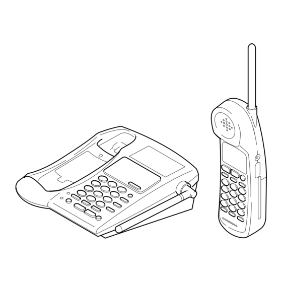
SECTION 1 This section is extracted from instruction manual. GENERAL Identifying the parts Refer to the pages indicated in parentheses for details. Base Phone qj PGM (program) button (p. 34) wd OFF button (p. 27) 1 Display window (p. 24, 34, 52) 9 CHARGE lamp (p. -
Page 4: Setting Up The Base Phone
To L1/L1+L2 You can connect a computer or FAX, etc. to the and/or L2 DATA jack. AC power adaptor DATA jack SPP-IM977 (supplied AC-T128) Notes To the • L2 jack is used for receiving or sending To DATA telephone outlets... -
Page 5: Preparing The Battery Pack
If the battery lasts only a few minutes even after 12 hours of charging, the usable life of the battery has expired and needs replacement. Contact your local Sony authorized dealer or service center, and ask for a Sony BP-T23 rechargeable battery pack. -
Page 6: Making Calls
Step 4: Entering the area code (continued) Select the number (”#1“ to ”#5“) to enter the local area code by turning Jog Dial. Enter three digits of your home area code using the dialing keys. Press Jog Dial. Press (PGM). ”ENTER AREA CODE“... - Page 7 Making calls (continued) Making calls through the speakerphone If the battery becomes weak during a call (MUTING) Press (LINE 1) or (LINE 2) on the base The handset will beep every three seconds five times and E and MUTING (VOLUME) phone.
-
Page 8: Receiving Calls
Receiving calls Note If another call comes in by “call waiting” service while conversing with an When you hear the phone ring, press outside caller, you will hear two short beeps. (LINE 1) or (LINE 2) whichever button is flashing. To inform you of an incoming call, the display shows “** RINGING **”... -
Page 9: Telephone Features
M t N t O t 6 Store a new number, as described previously. Example: to enter “SONY”, press (7) P t Q t R t S t 7 four times (S), press (6) three times T t U t V t 8... - Page 10 ERASE NO YES press Jog Dial. 1234567 • Initial character: To search for “SONY” for example, press (7) and then turn Jog Dial to search through the names starting with P, Q, R, S or 7. Turn Jog Dial up to make “YES” flash, then press Jog Dial.
-
Page 11: Setting The Ringer Type
Setting the ringer type You can select a ringer type of the handset from four type. Turning off the ringer of the handset Perform steps 1 to 5 on page 42. Press (PGM). Press (0). RINGER OFF SELECTED You will hear a confirmation beep. Turn Jog Dial up to make “RINGER”... -
Page 12: Transferring A Call
Talking between the phones (Intercom) (continued) Transferring a call Note You can transfer a call between the handset and base phone without While conversing with an outside caller via the base phone or handset, you disconnecting the call. cannot make an intercom call. If you press (INTERCOM), you will hear a busy tone. -
Page 13: Caller Id Features
Having a conference call (continued) Receiving a call while talking Switching conference from the handset to the base phone If another call comes in while talking, the LINE 1 or LINE 2 button on which another call is coming will flash. Press (HOLD) on the handset to put both lines on hold. -
Page 14: Using The Caller Id List
Looking at the Caller ID list (continued) About the “ *” mark To erase the entire list at once “*” appears if there are more than two calls SMITH JOHN SMITH JOHN Display any Caller ID data. from the same phone number. The older data 1-201-123-4567 1-201-123-4567 will be replaced by the new data, so the calls... - Page 15 Using the Caller ID list (continued) When the local area code matches To change the number of digits of the phone number SMITH JOHN SMITH JOHN 201-123-4567 1-123-4567 If the number of digits of the phone number in the Caller ID list is different from the actual phone number, you need to adjust the number of digits of the phone number to call back or store into the Phone Directory .
- Page 16 Using visual message waiting service (continued) If you move or change your telephone company Message waiting signals are sent in one of two ways: FSK signaling or “stutter” signaling (Your telephone company can provide you with more information about your service). The first time this phone receives a voice mail message, it will set itself to the FSK service and will lock out the stutter service if your telephone company is in FSK service.
-
Page 17: Disassembly
SECTION 2 DISASSEMBLY Note: Follow the disassembly procedure in the numerical order given. CASE (REAR) 6 Remove the case (rear) in the direction of arrow B. 2 two screws (BVTP3 × 12) 1 Remove the “lid (hand), battery case” in the direction of arrow A. 5 claw 4 two claws 3 two claws... - Page 18 BASE (BOTTOM) 2 claw 1 five screws (BTP3 × 12) 3 base (bottom) 2 claw “ringer (SW), knob”, “knob, TP SW” S1001, S1002, S1003 NOTE: On installation BASE MAIN board, adjust to the S1001, S1002 and the S1003. BASE MAIN BOARD, RF UNIT (BASE) 1 three screws BASE MAIN board (BVTP3 ×...
- Page 19 BASE KEY BOARD, SPEAKER (SP1) 1 four screws 2 plate, shield 6 eghit screws 9 KEY board 4 bracket, SPK board 8 contact-C, B/S 5 speaker (SP1), “holder, speaker” 3 Remove two solders of lead. – 19 –...
-
Page 20: Electrical Adjustments
SECTION 3 ELECTRICAL ADJUSTMENTS 2. Adjustment Equipment and Connection BASE UNIT frequency counter 1. Test Mode [Entering the Test Mode] [INTERCOM] While pressing the key, turn the power ON, then – [DIAL MODE] change over the switch. When enter the test mode, [LINE1] [LINE2] [CHARGE]... -
Page 21: Handset
HANDSET 1. Test Mode 2. Adjustment Equipment and Connection [Entering the Test Mode] frequency counter [PGM] 1. Press the key, then displayed “DIRECTORY AREA RINGER” on the LCD. 2. Press the keys, then displayed on – the LCD as below. –... - Page 22 • Frequency Allocation Tables The RF channels for the SPP-IM977 are allocated in fixed pairs as indicated in the tables below. The duplex frequency is maintained at 22.75 MHz for 19 of the 30 channels and 17.95 MHz for the remaining 11 channels.
-
Page 23: Diagrams
SPP-IM977 SECTION 4 DIAGRAMS 4-1. BLOCK DIAGRAM – MAIN Section – CONF, INT COM, SPK2, SPK1, L2, L1 (Page 25) LINE SELECT ANT1 U1001 (1/4) (ANTENNA) TX DATA TX DATA CONF RX AUDIO DSIN LINE AF AMP SELECT U1008 (4/4) -
Page 24: Block Diagram - Display/Key Shift/Power Supply Section
SPP-IM977 4-2. BLOCK DIAGRAM – DISPLAY/KEY SHIFT/POWER SUPPLY Section – Ref No. PANEL DESIGNATION Ref No. PANEL DESIGNATION VOLUME – SPEED DIAL LCD1 VOLUME + TONE P6.0 LCD DB4 LIQUID 0 OPER P6.1 LCD DB5 CRYSTAL 2 ABC DISPLAY 3 DEF... -
Page 25: Block Diagram - Handset Section
SPP-IM977 4-3. BLOCK DIAGRAM – HANDSET Section – ANT2 (ANTENNA) RX PWR B+ RX PWR U1005 RX AUDIO DSIN (SPEAKER) TX PWR B+ BUZZER DRIVE U1002 RINGER Q1009 (BUZZER) TX PWR U1003 TX DATA TXDATA (MIC) RF UNIT B+ SWITCH... -
Page 26: Note For Printed Wiring Boards And Schematic Diagrams
4-4. NOTE FOR PRINTED WIRING BOARDS AND SCHEMATIC DIAGRAMS Note on Printed Wiring Board: Note on Schematic Diagram: • X : parts extracted from the component side. • All capacitors are in µF unless otherwise noted. pF: µµF • Y : parts extracted from the conductor side. 50 WV or less are not indicated except for electrolytics •... - Page 27 SPP-IM977 • Waveforms – BASE MAIN Board – – HAND MAIN Board – 1 U1014 qa (XOUT) 3 U1001 rl (XTAL1) IV/DIV, 100 ns/DIV 400 mV/DIV, 20 ns/DIV 820 mVp-p 2.8 Vp-p 279 ns 54.3 ns 2 U1000 rl (XTAL1)
-
Page 28: Printed Wiring Board - Base Main Board (Component Side)
SPP-IM977 4-5. PRINTED WIRING BOARD – BASE MAIN Board (Component Side) – • Semiconductor Location BASE MAIN BOARD (COMPONENT SIDE) Ref. No. Location D1010 D1000 I-10 C1056 D1002 D1003 H-11 R1171 D1007 Q1008 Q1009 R1180 R1153 R1165 D1008 H-10 R1181... -
Page 29: Printed Wiring Board - Base Main Board (Conductor Side)
SPP-IM977 4-6. PRINTED WIRING BOARD – BASE MAIN Board (Conductor Side) – • Semiconductor Location BASE MAIN BOARD (CONDUCTOR SIDE) Ref. No. Location J1008 D1004 DATA D1005 D1006 D1011 J1018 D1014 T1000 D1016 LINE TRANSFORMER D1017 D1021 C1084 D1018 D1017... -
Page 30: Schematic Diagram – Base Main Board (1/3)
SPP-IM977 4-7. SCHEMATIC DIAGRAM – BASE MAIN Board (1/3) – • See page 47 for IC Block Diagram. (Page 39) (Page 37) – 35 – – 36 –... -
Page 31: Schematic Diagram – Base Main Board (2/3)
SPP-IM977 4-8. SCHEMATIC DIAGRAM – BASE MAIN Board (2/3) – • See page 30 for Waveform. • See page 47 for IC Block Diagrams. (Page 39) (Page 36) – 37 – – 38 –... -
Page 32: Schematic Diagram – Base Main Board (3/3)
SPP-IM977 4-9. SCHEMATIC DIAGRAM – BASE MAIN Board (3/3) – • See page 30 for Waveform. • See page 48 for IC Block Diagram. (Page 36) (Page 38) (Page 42) – 39 – – 40 –... -
Page 33: Printed Wiring Board - Base Key Board
SPP-IM977 4-10. PRINTED WIRING BOARD – BASE KEY Board – 4-11. SCHEMATIC DIAGRAM – BASE KEY Board – • Semiconductor Location LCD1 Ref. No. Location LIQUID CRYSTAL DISPLAY BASE KEY BOARD D4, 15-19 (LCD BACK LIGHT) D4, 6, 13, 15-19... -
Page 34: Printed Wiring Board - Hand Main Board
SPP-IM977 4-12. PRINTED WIRING BOARD – HAND MAIN Board – • Semiconductor Location Ref. No. Location HAND MAIN BOARD (COMPONENT SIDE) D1001 D-12 D1002 B-12 D1003 E-11 D1004 D-12 C1055 D1006 C-12 U1005 R1079 C1021 3 2 1 C1048 D1020 –... -
Page 35: Schematic Diagram - Hand Main Board
SPP-IM977 4-13. SCHEMATIC DIAGRAM – HAND MAIN Board – • See page 30 for Waveform. • See page 49 for IC Block Diagram. – 45 – – 46 –... - Page 36 SPP-IM977 • IC Block Diagrams – BASE MAIN Board – U1013 U4083B U1002, 1028 MC74HC4053DTR2 15 14 BIAS CIRCUIT U1012, 1020, 1021 SN74HC595ADB-E05 SHIFT REGISTER LATCH PARALLEL DATA OUTPUT – 47 –...
- Page 37 U1014 PCC317 U1015 ILC7081AIM5-30 TRANS- ERROR ALERT SIGNAL CONDUCTANCE BANDGAP HIGH TONE REFERENCE – IN– VOUT FILTER VREF TONE ST/GT DETECTION ALGORITHM ALERT SIGNAL INTERNAL LOW TONE ANTI-ALIAS FILTER GUARD CNOISE FILTER ON/OFF TIME BIAS VREF GENERATOR INTERRUPT GENERATOR CARRIER TRIGIN DETECTOR TRIGRC...
- Page 38 U1019 U4082B VREF ATTEN- DIAL UATOR TONE DETECTOR BACKGROUND BACKGROUND LEVEL LEVEL NOISE NOISE DETECTOR DETECTOR DETECTOR DETECTOR COMPARATOR COMPARATOR LEVEL LEVEL DETECTOR DETECTOR HYBRID HYBRID ATTENUATOR AMP 2 AMP 1 FILTER – – – – HAND MAIN Board – U1007 LP29811M5-3.0 OVER CURRENT/ OVER TEMP...
-
Page 39: Exploded Views
SECTION 5 EXPLODED VIEWS NOTE: • -XX and -X mean standardized parts, so they • Items marked “*” are not stocked since they may have some difference from the original are seldom required for routine service. Some one. delay should be anticipated when ordering •... - Page 40 (2) BASE SET SECTION LCD1 ANT1 (Including A) supplied not supplied supplied supplied Ref. No. Part No. Description Remark Ref. No. Part No. Description Remark 3-041-534-01 FOOT, RUBBER 4-356-741-11 SCREW TAPPING (BIND 2X6) 3-039-938-01 BASE (BOTTOM) 3-041-536-01 SHEET 3-041-523-01 RINGER (SW), KNOB 3-041-552-01 HOLDER (BU975), LCD 3-038-077-01 KNOB, TP SW 3-041-274-01 HOLDER, SPEAKER...
-
Page 41: Electrical Parts List
BASE KEY SECTION 6 BASE MAIN ELECTRICAL PARTS LIST NOTE: • Due to standardization, replacements in the • Items marked “*” are not stocked since they The components identified by mark 0 or dotted line with mark parts list may be different from the parts speci- are seldom required for routine service. - Page 42 BASE MAIN Ref. No. Part No. Description Remark Ref. No. Part No. Description Remark C1051 1-104-847-11 TANTALUM CHIP 22uF C1119 1-107-826-11 CERAMIC CHIP 0.1uF C1052 1-107-826-11 CERAMIC CHIP 0.1uF C1120 1-162-907-11 CERAMIC CHIP 0.25PF 50V C1121 1-162-917-11 CERAMIC CHIP 15PF C1053 1-107-826-11 CERAMIC CHIP 0.1uF...
- Page 43 BASE MAIN Ref. No. Part No. Description Remark Ref. No. Part No. Description Remark D1007 8-719-909-90 DIODE BAV99 R1020 1-216-836-11 METAL CHIP 1/16W D1008 8-719-909-90 DIODE BAV99 R1022 1-216-813-11 METAL CHIP 1/16W D1010 8-719-047-37 DIODE BAS16 D1011 1-801-730-11 VARISTOR R1023 1-216-813-11 METAL CHIP 1/16W R1024...
- Page 44 BASE MAIN Ref. No. Part No. Description Remark Ref. No. Part No. Description Remark R1082 1-216-833-11 RES, CHIP 1/16W R1151 1-218-345-11 RES, CHIP 9.1K 1/16W R1083 1-216-789-11 METAL CHIP 1/16W R1152 1-216-222-00 RES, CHIP 1/8W R1085 1-216-838-11 METAL CHIP 1/16W R1153 1-216-222-00 RES, CHIP 1/8W...
- Page 45 BASE MAIN HAND MAIN Ref. No. Part No. Description Remark Ref. No. Part No. Description Remark < SWITCH > C1012 1-110-501-11 CERAMIC CHIP 0.33uF C1013 1-135-181-21 TANTALUM CHIP 4.7uF 6.3V S1001 1-771-833-11 SWITCH, SLIDE (L2 RINGER LEVEL) S1002 1-771-833-11 SWITCH, SLIDE (L1 RINGER LEVEL) C1014 1-163-038-00 CERAMIC CHIP 0.1uF...
- Page 46 HAND MAIN Ref. No. Part No. Description Remark Ref. No. Part No. Description Remark D1027 8-719-063-83 LED SML-510MWT86 (LCD BACK LIGHT) R1068 1-216-821-11 METAL CHIP 1/16W D1028 8-719-063-83 LED SML-510MWT86 (LCD BACK LIGHT) R1073 1-216-802-11 RES, CHIP 1/16W D1030 8-719-069-29 DIODE RB520S-30TE61 R1079 1-216-789-11 METAL CHIP 1/16W...
- Page 47 SPP-IM977 Ref. No. Part No. Description Remark Ref. No. Part No. Description Remark U1005 1-505-593-11 SPEAKER (2.8cm) ************************************************************ ************** HARDWARE LIST ************** 7-685-534-19 SCREW +BTP 2.6X8 TYPE2 N-S 7-685-548-19 SCREW +BTP 3X12 TYPE2 N-S 7-685-648-79 SCREW +BVTP 3X12 TYPE2 IT-3 ************************************************************ ACCESSORIES &...
Need help?
Do you have a question about the SPP-IM977 and is the answer not in the manual?
Questions and answers