
Subscribe to Our Youtube Channel
Related Manuals for Stanford Research Systems CG635


Summary of Contents for Stanford Research Systems CG635
- Page 1 Distribution in the UK & Ireland User Manual www.lambdaphoto.co.uk CG635 2.05 GHz Synthesized Clock Generator Revision 1.3 (08/2010)
- Page 2 (1) year from the date of shipment. Service For warranty service or repair, this product must be returned to a Stanford Research Systems authorized service facility. Contact Stanford Research Systems or an authorized representative before returning this product for repair.
-
Page 3: Table Of Contents
Changing a Parameter Stepping a Parameter Step Sizes of Exact Factors of Ten Changing Units Store and Recall Settings Secondary Functions Q and Q ¯ Outputs CMOS Output Frequency Phase Secondary Functions RUN, STOP, TOGGLE INIT CG635 Synthesized Clock Generator... - Page 4 Instrument Status Register PLL Lock Status Register Error Codes Performance Evaluation Overview Equipment Required CG635 Self Test Output Level Tests Q/Q ¯ Level Tests CMOS Level Tests Transition Time Measurements Frequency Synthesis Tests Functional Tests Time Modulation Test CG635 Synthesized Clock Generator...
- Page 5 Rear-Panel RJ-45 Outputs RS-232 and GPIB Interfaces Power Supply Interface Front-Panel Output Drivers Front-Panel Q and Q ¯ Drivers Front-Panel CMOS Driver Front-Panel Display and Keypad Power Supply Timebase Options Optional PRBS Generator Line Receiver Accessories CG635 Synthesized Clock Generator...
- Page 6 Contents Parts List Motherboard Assembly Output Driver Assembly Power Supply Assembly Chassis and Front-Panel Assembly Option 1 Assembly Option 2 Assembly Option 3 Assembly Schematics CG635 Schematic Diagram List CG635 Synthesized Clock Generator...
-
Page 7: Safety And Preparation For Use
Safety and Preparation for Use Line Voltage The CG635 operates from a 90 to 132 VAC or 175 to 264 VAC power source having a line frequency between 47 and 63 Hz. Power consumption is less than 80 VA total. In standby mode, power is turned off to the main board. - Page 8 Symbols you may Find on SRS Products Symbol Description Alternating current Caution - risk of electric shock Frame or chassis terminal Caution - refer to accompanying documents Earth (ground) terminal Battery Fuse On (supply) Off (supply) CG635 Synthesized Clock Generator...
-
Page 9: Specifications
<1 ps (1 kHz to 5 MHz bandwidth) Wander (p-p) <20 ps (10 s persistence) Time Modulation Rear-panel input BNC, DC coupled, 1 k Sensitivity 1 ns/V, ±5 % Range ±5 ns Bandwidth DC to greater than 10 kHz CG635 Synthesized Clock Generator... - Page 10 7 and pin 8 Load impedances between pin 7 and pin 8 Logic levels = +0.9 V, V = +2.2 V HIGH Recommended cable Straight-through Category-6 Protection Continuous to ground, momentary to +5 V CG635 Synthesized Clock Generator...
- Page 11 <30 W (std. timebase) <40 W (opt. 02, OCXO timebase) <50 W (opt. 03, Rb timebase) Dimensions 8.5” × 3.5” × 13” (WHD) Weight <9 lbs. Warranty One year parts and labor on defects in materials and workmanship CG635 Synthesized Clock Generator...
- Page 12 Specifications Optional Receiver Modules General Inputs RJ-45. Connects to CG635 via standard Category-6 cable. Outputs Q / Q ¯ on SMA connectors Dimensions 1 5/8” × 1” × 3” (WHD) Models Model Levels Source Termination Transition Impedance Impedance Time (max)
-
Page 13: Quick Start Instructions
1. With the power button in the Standby position, connect the CG635 to a grounded outlet using the power cord provided. 2. Push in the power button to turn on the CG635. The CG635 will perform some start up tests and then recall the instruments’ last known settings from non volatile memory. - Page 14 15. For more details about the operation of keys on the front panel, see the Front Panel Overview (page 2) in the Introduction. 16. For more details about a particular feature, see the chapter Operation (page 13). CG635 Synthesized Clock Generator...
-
Page 15: Introduction
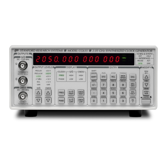
The CG635 generates single ended and differential clocks from 1 µHz to 2.05 GHz with sub-picosecond jitter. Clock frequencies may be set with up to 1 pHz resolution and 16 significant digits. -
Page 16: Front-Panel Overview
The front panel was designed to provide a simple, intuitive, user interface to all the CG635 features (see Figure 1). The power switch is located in the lower right corner of the front panel. Pushing the switch enables power to the instrument. Pushing the switch again places the instrument in stand-by mode, where power is enabled only to optionally installed timebases. -
Page 17: Output Levels
Output Levels Standard Levels The CG635 provides a simple method for switching among five standard voltage levels for the Q / Q ¯ and CMOS outputs. The meaning of the five standard levels is summarized in Table 1 and Table 2 below: Table 1: Q / Q ¯... -
Page 18: Display
Entry Numeric Entry The ENTRY section is used to modify the current settings of the CG635. In most cases, the currently displayed item can be changed by entering a new value with the numeric keys, and pressing an appropriate units key to complete the entry. For example, if the frequency is currently being displayed, pressing the keys ‘1’, ‘MHz’, sequentially will... - Page 19 Increments the phase by 90 degrees and displays phase GPIB Enables the GPIB remote interface. Disables RS-232. ADDRS Displays / Sets the GPIB primary address for the CG635 RS-232 Enables the RS-232 remote interface. Disables GPIB. DATA Displays the most recent data received over the remote interface Increases the current step size by the next exact factor of ten (Located in the MODIFY section.)
-
Page 20: Modify
1 Hz to 123457.789 Hz. Remote and Local Mode The REM LED turns on when the CG635 is placed in remote mode by the GPIB bus. In this mode, all the front panel keys are disabled and the instrument can only be controlled via the GPIB bus. -
Page 21: Clock Status And Interface Indicators
10 MHz & SYNTH. This contains the EXT and UNLK LEDs. The EXT LED indicates that the CG635 has detected an external 10 MHz reference at the 10 MHz input BNC on the rear panel of the CG635. The CG635 will lock its internal clock to this external reference. -
Page 22: Rear-Panel Overview
Figure 2: The CG635 Rear Panel AC Power The Power Entry Module is used to connect the CG635 to a power source through the power cord provided with the instrument. The center pin is connected to the CG635 chassis so that the entire box is grounded. -
Page 23: Chassis Ground
1 k impedance. The CG635 will automatically detect the presence of an external 10 MHz reference and lock to it if possible. If the CG635 is unable to lock to the external reference, the front-panel UNLK LED will turn on and stay on until the CG635 either successfully locks to the external reference or the reference is removed. -
Page 24: Clock Output
The CG635 interfaces to a number of optional clock receiver modules which can be used to get a clock signal from the CG635 to where it is needed. The receiver modules regenerate the clock locally providing the user with clean, fast clock edges, even if the CG635 is several meters away. -
Page 25: Prbs And Clock Option
The most common way to create a PRBS generator is to use a linear shift-register, feeding the input of the shift-register with the exclusive OR of two (particular) data bits as they shift through the system. The CG635 uses a 7-bit ECL shift register that provides a pseudo-random bit sequence which repeats after 2 –... -
Page 27: Operation
Power On At power on, the CG635 performs a number of self tests to verify that various internal components are operating correctly. If any of the tests fail, the CG635 will briefly display “Failed”... -
Page 28: Changing A Parameter
MODIFY keys, respectively. For example, if the current frequency step size is being displayed as 1.000 Hz, then pressing MODIFY will increase to the step size to 10.000 Hz. CG635 Synthesized Clock Generator... -
Page 29: Changing Units
Frequency has the option of being displayed in units of GHz, MHz, kHz, or Hz. When the user enters a frequency using the front panel, the CG635 will display the frequency in the units used to complete the entry. For example, pressing the keys ‘FREQ’, ‘1’, ‘0’, ‘kHz’... -
Page 30: Q And Q ¯ Outputs
10 k series) and –1.020 V (for the 100 k series), while V is –1.745 V (for the 10 k series) and –1.820 V (for the 100 k series). As seen in Table 7, the CG635 will provide a of –1.00 V and a V of –1.80 V. -
Page 31: Cmos Output
5.5 V exceeds the upper limit for V . On the other hand, setting V HIGH HIGH 5.0 V will cause the CG635 to briefly display “Lo is 4.00” and to set V and V HIGH 5.00 V and 4.00 V, respectively. V... - Page 32 OUTPUT LEVELS section of the front panel. When the CMOS output is at a standard level, the CG635 will highlight the appropriate standard level LED. The meaning of the five standard levels is summarized in the Table 9.
-
Page 33: Frequency
Frequency The CG635 can output frequencies in the range 1 µHz to 2.05 GHz with up to 1 pHz of resolution and 16 significant digits. The frequency may be set to arbitrary values, or stepped up and down by configurable step sizes by following the instructions described in the Front-Panel User Interface section at the beginning of this chapter. -
Page 34: Phase
FREQ/2 and FREQx2. Phase The CG635 can adjust the phase of the output by up to 360° per step. The phase may be set to arbitrary values, or stepped up and down by configurable step sizes by following the instructions described in the Front-Panel User Interface section at the beginning of this chapter. - Page 35 1 µHz ” f ” 2 Hz 0.000000001° If the user tries to enter a phase with more resolution than permitted, the CG635 will truncate the result to the appropriate resolution. When the user changes frequency, the CG635 will automatically reset the phase to 0°, and truncate the phase step size to the resolution allowed at the new frequency.
-
Page 36: Secondary Functions
STATUS The STATUS function displays a number of instrument parameters which characterize the current status of the CG635. The user can cycle through each of the parameters by pressing the MODIFY keys. The meaning of each of the parameters is summarized in Table 13. - Page 37 The STATUS parameter displays the current value of the CG635 serial poll status byte. This is the same value that is returned by the *STB? command. See the CG635 Remote Programming chapter for information on how to interpret the status byte.
-
Page 38: Prbs On/Off
PRBS ON/OFF If the PRBS option is installed, the PRBS ON function enables the PRBS output, and the PRBS OFF disables it. The CG635 will briefly display ‘PRBS on’ or ‘PRBS off’, respectively, when the functions are accessed. If the PRBS option is not installed, the CG635 will briefly display ‘no PRBS.’... -
Page 39: Addrs
Factory Default Settings The factory default settings are listed in Table 15. The CG635 may be forced to assume its factor default settings by power cycling the unit with the ‘BACK SPACE’ key depressed. The INIT secondary function and the *RST remote command reset all but the communication parameters back to factory default settings. -
Page 40: Troubleshooting
Power-on Status Clear (*PSC) Troubleshooting The CG635 does not include any user serviceable parts inside. The line fuse is internal to the instrument and may not be serviced by the user. In the event of instrument failure, refer service to a qualified technician. - Page 41 PC, make sure you are using a standard PC serial cable, not a “null-modem” cable. Doesn’t respond to key presses The CG635 has been placed in remote mode by the and REM LED is on GPIB bus. Press ‘STEP SIZE’ to put the CG635 back into local mode.
-
Page 43: Cg635 Remote Programming
INTERFACE section: RS-232, GPIB, ACT, and ERR. The RS-232 LED is on when the CG635 is configured to accept commands over RS-232. The GPIB LED is on when the CG635 is configured to accept commands over GPIB. The ACT LED serves as an activity indicator that flashes every time a character is received or transmitted over one of the remote interfaces. -
Page 44: Command Syntax
Communications with the CG635 is done with ASCII characters. All commands are 4-characters long and are case-insensitive. Standard IEEE-488.2 defined commands begin with the ‘*’ character followed by three letters. CG635 specific commands are composed of four letters. The four-letter mnemonic (shown in CAPS) in each command sequence specifies the command. -
Page 45: Index Of Commands
Page 39 Communication Error Status Register INSE(?){i} Page 39 Instrument Status Enable INSR? Page 39 Instrument Status Register LCKE(?){i} Page 39 PLL Lock Status Enable LCKR? Page 39 PLL Lock Status Register LERR? Page 39 Last Error CG635 Synthesized Clock Generator... -
Page 46: Instrument Control Commands
Set (query) the PRBS enabled state {to i}. If i is 0, PRBS is disabled. If i is 1, PRBS is enabled. QOUT(?) i,{j} Q / Q ¯ Output Set (query) the i component of the Q / Q ¯ output {to j}. The parameter i selects the Q / Q ¯ component. CG635 Synthesized Clock Generator... - Page 47 PECL 3.3 V levels (2.30/1.50 V) PECL 5.0 V levels (4.00/3.20 V) The query form returns 1 if the current levels do not correspond to one of the standard levels. This indicates that the VAR LED is on. CG635 Synthesized Clock Generator...
- Page 48 Step Q / Q ¯ high Step Q / Q ¯ low Step CMOS high Step CMOS low TIMB? Timebase Query the current timebase for the CG635. The returned value identifies the timebase. Value Meaning Internal timebase OCXO timebase Rubidium timebase...
- Page 49 CG635 Remote Programming The parameter i selects the item. Display Item Frequency Frequency Step The parameter j selects the units. Display CG635 Synthesized Clock Generator...
-
Page 50: Interface Commands
This location is automatically updated ten seconds after the user presses any key that modifies the current state of the instrument. The following settings are saved: 1. Current frequency and frequency step size. 2. Current phase and phase step size. CG635 Synthesized Clock Generator... - Page 51 Run the instrument self test and return the result. *WAI Wait for Command Execution The instrument will not process further commands until all prior commands including this one have completed. Example *WAI<CR> Wait for all prior commands to execute before continuing. CG635 Synthesized Clock Generator...
-
Page 52: Status Reporting Commands
*SRE(?){i} Service Request Enable Set (query) the Service Request Enable register {to i}. Bits set in this register cause the CG635 to generate a service request when the corresponding bit is set in the serial poll status register. *STB? Serial Poll Status Byte Query the standard IEEE 488.2 serial poll status byte. - Page 53 LERR?. The error buffer has space to store up to 20 errors. If more than 19 errors occur without being queried, the 20 error will be 254 (Too Many Errors) indicating that errors were dropped. CG635 Synthesized Clock Generator...
-
Page 54: Status Byte Definitions
CG635 Remote Programming Status Byte Definitions The CG635 reports on its status by means of the serial poll status byte and four event status registers: the standard event status (*ESR), the communication error status (CESR), the PLL lock status (LCKR), and the instrument event status (INSR). These read-only registers record the occurrence of defined events inside the CG635. -
Page 55: Standard Event Status Register
Overrun error. An RS-232 character was received before the CG635 had time to process the previous character. OVFL The input buffer of the CG635 overflowed. The CG635 was addressed to talk under GPIB, but there were no listeners. Reserved DCAS Device clear active state. -
Page 56: Pll Lock Status Register
The PLL lock status register may be queried with the LCKR? command. The PLL status enable register (LCKE) may be used to control the setting of the LCKB summary bit in the serial poll status byte. CG635 Synthesized Clock Generator... -
Page 57: Error Codes
CG635 Remote Programming Error Codes The CG635 contains an error buffer that may store up to 20 error codes associated with errors encountered during power-on self tests, command parsing, or command execution. The errors in the buffer may be read one by one by executing successive LERR? commands. The meaning of each of the error codes is described below. - Page 58 No Listener This is a communications error that occurs if the CG635 is addressed to talk on the GPIB bus, but there are no listeners. The CG635 discards any pending output.
- Page 59 The ROM checksum failed. The firmware code is likely corrupted. Failed 24 V Out of Range The CG635 24 V power is out of range. Failed 19.44 MHz Low Rail The 19.44 MHz crystal can not tune to low enough frequencies.
- Page 60 Failed Optional Timebase An installed optional timebase is not oscillating. Failed Clock Symmetry The clock output symmetry is out of specification Other Errors Too Many Errors The error buffer is full. Subsequent errors have been dropped. CG635 Synthesized Clock Generator...
-
Page 61: Performance Evaluation
Performance Evaluation Overview The performance of a CG635 may be evaluated by running a series of tests designed to measure the accuracy of its inputs and outputs and comparing the results with their associated specifications. While the performance tests presented here are not as extensive as the tests performed at the factory, one can nevertheless have confidence that a unit that passes these tests is functioning properly and within specification. -
Page 62: Output Level Tests
CG635 over a remote interface. Output Level Tests The output level tests are intended to test the accuracy and integrity of the CG635 output drivers. They test the accuracy of the DC voltage levels at each of the supported communication standards. -
Page 63: Cmos Level Tests
(3.158, 3.950) (3.242, 4.050) To test the Q ¯ output, configure the CG635 as in Figure 4, except swap the connections to Q and Q ¯ . Repeat the steps above except record V in step 4 and record V in step 6. -
Page 64: Transition Time Measurements
(–0.120, 4.880) (0.120, 5.120) Transition Time Measurements The 20 % to 80 % output transition times of the CG635 are tested using the HP 54120A Digitizing Oscilloscope with HP 54121A four channel input module. Configure the setup as in Figure 6. - Page 65 Table 22: Maximum allowed transition times for Q/Q ¯ outputs Output Meas. (Rising, Falling) ps Max. ( Rising, Falling) ps (100, 100) Q ¯ (100, 100) CMOS Timing Measurements For the CMOS output timing measurements, configure the HP 54120A digitizing scope as in Table 23. CG635 Synthesized Clock Generator...
-
Page 66: Frequency Synthesis Tests
DC to 2 GHz. This ensures that all the dividers are working properly. Overall stability of the CG635 is tested by measuring the phase noise, jitter, and wander at a couple of specific frequencies. The test points ensure that both crystals used in the frequency generation are operating at specification. -
Page 67: Functional Tests
Figure 7: Setup for frequency measurements from 1.0 to 2.0 GHz. The SR625 prescaler has a level adjustment knob. Adjust the level until the SR620 reports frequencies that are 1/10 of the set frequency. Set the frequency of the CG635 to CG635 Synthesized Clock Generator... - Page 68 50 Ω terminator Figure 8: Setup for frequency measurements below 1.0 GHz. Set the frequency of the CG635 to each value given in Table 26. Record the frequency measured by the SR620. Verify that the measured frequency is within the limits specified in Table 26.
-
Page 69: Time Modulation Test
SR620 configuration except make sure the channel A UHF prescaler is not activated. Set the frequency of the CG635 to each value given in Table 27. Record the frequency measured by the SR620. Verify that the measured frequency is within the limits specified in Table 27. -
Page 70: Phase Noise Tests
Use the setup shown in Figure 10 to measure phase noise and jitter. Note that since the CG635 is locked to the FS725, this setup will test the noise of the synthesizer alone, independent of the internal timebase. - Page 71 Phase Noise Test Procedure At each test point identified in Table 30, set the CG635 to the given frequency. Then set the HP 89440A to the given center frequency, span, and marker position. Record S(f) reported by the HP 89440A at the marker position in units of dBradrms /Hz.
-
Page 72: Jitter Tests
1 kHz to 5 MHz. The HP 89440A does not have adequate bandwidth to measure out to 5 MHz. However, the spectrum of the noise from the CG635 is flat from 1 MHz to 5 MHz. Therefore, the jitter can be approximated by assuming that the rms noise in the band from 1 MHz to 5 MHz is equal to 2 times the measured rms noise in the band from 1 MHz to 2 MHz. -
Page 73: Timebase Calibration
The accuracy of the internal timebase may be tested against a house reference if it is known that the house reference has a superior stability and accuracy than the timebase installed in the CG635. Use the setup shown in Figure 11 to test the accuracy of the timebase. -
Page 74: Timebase Calibration Test
10. Press the GATE/ARM button once to set the gate to 10 s 11. If a rubidium timebase is installed in the CG635, press the GATE/ARM button once more to set the gate to 100 s 12. Press the SAMPLE SIZE button three times to set the sample size to 1. -
Page 75: Circuit Description
Resolution The frequency resolution of the CG635 is determined by the frequency resolution of the DDS frequency synthesizer used in the system. The CG635 uses a 48-bit DDS; however the frequency resolution is extended to 64 bits by frequency-shift keying (FSK) the least significant bit (LSB) of the DDS with a duty factor with 16 bits of resolution. -
Page 76: Circuit Block Diagram
While the in-close phase noise of this reference is very good, there is a thick forest of spurious components in the broadband spectrum below –80 dBc. These spurs must be eliminated in order for the frequency reference to be useful for synthesizing an RF output. CG635 Synthesized Clock Generator... -
Page 77: Reference Synthesizer Clean-Up
A low pass filter (with a bandwidth that is decreased as the R divider is increased) filters the dual modulus synthesizer’s phase detector output. The output of the filter controls the VCO which can operate over the range of 960-2050 MHz. CG635 Synthesized Clock Generator... -
Page 78: Programmable Dividers And Clock Fan-Out
0.000,001,705,302 0.000,003,637,978 0.000,000,852,651 0.000,001,818,989 For frequencies in bands eleven to fifty, the CG635 uses DDS technology to seamlessly change dividers. Since no spurious pulses are generated, the output is not disabled. Determining Register Values Definitions = 20 MHz timebase reference (which can be locked to an external 10 MHz) = DDS synthesizer output frequency (±100 ppm of 19.40 MHz or 19.44 MHz) - Page 79 Test if the computed f satisfies the condition f VCXO VCXO f. If the test fails, increment R and go to (b.) g. Parse N into A & B registers: B = INT(N/8) & A = N - 8×B CG635 Synthesized Clock Generator...
- Page 80 2084 19.48051948 2084 19.48051948 2084 19.41747573 –1159 19.43005181 –512 19.43844492 –80 5. The first table shows that R=16 and N=1237 allows us to generate 750 MHz with the VCXO running 92 ppm above its nominal value. CG635 Synthesized Clock Generator...
-
Page 81: Phase Adjustment
–159+60 = –99 dBc/Hz. Phase adjustment The CG635 allows the phase of the output to be viewed and adjusted from the front panel or via the computer interface. Since the output edges are phase locked to the internal DDS edges, output edges will move by the same amount of time as the DDS edges. - Page 82 = 1.06666 µs / 262,114 µs = 4.069476 ppm So we see that t is long enough to avoid having the VCXO come unlocked ( f § 4 ppm), but not so long as to cause the user to grow impatient with the phase CG635 Synthesized Clock Generator...
-
Page 83: Detailed Circuit Description
0.1 µF capacitor. Timebase Main Board, Schematic sheet “CG_MB1D” The frequency reference for the CG635 Synthesized Clock Generator is a 20 MHz Colpitts oscillator. The oscillator’s resonator (Y100) is a 3 overtone AT-cut crystal designed to operate at 20 MHz with a 20 pF load. The load capacitance is the series combination of D100 (a dual varactor), C121 and C122 in parallel with L103. - Page 84 Minimum pulse widths will be seen at the Q outputs of U106A/B when the PLL circuit achieves phase-lock. The pulse widths will be equal to the sum of the propagation delays through the OR gate (U107, 0.9-3.6 ns) and the flip-flops (U106, 1.0-5.4 ns). Meta- CG635 Synthesized Clock Generator...
-
Page 85: Dds And The 19.40/19.44 Mhz Reference
DDS and the 19.40/19.44 MHz Reference Main Board, Schematic sheet “CG_MB2D” Clock outputs from the CG635 are generated by dividing down the output of an RF synthesizer. The RF synthesizer operates between 950 MHz and 2050 MHz and is used without division to provide clock outputs in that range. - Page 86 R218/C248), and an integrating loop filter (U204A and surrounding R’s and C’s). The phase/frequency detector compares the phase of the DDS to the phase of the selected VCXO. If the DDS leads in phase, then the output of the phase/frequency detector will CG635 Synthesized Clock Generator...
-
Page 87: Time Modulation
Time Modulation Main Board, Schematic sheet “CG_MB3D” The CG635 has a rear panel time-modulation input (J300) which allows an analog voltage to modulate the timing of the clock outputs. This input is calibrated to have a sensitivity of 1 ns/V and a full-scale range of ±5 ns. The input is DC coupled and so may be used as a DC phase adjustment of the clock outputs. -
Page 88: Rf Synthesizer
(1) Vhigh = +2.34 V, (2) Vlow = +1.55 V, (3) t = 175 ps, (4) t = 140 rise fall ps, (5) t < 1 ps , (6) f = 960 MHz, and (7) f = 2050 MHz. jitter CG635 Synthesized Clock Generator... -
Page 89: Ecl Dividers And Clock Multiplexer
U408, a programmable divider that has programmable phase jumps. An ECL 1:4 multiplexer (U404) is used to select one of four sources for output from the CG635: (1) the undivided “top octave” clock, (2) the “top octave” clock divided by 2 by U400, (3) the top octave clock divided by 4 ×... -
Page 90: Microcontroller
10MHZ_LEAD is a voltage proportional to the amount by which the external reference or optional reference leads the 20 MHz timebase. The front- panel UNLOCK LED will be lit if the instrument is trying to lock the 20 MHz timebase CG635 Synthesized Clock Generator... - Page 91 PECL clock source. The signal is useful for measuring the duty cycle of the top octave clock signal when compared to +CLK_TST. The analog DAC voltage CAL_SYM will be adjusted to equalize +CLK_TST and –CLK_TST to assure 50/50 duty cycle in the top octave. CG635 Synthesized Clock Generator...
- Page 92 KEY0-KEY4: Five key strobe lines. One of the five lines will go “high” when a front panel key is pressed during the column strobe period for that key. All five inputs have their active pull-downs enabled. -DONE: This line goes low when the phase jump requested of U408 has been completed. CG635 Synthesized Clock Generator...
- Page 93 FSK_DDS: Pulse width modulated signal whose duty cycle is controlled with 16 bits of resolution to extend the resolution of the 48-bit DDS to 64 bits. SDO: Synchronous serial data output for data transfer to octal DAC and dual-modulus synthesizer. CG635 Synthesized Clock Generator...
- Page 94 CAL_SYM will decrease +CLK_TST and increase –CLK_TST. The required value may be a function of frequency. Q_AMPL: Controls the amplitude of the front panel Q & -Q outputs. The output § 0.276 × Q_AMPL. amplitude, Q , is given by: Q AMPL AMPL CG635 Synthesized Clock Generator...
- Page 95 U507 (even digit segments), and U509 (LED lamps.) Writing a “0” will turn “on” the corresponding segment or lamp, writing a “1” will turn it “off”. 3. A single “1” is written to U508 to enable a single strobe line. CG635 Synthesized Clock Generator...
-
Page 96: Rear-Panel Rj-45 Outputs
MOSFET is turned “off” by U611A if the current seen in the shunt resistors (R617, R618 & R641) exceeds 375 mA. A co-packaged Schottky diode in U612 prevents the +5 VDC from being pulled below ground. CG635 Synthesized Clock Generator... -
Page 97: Rs-232 And Gpib Interfaces
Power Supply Interface Main Board, Schematic sheet “CG_MB6D” The CG635 uses a universal input switching power supply in a separate enclosure to power the system. The power supply has a +24 V output which is “on” whenever the instrument has line voltage (whether or not the power switch is “on”). This power supply powers the optional timebase (an OCXO or rubidium) even while the instrument is “off”. -
Page 98: Front-Panel Q And Q ¯ Drivers
The baseline for the output, which is normally at 0 VDC, may be offset by ±1.00 VDC. This output is normally not terminated with 50 . Doing so will not damage the output, and will improve the CG635 Synthesized Clock Generator... -
Page 99: Front-Panel Display And Keypad
Power Supply Schematic sheet “CG_PS1B” The modular power supply for the CG635 is in a separate shielded case inside the instrument. The power supply consists of universal input, 60 W, +24 V, OEM switching power supply which is “on” whenever power is applied to the unit (whether or not the power switch is in the “on”... -
Page 100: Timebase Options
The most common way to create a PRBS generator is to use a linear shift-register, feeding the input of the shift-register with the exclusive-or of two (particular) data bits as they shift through the system. The CG635 uses a 7-bit ECL shift register that provides a CG635 Synthesized Clock Generator... -
Page 101: Line Receiver Accessories
UTP cable. Line Receiver Accessories The rear-panel of the CG635 has an RJ-45 connector to provide clock signals at RS-485 and LVDS levels as well as ±5 VDC. A series of line receiver accessories are used to receive the clock signals over an unshielded, four-pair, CAT-6 cable and convert the clock to single-ended complementary logic outputs on SMA connectors. - Page 102 “1” outputs, allowing for a high return loss for both levels.Terminating the outputs will not damage the module, but doing so will reduce the amplitude of the outputs by a factor of 2×. CG641 and CG642 line receivers Schematic sheet “CG_LR2B” CG635 Synthesized Clock Generator...
- Page 103 The magnitude of the current switched by U304 is controlled by R308. Both SMA outputs should be terminated with 50 loads. (Except for the CG643, which provides +5 V PECL level outputs into unterminated 50 cables.) CG635 Synthesized Clock Generator...
- Page 104 “fault” conditions. The transistor Q500 imitates a laser diode’s photo monitor by providing small current that increases with the MAX3737’s bias current generator. U504 provides a reset to U503 in the case that a CG635 Synthesized Clock Generator...
- Page 105 The SMA outputs are intended to drive 50 loads to ground. Both outputs should be terminated. (Without a terminator, the open emitter outputs of U202 will be biased “off”, and there will be no clock at the SMA output.) CG635 Synthesized Clock Generator...
-
Page 107: Parts List
Cap, Ceramic 50V SMT (1206) +/-10% X7R C 209 5-00299-568 Cap, Ceramic 50V SMT (1206) +/-10% X7R C 210 5-00299-568 Cap, Ceramic 50V SMT (1206) +/-10% X7R C 211 5-00298-568 .01U Cap, Ceramic 50V SMT (1206) +/-10% X7R CG635 Synthesized Clock Generator... - Page 108 4.7U - 16V X5R SMT Ceramic Cap, all sizes C 323 5-00299-568 Cap, Ceramic 50V SMT (1206) +/-10% X7R C 324 5-00299-568 Cap, Ceramic 50V SMT (1206) +/-10% X7R C 325 5-00299-568 Cap, Ceramic 50V SMT (1206) +/-10% X7R CG635 Synthesized Clock Generator...
- Page 109 Cap, Ceramic 50V SMT (1206) +/-10% X7R C 510 5-00299-568 Cap, Ceramic 50V SMT (1206) +/-10% X7R C 511 5-00299-568 Cap, Ceramic 50V SMT (1206) +/-10% X7R C 512 5-00299-568 Cap, Ceramic 50V SMT (1206) +/-10% X7R CG635 Synthesized Clock Generator...
- Page 110 Connector, Male, Right Angle J 602 1-00160-162 IEEE488/STAND. Connector, IEEE488, Standard, R/A, Femal J 603 1-01031-160 DEKL-9SAT-E Connector, D-Sub, Right Angle PC, Female J 604 1-00518-100 RJ-45S Connector, Misc. L 102 6-00236-631 FR47 Ferrite bead, SMT CG635 Synthesized Clock Generator...
- Page 111 3-01209-360 BC807 Integrated Circuit (Surface Mount Pkg) Q 512 3-01209-360 BC807 Integrated Circuit (Surface Mount Pkg) Q 513 3-01210-360 BC817 Integrated Circuit (Surface Mount Pkg) R 100 4-00992-462 49.9 Thin Film, 1%, 50 ppm, MELF Resistor CG635 Synthesized Clock Generator...
- Page 112 Thin Film, 1%, 50 ppm, MELF Resistor R 221 4-01309-462 100K Thin Film, 1%, 50 ppm, MELF Resistor R 222 4-01309-462 100K Thin Film, 1%, 50 ppm, MELF Resistor R 223 4-01213-462 10.0K Thin Film, 1%, 50 ppm, MELF Resistor CG635 Synthesized Clock Generator...
- Page 113 Thin Film, 1%, 50 ppm, MELF Resistor R 348 4-00992-462 49.9 Thin Film, 1%, 50 ppm, MELF Resistor R 349 4-00992-462 49.9 Thin Film, 1%, 50 ppm, MELF Resistor R 354 4-00963-462 24.9 Thin Film, 1%, 50 ppm, MELF Resistor CG635 Synthesized Clock Generator...
- Page 114 Thick Film, 5%, 200 ppm, Chip Resistor R 608 4-01503-461 Thick Film, 5%, 200 ppm, Chip Resistor R 609 4-01045-462 Thin Film, 1%, 50 ppm, MELF Resistor R 610 4-01050-462 Thin Film, 1%, 50 ppm, MELF Resistor CG635 Synthesized Clock Generator...
- Page 115 U 303 3-00724-360 LF353 Integrated Circuit (Surface Mount Pkg) U 304 3-01178-360 ADCMP567BCP Integrated Circuit (Surface Mount Pkg) U 305 3-01184-360 LP2985AIM5-3.3 Integrated Circuit (Surface Mount Pkg) U 306 3-01201-360 74LVC157AD Integrated Circuit (Surface Mount Pkg) CG635 Synthesized Clock Generator...
-
Page 116: Output Driver Assembly
4.7U - 16V X5R SMT Ceramic Cap, all sizes C 106 5-00299-568 Cap, Ceramic 50V SMT (1206) +/-10% X7R C 107 5-00299-568 Cap, Ceramic 50V SMT (1206) +/-10% X7R C 108 5-00299-568 Cap, Ceramic 50V SMT (1206) +/-10% X7R CG635 Synthesized Clock Generator... - Page 117 1-00003-120 Connector, BNC L 200 6-00265-609 .018UH - SMT Inductor, Fixed, SMT N 100 4-01644-463 10KX8D Resistor network, SMT, Leadless N 101 4-00906-463 100X4D Resistor network, SMT, Leadless N 102 4-00911-463 4.7KX4D Resistor network, SMT, Leadless CG635 Synthesized Clock Generator...
- Page 118 Thin Film, 1%, 50 ppm, MELF Resistor R 206 4-00992-462 49.9 Thin Film, 1%, 50 ppm, MELF Resistor R 207 4-01117-462 1.00K Thin Film, 1%, 50 ppm, MELF Resistor R 208 4-01021-462 Thin Film, 1%, 50 ppm, MELF Resistor CG635 Synthesized Clock Generator...
- Page 119 U 107 3-00773-360 LM358 Integrated Circuit (Surface Mount Pkg) U 200 3-00819-360 LM7171AIM Integrated Circuit (Surface Mount Pkg) U 201 3-01281-360 LM317MDT Integrated Circuit (Surface Mount Pkg) U 202 3-01184-360 LP2985AIM5-3.3 Integrated Circuit (Surface Mount Pkg) CG635 Synthesized Clock Generator...
-
Page 120: Power Supply Assembly
4-40 X 1/4 Standoff 6-00646-601 10UH Inductor 6-00647-601 47UH Inductor 6-00648-601 54.81UH Inductor 6-00646-601 10UH Inductor 6-00647-601 47UH Inductor 6-00647-601 47UH Inductor 6-00646-601 10UH Inductor 6-00646-601 10UH Inductor 6-00646-601 10UH Inductor 4-00244-421 10KX4 Res. Network, SIP, 1/4W,2% (Isolated) CG635 Synthesized Clock Generator... -
Page 121: Chassis And Front-Panel Assembly
7-01612-720 CG635 Fabricated Part 7-01613-720 CG635 Fabricated Part 7-01656-720 CG635 Fabricated Part Chassis and Front-Panel Assembly 3-00012-306 GREEN LED, Rectangular 3-00885-306 YELLOW LED, Rectangular 3-00012-306 GREEN LED, Rectangular 3-00012-306 GREEN LED, Rectangular 3-00012-306 GREEN LED, Rectangular CG635 Synthesized Clock Generator... - Page 122 Integrated Circuit (Thru-hole Pkg) 0-00048-011 6-32 KEP Nut, Kep 0-00079-031 4-40X3/16 M/F Standoff 0-00084-032 36154 Termination 0-00150-026 4-40X1/4PF Screw, Black, All Types 0-00179-000 RIGHT FOOT Hardware, Misc. 0-00180-000 LEFT FOOT Hardware, Misc. 0-00181-020 6-32X1/4PF Screw, Flathead Phillips CG635 Synthesized Clock Generator...
-
Page 123: Option 1 Assembly
Cap, Ceramic 50V SMT (1206) +/-10% X7R C 30 5-00299-568 Cap, Ceramic 50V SMT (1206) +/-10% X7R 1-00550-140 BULKHEAD JACK SMA Connector 1-00550-140 BULKHEAD JACK SMA Connector 1-00550-140 BULKHEAD JACK SMA Connector 1-00550-140 BULKHEAD JACK SMA Connector CG635 Synthesized Clock Generator... - Page 124 Thin Film, 1%, 50 ppm, MELF Resistor 3-01196-360 MC100EP52D Integrated Circuit (Surface Mount Pkg) 3-01196-360 MC100EP52D Integrated Circuit (Surface Mount Pkg) 3-01196-360 MC100EP52D Integrated Circuit (Surface Mount Pkg) 3-01196-360 MC100EP52D Integrated Circuit (Surface Mount Pkg) 3-01196-360 MC100EP52D Integrated Circuit (Surface Mount Pkg) CG635 Synthesized Clock Generator...
-
Page 125: Option 2 Assembly
Transistor, TO-92 Package 0-00043-011 4-40 KEP Nut, Kep 0-00096-041 #4 SPLIT Washer, Split 0-00241-021 4-40X3/16PP Screw, Panhead Phillips 0-00781-031 4-40X1/4 M/F Standoff 1-01057-130 26-48-1101 Connector, Male 6-00079-624 10 MHZ RUBIDIUM Oscillator, Misc. 7-01614-720 CG635 Fabricated Part CG635 Synthesized Clock Generator... -
Page 127: Schematics
Parts List Schematics CG635 Schematic Diagram List Sheet Description Document Block Diagram CG_BLK_D Motherboard: Timebases CG_MB1D Motherboard: DDS & VCXOs CG_MB2D Motherboard: RF PLL CG_MB3D Motherboard: Dividers and fanout CG_MB4D Motherboard: Microcontroller CG_MB5D Motherboard: Rear panel interfaces CG_MB6D Front panel displays and keypad CG_FP1B Output drivers: Q &...
Need help?
Do you have a question about the CG635 and is the answer not in the manual?
Questions and answers