Table of Contents
Advertisement
Quick Links
Advertisement
Table of Contents

Related Manuals for Stanford Research Systems DS345


Summary of Contents for Stanford Research Systems DS345
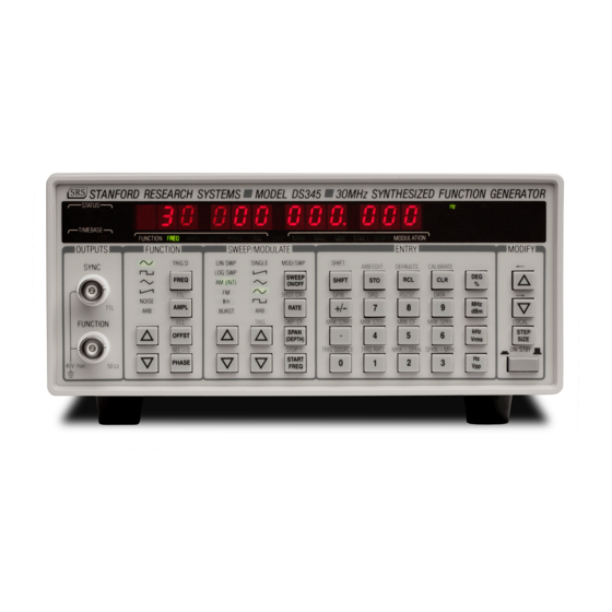
- Page 1 MODEL DS345 Synthesized Function Generator 1290-D Reamwood Avenue Sunnyvale, California 94089 Phone: (408) 744-9040 • Fax: (408) 744-9049 email: info@thinkSRS.com • www.thinkSRS.com Copyright © 1993-99, 2009, 2012, 2015, 2016 by SRS, Inc. All Rights Reserved. Revision 2.3 (12/2016)
-
Page 3: Table Of Contents
DS345 Synthesized Function Generator Table of Contents GPIB and RS232 Setup 2-26 Condensed Information Self-Test and Autocal 2-27 SRS Symbols Safety and Use Arbitrary Waveform Editing 2-29 Specifications Edit Menu 2-29 Abridged Command List Point Format Editing 2-30 Point Format Example... - Page 4 DS345 Synthesized Function Generator For More Info Performance Tests Frequency Accuracy DS345 Circuitry Amplitude Accuracy Circuit Description DC Offset Accuracy Bottom PC Board Subharmonics Power Supplies Spurious Signals Microprocessor System Harmonic Distortion Display and Keyboard Phase Noise Ribbon Cable, Trigger and Sync...
- Page 5 DS345 Synthesized Function Generator...
- Page 6 SELECTOR set for the wrong ac line voltage or if the wrong fuse is installed. LINE VOLTAGE SELECTION LINE FUSE The DS345 operates from a 100V, 120V, Verify that the correct line fuse is installed 220V, or 240V nominal ac power source before...
- Page 7 Specifications SPECIFICATIONS FREQUENCY RANGE Waveform Maximum Freq Resolution Sine 30.2 MHz 1 µHz Square 30.2 MHz 1 µHz Ramp 100 KHz 1 µHz Triangle 100 KHz 1 µHz Noise 10 MHz (Gaussian Weighting) Arbitrary 10 MHz 40 MHz sample rate OUTPUT Source Impedance 50 Ω...
- Page 8 Specifications Triangle, Ramp, Arbitrary: ±3% > 5Vpp ±5% < 5Vpp DC OFFSET Range: ±5V (limited such that |V | + |V | ≤ 5 V) ac peak Resolution: 3 digits (VAC = 0) Accuracy: 1.5% of setting + 0.2 mV (DC only) ±0.8 mV to ±80 mV depending on AC and DC settings WAVEFORMS Sinewave Spectral Purity...
-
Page 9: Specifications
Specifications DSB Carrier: < -35db typical at 1 kHz modulation rate (DSBSC) Ext Input: ±5V for 100% modulation, 100 kW impedance. FREQUENCY MODULATION Source: Internal (sine, square, triangle, ramp) Rate: 0.001 Hz to 10 kHz 1 µHz to 30.2 MHz (100 kHz for triangle or ramp) Span: PHASE MODULATION Source:... - Page 10 Specifications GENERAL Interfaces RS232-C (300 to 19200 Baud, DCE) and IEEE-488.2 with free DOS Based Arbitrary Waveform Software All instrument functions are controllable over the interfaces. Weight 10 lbs Dimensions 8.5" x 3.5" x 13" (WHL) Power 50 VA, 100/120/220/240 Vac 50/60 Hz viii...
-
Page 11: Abridged Command List
AMOD? i Allows downloading a i point arbitrary modulation waveform if the modulation type is AM, FM, or PM. After execution of this query the DS345 will return the ASCII value 1. The binary waveform data may now be downloaded. - Page 12 Allows downloading a j point arbitrary waveform of format i. i = 0 = point format, i= 1 = vector format. After execution of this query the DS345 will return the ascii value 1. The binary waveform data may now be downloaded.
-
Page 13: Getting Started
DOWN ARROW key will decrease the value by the current step size. If the entered value is outside of the allowable limits for the parameter the DS345 will beep and dis- play an error message. -
Page 14: Frequency Sweep
The next example sets up a linear frequency sweep with markers. The Frequency Sweep DS345 can sweep the output frequency of any function over any range of al- lowable output frequencies. There are no restrictions on minimum or maxi- mum sweep span. The sweep time may range from 1 ms to 1000 s. The DS345 also has two independent rear-panel markers that may be used indi- cate specific frequencies in the sweep. -
Page 15: Tone Bursts
This function allows zooming in on any feature in the sweep without entering the frequencies. This example demonstrates the DS345's tone burst capability. The DS345 Tone Bursts can produce a burst of 1 to 30,000 cycles of any of its output functions. The bursts may be triggered by the internal rate generator, the line frequency, a front panel button, or an external rising or falling edge. - Page 16 Getting Started Set the modulation type to BURST. 4) Press [SWEEP MODE DOWN ARROW] three times. Set the number of pulses in the burst to 10. Any 5) Press [SHIFT][BRST CNT]. Then [1][0][Hz]. of the units keys may be used to terminate the en- try.
-
Page 17: Introduction To Dds
Introduction to Direct Digital Synthesis Direct Digital Synthesis (DDS) is a method of generating very pure wave- Introduction forms with extraordinary frequency resolution, low frequency switching time, crystal clock-like phase noise, and flexible modulation. As an introduction to DDS let's review how traditional function generators work. Frequency synthesized function generators typically use a phase-locked loop Traditional Generators (PLL) to lock an oscillator to a stable reference. - Page 18 Control Figure 2: DS345 Block Diagram A block diagram of the DS345 is shown in Figure 2. The heart of the DS345 is a 40 MHz crystal clock. This clock is internally provided, but may be phase locked to an external reference. The 40 MHz clock controls the DDS345 ASIC, waveform RAM, and high-speed 12bit DAC.
- Page 19 The output of the power amplifier passes through a series of three step atten- uators (6, 12, and 24 dB) that set the DS345's final output amplitude. The post amplifier attenuators allow internal signal levels to remain as large as possible, minimizing output noise and signal degradation.
- Page 20 Introduction...
- Page 21 PHASE 40V max. FREQ The power switch turns the DS345 on and off. In the STBY position power is 1) Power Switch maintained to the DS345's internal oscillator, minimizing warmup time. The modify keys permit the operator to increase or decrease the displayed 2) MODIFY Keys parameter value.
-
Page 22: Ds345 Features
These six LEDs indicate the DS345's status. The LED functions are: 10) Status LEDs name function The DS345 is in GPIB remote state. The STEP SIZE key re- turns local control. The DS345 has requested service on the GPIB interface. Flashes on RS232/GPIB activity. -
Page 23: Rear Panel Features
RS232 (DCE, 8d, 0p, 2s bits) For use by qualified laboratory personnel only. This contains the DS345's fuse and line voltage selector. Use a 1 amp fuse 1) Power Entry Module for 100/120 volt operation, and a 1/2 amp fuse for 220/240 volt operation. To set the line voltage selector for the correct line voltage first remove the fuse. - Page 24 The shield of this output is tied to that of the function output and may be floated up to ±40V relative to earth ground. This output generates a 0 - 10 V ramp that is synchronous with the DS345's Sweep Output frequency sweep.
- Page 25 The fourth and last section describes front panel editing of arbitrary waveforms. When the power is first applied to the DS345 the unit will display its serial Power-On number and ROM version for about three seconds. The DS345 will then ini- tiate a series of self-tests of the circuitry and stored data.
-
Page 26: Function Setting
If the function is set to ARB the frequency displayed is the sampling fre- quency of the arbitrary waveform. This number is independent of the usual frequency; it is the dwell time that the DS345 spends on each point in an ar- bitrary waveform. This sampling frequency must be an integer submultiple of the the 40 MHz clock frequency. -
Page 27: Amplitude
Pressing [AMPL] two times displays the invert enable option. Use the UP/DOWN MODIFY keys to enable or disable the inversion. The output of the DS345 may be set to a DC level by entering an amplitude D.C. Only of 0V. When the amplitude is set to zero the A.C. waveform will be off and the DS345 may be used as a DC voltage source. -
Page 28: Dc Offset
Function Setting TTL levels are 5 V with a 2.5V offset (the output will swing between 0 and +5V). Pressing [SHIFT][ECL] sets the output amplitude and offset to ECL values. ECL Settings ECL levels are 1 V with a -1.3V offset (the output will swing between -1.8V and -0.8V). -
Page 29: Sweeps And Modulation
If the selected modulation is illegal (for example, FM frequen- cy out of range for the function) the DS345 will display an error message and not enable the modulation. The erroneous value must be changed before the modulation is turned on. -
Page 30: Modulation Rate
Modulation and Sweeps If no waveform has been downloaded when this modulation is enabled the message "arb corrupt" will be displayed (see the ARBITRARY MODULATION section). Single Ramp Triangle Sine Square None Type Linear Swp Log Swp Burst Table 1: Allowed modulation waveforms for each modulation type Pressing [RATE] displays and sets the modulation rate. -
Page 31: Amplitude Modulation
Modulation and Sweeps AMPLITUDE MODULATION The DS345 has the ability to amplitude modulate its function output with both Introduction the internal modulation generator and an external analog voltage. The inter- nal modulation generator may modulate the output with a sine, square (pulse modulation), triangle, ramp, or arbitrary modulation pattern. -
Page 32: Frequency Modulation
Modulation and Sweeps FREQUENCY MODULATION The DS345 is capable of frequency modulating any of its output functions, Introduction except NOISE and ARB, using its internal modulation generator. The modu- lation waveform may be a sine, square (FSK), triangle, ramp, or an arbitrary pattern. -
Page 33: Phase Modulation
Modulation and Sweeps PHASE MODULATION The DS345 is capable of phase modulating any of its output functions, ex- Introduction cept NOISE and ARB, using its internal modulation generator. The modula- tion waveform may be a sine, square (PSK), triangle, ramp, or arbitrary pat- tern (see ARBITRARY MODULATION section for information about ARB patterns). -
Page 34: Burst Modulation
100 kHz for triangles and ramps, and no limits for ARBs. When a trig- ger signal is received the DS345 initiates a burst starting at a specific point (phase) in the output waveform, outputs the exact number of programmed waveform cycles, and then stops. -
Page 35: Frequency Sweeps
0.001 and 1000 sec- onds. The DS345 has an analog SWEEP output that may be used to drive an x-y recorder or oscilloscope, a TTL BLANK/LIFT output that can lift a chart... -
Page 36: Sweep Markers
If the span is positive the DS345 will sweep up, if it is negative the DS345 will sweep down. The MODIFY keys may be used to change the span: pressing [MODIFY UP] will double the span, while pressing [MODIFY DOWN] divides the span in half. -
Page 37: Sweep Outputs
Modulation and Sweeps The markers may also be set by the center frequency and span (width) of the Marker Center and Span marked region. Pressing [SHIFT][MRK CF] and [SHIFT][MRK SPAN] respec- tively sets the center frequency and span. The center frequency may have any value from 1 µHz to 30.2 MHz range. -
Page 38: Trigger Generator
[SHIFT][TRIG RATE]. The rate may be set to any value in the range 0.001 Hz to 10 kHz with two digits of resolution. The TRIG'D LED indicates the DS345's trigger status. Each time a trigger is TRIG'D LED accepted the TRIG'D LED flashes green. If the DS345 is triggered again be- fore the previous BURST/SWEEP is complete, the TRIG'D LED will flash red, indicating a trigger error. -
Page 39: Arbitrary Modulation Patterns
To use arbitrary modulation, the modulation type must be set to AM, FM, or PM, and an arbitrary pattern must then be sent to the DS345. If no pattern has been loaded the DS345 will display the message "arb corrupt". [SWEEP ON/OFF] enables the arbitrary modulation. - Page 40 Modulation and Sweeps DS345 AS A PULSE GENERATOR The DS345 can be easily used as a pulse generator. Pulse widths down to Introduction 500 ns with rise/fall times of 30 ns and repetition rates up to 10 kHz internally and 500 kHz externally triggered are possible. You can even do bursts of groups of pulses (each pulse has to be the same width and separated by 1 pulse width).
-
Page 41: Instrument Setup
9600 GPIB Address Power on Status Clear To store the DS345's current setup press [STO] followed by a location num- Storing Setups ber in the range of 0 to 9. Pressing any of the UNITS key to enter the loca- tion number, the message "Store Done"... - Page 42 SRQ LED will light. The SRQ LED will go off after the host computer does a serial poll of the DS345. The user service re- quest is in addition to the usual service requests based on status conditions (see PROGRAMMING section for details).
-
Page 43: Self-Test And Autocal
DS345's circuits. Pressing any UNITS key when the AUTOCAL menu item is displayed starts the calibration. Autocal is disabled during the first two minutes after power on to allow the DS345 to warm up (an error will be displayed if autocal is started before this time). - Page 44 DS345 Setup The items not calibrated are the frequency dependent amplitude corrections, the doubler carrier null, the attenuator ratios, and the clock frequency. These values are stable and should not need adjustment except during the yearly recalibration. 2-28...
-
Page 45: Arbitrary Waveform Editing
Sampling Rate waveform sampling frequency. This number is not related to the normal waveform frequency, but is the time that the DS345 dwells at each point in the arbitrary waveform. This sampling frequency must be an integer submulti- ple of the the 40 MHz clock frequency. That is, 40 MHz/N where N = 1,2,3... -
Page 46: Point Format Editing
Arbitrary Waveform Editing The format of the data display is shown below for both point and vector for- Data Display mat. The data line has two values in both formats. The left value is the point/ vertex number, indicating which point/vertex is being edited. The right hand value is the data for that point. - Page 47 ARROW]. Delete point #4. y value becomes ------ (no data). 13) Press [CLR]. We only entered 4 data points. The DS345 will 14) DONE! automatically fill in the 4 trailing zero values when it loads the waveform RAM. The DS345 only adds enough zeroes to make the total number of points equal to 8, and none if there are 8 or more points.
-
Page 48: Vector Format Editing
0 (the start of memory) the DS345 will automatically add a vertex at 0,0. If the x value has no data (be- fore a value has been entered, for example) the data will be displayed as five dashes (-----). - Page 49 5) Press [SHIFT][RIGHT ARROW] then [5][0] Activate x value and set to 50. We will let the [UNITS]. DS345 add the 0,0 vertex automatically. 6) Press [STEP SIZE] then [2][0][0][UNITS]. Switch to y value and set to 200. 7) Press [SHIFT][LEFT ARROW] then [MODIFY Select vertex number and increment to vertex #1.
- Page 50 Arbitrary Waveform Editing 11) Press [SHIFT][LEFT ARROW], [MODIFY UP Select vertex # and increment to 3, then select y ARROW], [SHIFT][RIGHT ARROW], [2][0][0][0] value and set to 2000. [UNITS]. 12) Press [STEP SIZE], then [2][2][5][UNITS]. Select x value and set to 225. 13) Press [SHIFT][LEFT ARROW], [MODIFY UP Select vertex # and increment to 4, then select x ARROW], [SHIFT][RIGHT ARROW], [2][7][5]...
-
Page 51: Programming The Ds345
GPIB menu (type [SHIFT][GPIB] twice) and can be set between 0 and 30. The DS345 is configured as a DCE ( transmit on pin 3, receive on pin 2) and RS232 Communications supports CTS/DTR hardware handshaking. The CTS signal (pin 5) is an out- put indicating that the DS345 is ready, while the DTR signal (pin 20) is an in- put that is used to control the DS345's transmitting. - Page 52 If the buffer fills up the DS345 will hold off handshaking on the GPIB and attempt to hold off handshaking on RS232. If the buffer overflows the buffer will be cleared and an error reported.
- Page 53 Programming Commands The four letter mnemonic in each command sequence specifies the com- DETAILED COMMAND LIST mand. The rest of the sequence consists of parameters. Multiple parame- ters are separated by commas. Parameters shown in {} are optional or may be queried while those not in {} are required.
- Page 54 Programming Commands ed and the frequency will be set to the maximum allowed for the new func- tion. If modulation is enabled and the current modulation parameters are in- compatible with the selected function the modulation will be disabled and then the function will be set.
- Page 55 Programming Commands query returns the current modulation waveform. Waveform SINGLE SWEEP RAMP TRIANGLE SINE SQUARE NONE The value i = 5 = ARB may only be set for AM, FM, and PM. The arbitrary waveform must be downloaded via the AMOD? query. If no waveform has been downloaded and modulation is enabled with the waveform set to ARB an error will be generated.
- Page 56 Programming Commands center freq + span/2. A negative span will generate a downward sweep, from maximum to minimum frequency. The SPAN? query returns the current sweep span. The SPCF command sets the sweep center frequency to x Hertz. An error SPCF (?) x will be generated if the sweep frequency is less than or equal to zero or greater than allowed by the current function.
- Page 57 Second, the commands are queries- that is, after the command is received and processed the DS345 will return the ascii value 1 indicating that it is ready to receive the binary data stream. When using these commands the program should wait for return val- ue before sending the binary data.
- Page 58 DS345 an error will be gener- ated. If the data sent is valid and the DS345's function is set to ARB the waveform will automatically be output. Otherwise, the function must be set to ARB to output the downloaded waveform.
- Page 59 0 to 9. If the stored setting is corrupt or has never been stored an execution error will be generated. The *RST common command resets the DS345 to its default configurations. *RST The *SAV command saves the current instrument settings as setting number...
- Page 60 Sync Error. The sync signal generator has failed. Doubler Error. The frequency doubler has failed. The $ATD? query uses the DS345 A/D converter to measure the voltage on $ATD? i,j analog channel i. The parameter j = 0 returns the raw data value, j=1 returns the value corrected for the A/D's offset, and j=2 returns the value corrected for the A/D's offset and gain errors.
- Page 61 0 to 509, while k may range from -32768 to +32767. This command will generate an error if calibration is not enabled. NOTE: this command will alter the calibration of the the DS345. To correct the calibra- tion the factory calibration bytes may be recalled (see the $FCL command).
-
Page 62: Status Byte Definitions
DDS status byte. On power on the DS345 may either clear all of its status enable registers or maintain them in the state they were in on power down. The action taken is set by the *PSC command and allows things such as SRQ on power up . - Page 63 The Ext Clk bit will be set whenever the DS345 is locked to an external clock source. The Warmup bit will be set and remain set after the warmup period has expired. The rest of the bits in this register are set when the corresponding event occurs and remain set until cleared by reading this status byte or by the *CLS command.
- Page 64 Programming Commands 3-14...
- Page 65 To successfully interface the DS345 to a PC via the GPIB interface, the in- strument, interface card, and interface drivers must all be configured proper- ly. To configure the DS345, the GPIB address must be set in the GPIB menu. The default GPIB address is 19; use this address unless a conflict occurs with other instruments in your system.
-
Page 66: Arbitrary Am Modulation
EXAMPLE 1: Arbitrary Amplitude Modulation. This program downloads an arbitrary AM pattern to the DS345. The modulating waveform is a sine wave. The range of amplitude values will be -100% to +100% of full output, making DSBSC modulation. The pro- gram calculates the AM pattern values, sets the modulation type to AM, modulation waveform to ARB, down- loads the pattern, and enables modulation. -
Page 67: Arbitrary Fm Modulation
(ds345,cmd,strlen(cmd)); EXAMPLE 2: Arbitrary Frequency Modulation. This program downloads an arbitrary FM pattern to the DS345. The modulating waveform is a sine wave. The program calculates the FM pattern values, sets the modulation type to FM, modulation waveform to ARB, downloads the pattern, and enables modulation. -
Page 68: Arbitrary Pm Modulation
This program downloads an arbitrary PM pattern to the DS345. The modulating waveform is a sine wave. Since the DS345 expects a list of phase changes we calculate the initial phase of the waveform and then take differences from that phase. - Page 69 /* arb modulation command */ ibwrt (ds345,cmd,strlen(cmd)); ibrd (ds345,cmd,40); /* read back reply before sending data */ ibwrt (ds345,(char *)data,(long)4*number+4); /* number of bytes = 4 per data point + 4 for checksum */ sprintf (cmd,"MENA1\n"); /* turn modulation on */ ibwrt (ds345,cmd,strlen(cmd));...
- Page 70 (cmd,"LDWF?0,%d\n",number); /* command to load waveform */ ibwrt (ds345,cmd,strlen(cmd)); ibrd (ds345,cmd,40); /* read back reply before sending data */ ibwrt (ds345,(char *)data,(long)2*number+2); /* number of bytes = 2 per data point + 2 for checksum */ sprintf (cmd,"FUNC5\n"); /* arb wf output */ ibwrt (ds345,cmd,strlen(cmd));...
- Page 71 (cmd,"LDWF?1,%d\n",number); /* command to load waveform */ ibwrt (ds345,cmd,strlen(cmd)); ibrd (ds345,cmd,40); /* read back reply before sending data */ ibwrt (ds345,(char *)data,(long)4*number+2); /* number of bytes = 4 per data point(x and y) + 2 for checksum */ sprintf (cmd,"FUNC5\n"); /* arb wf output */ ibwrt (ds345,cmd,strlen(cmd));...
- Page 72 Program Examples 3-22...
-
Page 73: Troubleshooting
The "Autocal" procedure should be run af- ter the unit warms up (see INSTRUMENT SETUP section). The following lists explain all of the error messages that the DS345 can gen- ERROR MESSAGES erate. The messages are divided into operational errors, self-test errors, and autocal errors. - Page 74 Load CS Error The checksum calculated by the DS345 is different than that received from the computer on downloading of ARB waveform or modulation. Check that the computer is sending the correct # points and calculating sum correctly.
- Page 75 The output voltage is outside of 0.01V to 10V range. These errors may occur during the DS345's self- test. In general, these mes- Self-Test Errors sages indicate DS345 hardware problems. If the errors occur repeatedly the unit may have an electrical problem. The messages are listed alphabetically, also listed is the status value returned by the *TST? command.
- Page 76 Cal Dly Err The DS345 is not warmed up. Wait until warmed up for at least two minutes befor starting autocal. DAC Off Err The waveform DAC's output offset calibration did not converge or went out- side the ±50mV allowed range.
- Page 77 19, and so it is a good idea to use this address when writing pro- grams for the DS345. Any address from 0 to 30 may be set in the GPIB menu. To check the GPIB address, press [SHIFT][GPIB] twice to view the GPIB address.
- Page 78 Troubleshooting...
-
Page 79: Performance Tests
The first set of tests test the basic functionality of the DS345 from the front panel. The second set of tests actually measure the DS345's specifications. The results of each test may be recorded on the test sheet at the end of this section. - Page 80 Performance Tests FUNCTIONAL TESTS These simple tests verify that the DS345's circuitry is functional. They are not intended to verify the DS345's specifications. This test verifies the functionality of the front panel digits, LED's, and buttons. Front Panel Test 1) Turn on the DS345 while holding down [FREQ]. A single segment of the leftmost digit should light.
- Page 81 1) Connect the DS345's output to the oscilloscope input and terminate in 50Ω. 2) Set the DS345 to sine wave, 1MHz, 10Vpp. Set the scope to 2V/div verti- cal and 1µs/div horizontal. 3) Verify that the DS345's output is about 10V pk-to-pk.
- Page 82 Performance Tests...
-
Page 83: Frequency Accuracy
These tests are intended to measure the DS345's conformance to its published specifications. The test re- sults may be recorded on the test sheet at the end of this section. Allow the DS345 at least 1/2 hour to warm up, run the DS345's autocal procedure, and proceed with the tests. - Page 84 50Ω impedance no terminator is needed). Connect the thermal converter output to the voltmeter using the most sensitive voltmeter range since the nominal signal level is about 7mV DC. Allow the DS345 at least 1/ 2 hour to warm up.
-
Page 85: Dc Offset Accuracy
1) Connect the DS345 to the RF spectrum analyzer. Set the DS345 to sine wave, +23.98dBm (10Vpp), 0V offset. 2) Set the DS345 to to 102 kHz. Set the spectrum analyzer to 51 kHz center frequency, 10 kHz span. The carrier amplitude at 51 kHz should be less than... -
Page 86: Spurious Signals
DS345 to 50 kHz. Verify that the harmonics are at least -55 dBc. 5) Set the DS345 to 500 kHz, 5 MHz, 15 MHz, and 30 MHz and verify that all harmonics are at least -45 dBc, -35 dBc, -25 dBc, and -25 dBc respectively. -
Page 87: Phase Noise
10 MHz, > +10 dBm. 3) Record the AC voltage reading. 4) Set the DS345 to 10.0 MHz. Measure the DC signal from the mixer. Use the DS345's PHASE control to minimize the DC voltage value. 5) Set the voltmeter to AC and measure the mixer output. Calculate the ratio of this voltage to that obtained in step 3 ( dB = 20 log (V )). -
Page 88: Square Wave Rise Time
SQUARE WAVE SYMMETRY This test measures the symmetry of the square wave output. specification: < 1% of period + 4ns 1) Connect the output of the DS345 to the A input of the time interval counter and terminate into 50Ω. Set the DS345 to square wave, 1 MHz, 5 Vpp. -
Page 89: Square Wave Symmetry
Performance Tests DS345 PERFORMANCE TEST RECORD Serial Number: __________ Date:____________ Tested By:______________ Comments: Pass Fail Functional Tests Front Panel Test _____ _____ Self Tests _____ _____ Sine Wave _____ _____ Square Wave _____ _____ Amplitude Flatness _____ _____ Output Level... - Page 90 Performance Tests sine, 8.001 MHz, 3 Vrms ____________ sine, 10.001 MHz, 3Vrms ____________ sine, 12.001 MHz, 3 Vrms ____________ sine, 14.001 MHz, 3 Vrms ____________ sine, 16.001 MHz, 3 Vrms ____________ sine, 18.001 MHz, 3 Vrms ____________ Tolerance ±6.3% of X ___________ __________ (0.937X)
-
Page 91: Am Envelope Distortion
Performance Tests sine, 5 MHz, 1 Vpp ____________ -35 dBc sine, 15 MHz, 1 Vpp ____________ -25 dBc sine, 30 MHz, 1 Vpp ____________ -25 dBc Phase Noise sine, 10.001 MHz, 13 dBm = V1 ____________ sine, 10.0 MHz, 13 dBm = V2 ____________ noise = 20 log (V2/V1) - 6 dB... -
Page 92: Calibration
DS345's RAM. Recalibration of the DS345 involves deter- mining the values of the calbytes and storing the new values in RAM. The calbyte values at the time of the DS345's production are also stored in ROM and may be recalled at any time. - Page 93 Calibration DS345 CALBYTES Number Name Autocal Meaning Oscillator Cal Tunes Oscillator. Range = 0 - 4095 +5 V Ref Cal Value of +5 ref voltage. Value = 32768 *(Vref/5.00) ADC Gain ADC Gain correction. ADC Offset ADC Offset correction. DC Offset Gain DC ouput offset gain fix.
-
Page 94: Necessary Equipment
The oscillator calibra- tion should be done after this adjustment. 1) Connect the DS345's 10 MHz output to the frequency counter input. The counter should use the frequency standard for its timebase. Be sure that the... -
Page 95: Output Amplifier Bandwidth
2) Connect the output of the DS345 to the oscilloscope with a 50Ω termina- tor. Set the DS345 to square wave, 8 Vpp, 100 Hz. Set the scope to 2 V/div vertical and 5 ms/div horizontal. Adjust R639 for the squarest output wave- form. -
Page 96: Harmonic Distortion
Harmonic Distortion Adjust tion. A complete calibration is necessary after this adjustment. 1) Set the DS345 to sine wave, 8 Vpp, 15 kHz. Connect the DS345's output to the FFT analyzer with a 50Ω terminator. Set the FFT analyzer to display from DC to 100 kHz. -
Page 97: Calibration
= old calbyte + 65536 in the following calculations. 1) Connect the output of the DS345 to a DC voltmeter. Do not use a 50Ω terminator. Set the DS345 to sine wave, 1 kHz, 0 Vpp, 5 V offset. -
Page 98: Carrier Null Calibration
DS345's frequency range. This calibration must be done before the amplitude calibrations. 1) Set the DS345 to sine wave, 1 kHz, 8 Vpp, 0 V offset. Connect the DS345's output to the FFT spectrum analyzer using a 50Ω terminator. Set the analyzer to display 0 to 2 kHz. -
Page 99: Sinewave Amplitude
DS345's frequency range. The carrier null calibration should be done be- fore this calibration. 1) Set the DS345 to sine wave, 1 kHz, 3 Vrms, 0 V offset. Set the frequency step size to 312500 Hz. Connect the DS345's output to the thermal convert- er and the thermal conveter output to the DC voltmeter. -
Page 100: Square Wave Symmetry
DS345's frequency range. This calibration should be done after the square wave amplitude calibration. 1) Set the DS345 to square wave, 1 kHz, 10 Vpp. Connect the DS345's out- put to the counter with a 50Ω terminator. Set the DS345's frequency step size to 312500 Hz. - Page 101 Calibration 6-10...
-
Page 102: Arbitrary Waveform Software
The Arbitrary Waveform Composer (AWC) is a program that allows the user to create or import arbitrary waveforms and then download the waveform to the DS345. AWC has the ability to create arbitrary waveforms, store waveforms to disk, edit stored waveforms, and download waveforms to the DS345. AWC can edit and download waveforms that it has created or waveforms created from other sources and then stored as an ASCII text file. - Page 103 Throughout this example the Send Data and Trigger menus were disabled. This is because the communications parameters have not been set. Select the RS232/GPIB submenu from the Set DS345 menu to set the communication parameters according to your specific hardware configuration. See the Set DS345 menu description for more information on establishing communication with the DS345.
-
Page 104: Hardware Requirements
AWC is designed to run on Windows systems running XP/2000/Me/98. The DS345 Synthesized Function Generator must be equipped with option 01, GPIB and RS232 interfaces. AWC communicates with the DS345 though an RS232 interface or a National Instruments hardware implementation of the GPIB interface. -
Page 105: Waveform Menu
| + |V ac peak command only changes the data in AWC's waveform database. The waveform must be reloaded into the DS345 for the change to take effect. Waveform menu The Waveform menu is the key to creating new waveforms and modifying existing ones. -
Page 106: Send Data Menu
This selection sends the current arbitrary waveform to the DS345. When the waveform is sent to the DS345 the state of the DS345 is set to match that of AWC. That is, the DS345's sampling rate and trigger parameters are set to match the settings in AWC. -
Page 107: Trigger Menu
The default setting is continuous waveforms. The six trigger choices are the five that are internal to the DS345 plus the PC mouse. If PC mouse is selected a trigger button will appear on the AWC screen. The DS345 will trigger each time the button is clicked. -
Page 108: Data File Format
Arbitrary Waveform Composer DATA FILE FORMAT AWC data is saved as ASCII text. Each line of the file consists of a single numerical value followed by a carriage return/linefeed. The first line is the number of data points in the waveform. The second line is the sampling frequency in Hz. - Page 109 Arbitrary Waveform Composer...
-
Page 110: Ds345 Circuitry Circuit Description
BOTTOM PC BOARD POWER SUPPLIES (SHEET 1 OF 7) All of the DS345 circuitry is referenced to an internal ground that is floating from the chassis ground. The interface board (see sheet 5) contains the only circuitry that is earth-ground referenced. -
Page 111: Ribbon Cable, Trigger And Sync
GPIB AND RS232 INTERFACES (SHEET 5 OF 7) The field installable interface PCB offers RS232 and GPIB communications that are optically isolated from the DS345's floating circuitry. All connections are made via JP501. The RS232 interface is handled by U512, which generates the required RS232 levels from the 5-volt interface supply. -
Page 112: Output Amplifier
DS345 Circuitry OUTPUT AMPLIFIER (SHEET 6 of 7) The output amplifier takes the differential signal from the DDS top board and generates the single-ended 20-volt P-P signal that is fed to the output attenu- ators. The amplifier has a rise time of about 10 ns (35 MHz bandwidth) to preserve pulse shapes, and after series 50-ohm resistor R636 can deliver +/- 10 volts into a 50-ohm load. -
Page 113: Top Pc Board
DS345 Circuitry TOP PC BOARD RIBBON CABLE, ADCs, and DACs (SHEET 1 OF 7) JP100 and JP101 are the system interface and top board power supply con- nectors to the bottom board, respectively. U109A is half of a 12-bit DAC that is used to generate analog voltages for system control. -
Page 114: Dds Asic And Memory
DS345 Circuitry U206. The sampling phase detector is made up primarily of U206. The selected in- put at U206 pin 1 or 13 is chopped by the RCO output of U202, which serves as a sampling gate. The gated output at pin 4 is then filtered by R235, C220, R236 and C221 to form a control voltage to be presented to the oscillator va- ractor. -
Page 115: Dds Waveform Dac
DS345 Circuitry U412B generates a 12-bit resolution analog output that is used to fix up the offset present in the frequency doubler multiplier (see sheet 6). The 50 kHz Bessel filter at the output of U413A pin 1 again is an anti-aliasing filter for this output. - Page 116 DS345 Circuitry signal inputs) to help cancel out the 2f component in the output. The network of resistors connected to the multiplier X inputs serves to offset the control voltage so that the compliance of the multiplier inputs is not approached, minimizing distortion.
- Page 117 DS345 Circuitry...
-
Page 118: Component Parts List
Component Part List Bottom PC Board and Front Panel Parts List Ref No. SRS Part No. Value Description BT200 6-00001-612 BR-2/3A 2PIN PC Battery C 100 5-00023-529 Cap, Monolythic Ceramic, 50V, 20%, Z5U C 101 5-00192-542 22U MIN Cap, Mini Electrolytic, 50V, 20% Radial C 102 5-00100-517 2.2U... - Page 119 Component Part List C 146 5-00262-548 .01U AXIAL Capacitor, Ceramic, 50V,+80/-20% Z5U AX C 147 5-00262-548 .01U AXIAL Capacitor, Ceramic, 50V,+80/-20% Z5U AX C 148 5-00262-548 .01U AXIAL Capacitor, Ceramic, 50V,+80/-20% Z5U AX C 149 5-00262-548 .01U AXIAL Capacitor, Ceramic, 50V,+80/-20% Z5U AX C 150 5-00262-548 .01U AXIAL...
- Page 120 Component Part List 3-00012-306 GREEN LED, Rectangular 3-00012-306 GREEN LED, Rectangular 3-00377-305 GL9ED2 LED, Rectangular, Bicolor 3-00455-310 GREEN COATED LED, Coated Rectangular 3-00012-306 GREEN LED, Rectangular D 10 3-00012-306 GREEN LED, Rectangular D 11 3-00012-306 GREEN LED, Rectangular D 12 3-00012-306 GREEN LED, Rectangular...
- Page 121 Component Part List D 105 3-00062-340 KBP201G/BR-81D Integrated Circuit (Thru-hole Pkg) D 106 3-00011-303 LED, T1 Package D 108 3-00062-340 KBP201G/BR-81D Integrated Circuit (Thru-hole Pkg) D 109 3-00226-301 1N5822 Diode D 110 3-00004-301 1N4148 Diode D 111 3-00004-301 1N4148 Diode D 112 3-00004-301 1N4148...
- Page 122 Component Part List 7-00366-701 DS345 BOTTOM Printed Circuit Board 7-00368-701 DS345 FP Printed Circuit Board Q 100 3-00177-321 2N2222 Transistor, TO-18 Package Q 200 3-00140-325 2N2369A Transistor, TO-92 Package Q 201 3-00026-325 2N5210 Transistor, TO-92 Package Q 202 3-00026-325 2N5210...
- Page 123 Component Part List R 114 4-00021-401 1.0K Resistor, Carbon Film, 1/4W, 5% R 115 4-00032-401 100K Resistor, Carbon Film, 1/4W, 5% R 118 4-00032-401 100K Resistor, Carbon Film, 1/4W, 5% R 119 4-00081-401 Resistor, Carbon Film, 1/4W, 5% R 120 4-00021-401 1.0K Resistor, Carbon Film, 1/4W, 5%...
- Page 124 Component Part List R 609 4-00031-401 Resistor, Carbon Film, 1/4W, 5% R 610 4-00021-401 1.0K Resistor, Carbon Film, 1/4W, 5% R 611 4-00021-401 1.0K Resistor, Carbon Film, 1/4W, 5% R 612 4-00714-401 Resistor, Carbon Film, 1/4W, 5% R 613 4-00714-401 Resistor, Carbon Film, 1/4W, 5% R 614 4-00191-407...
- Page 125 Resistor, Metal Film 1/2W, 1%, 50ppm S 300 6-00096-600 MINI Misc. Components SO202 1-00026-150 28 PIN 600 MIL Socket, THRU-HOLE 7-00340-740 DS345-1 Keypad, Conductive Rubber SW10 2-00023-218 DPDT Switch, Panel Mount, Power, Rocker SW30 2-00008-207 SPSTX4 Switch, DIP T 100...
- Page 126 Component Part List U 305 3-00406-340 74HCT374 Integrated Circuit (Thru-hole Pkg) U 306 3-00406-340 74HCT374 Integrated Circuit (Thru-hole Pkg) U 400 3-00166-340 74HC153 Integrated Circuit (Thru-hole Pkg) U 401 3-00316-340 74HC151 Integrated Circuit (Thru-hole Pkg) U 402 3-00044-340 74HC244 Integrated Circuit (Thru-hole Pkg) U 403 3-00044-340 74HC244...
- Page 127 7-00344-720 DS345-9 Fabricated Part 7-00345-720 DS345-10 Fabricated Part 7-00347-720 DS345-12/-13 Fabricated Part 7-00348-720 DS345-14 Fabricated Part 7-00440-701 DS345 RR PANEL Printed Circuit Board 7-00680-720 PS300-52 Fabricated Part 7-00721-709 DS345-19 Lexan Overlay 9-00458-917 DS335/340/345 Product Labels Z 100 0-00158-070 60MM 24V Fans, &...
- Page 128 Component Part List C 104 5-00023-529 Cap, Monolythic Ceramic, 50V, 20%, Z5U C 105 5-00023-529 Cap, Monolythic Ceramic, 50V, 20%, Z5U C 106 5-00023-529 Cap, Monolythic Ceramic, 50V, 20%, Z5U C 107 5-00023-529 Cap, Monolythic Ceramic, 50V, 20%, Z5U C 108 5-00023-529 Cap, Monolythic Ceramic, 50V, 20%, Z5U C 109...
- Page 129 Component Part List C 413 5-00002-501 100P Capacitor, Ceramic Disc, 50V, 10%, SL C 414 5-00074-515 .015U Capacitor, Mylar/Poly, 50V, 10%, Rad C 415 5-00064-513 .0047U Capacitor, Mylar/Poly, 50V, 5%, Rad C 416 5-00263-513 .0012U Capacitor, Mylar/Poly, 50V, 5%, Rad C 417 5-00074-515 .015U...
- Page 130 Component Part List C 574 5-00262-548 .01U AXIAL Capacitor, Ceramic, 50V,+80/-20% Z5U AX C 575 5-00262-548 .01U AXIAL Capacitor, Ceramic, 50V,+80/-20% Z5U AX C 576 5-00262-548 .01U AXIAL Capacitor, Ceramic, 50V,+80/-20% Z5U AX C 580 5-00262-548 .01U AXIAL Capacitor, Ceramic, 50V,+80/-20% Z5U AX C 581 5-00262-548 .01U AXIAL...
- Page 131 Component Part List C 635 5-00017-501 Capacitor, Ceramic Disc, 50V, 10%, SL C 640 5-00019-501 Capacitor, Ceramic Disc, 50V, 10%, SL C 641 5-00019-501 Capacitor, Ceramic Disc, 50V, 10%, SL C 642 5-00256-530 2.8-12.5P Capacitor, Variable, Misc. C 643 5-00106-530 9.0-50P Capacitor, Variable, Misc.
- Page 132 Res. Network, SIP, 1/4W,2% (Isolated) P 700 4-00011-441 Pot, Multi-Turn Trim, 3/8" Square Top Ad P 701 4-00013-441 Pot, Multi-Turn Trim, 3/8" Square Top Ad 7-00365-701 DS345 TOP Printed Circuit Board 7-00819-701 DDS FIX Printed Circuit Board Q 203 3-00018-324 MRF904...
- Page 133 Component Part List R 18 4-01463-461 Thick Film, 5%, 200 ppm, Chip Resistor R 20 4-01439-461 Thick Film, 5%, 200 ppm, Chip Resistor R 21 4-01439-461 Thick Film, 5%, 200 ppm, Chip Resistor R 22 4-01439-461 Thick Film, 5%, 200 ppm, Chip Resistor R 100 4-00031-401 Resistor, Carbon Film, 1/4W, 5%...
- Page 134 Component Part List R 231 4-00021-401 1.0K Resistor, Carbon Film, 1/4W, 5% R 232 4-00072-401 Resistor, Carbon Film, 1/4W, 5% R 233 4-00021-401 1.0K Resistor, Carbon Film, 1/4W, 5% R 235 4-00021-401 1.0K Resistor, Carbon Film, 1/4W, 5% R 236 4-00031-401 Resistor, Carbon Film, 1/4W, 5% R 237...
- Page 135 Component Part List R 445 4-00032-401 100K Resistor, Carbon Film, 1/4W, 5% R 446 4-00239-407 Resistor, Metal Film, 1/8W, 1%, 50PPM R 447 4-00239-407 Resistor, Metal Film, 1/8W, 1%, 50PPM R 600 4-00204-407 Resistor, Metal Film, 1/8W, 1%, 50PPM R 601 4-00204-407 Resistor, Metal Film, 1/8W, 1%, 50PPM R 602...
- Page 136 Component Part List R 712 4-00097-401 Resistor, Carbon Film, 1/4W, 5% R 713 4-00097-401 Resistor, Carbon Film, 1/4W, 5% R 714 4-00030-401 Resistor, Carbon Film, 1/4W, 5% R 715 4-00130-407 1.00K Resistor, Metal Film, 1/8W, 1%, 50PPM R 716 4-00130-407 1.00K Resistor, Metal Film, 1/8W, 1%, 50PPM R 717...
- Page 137 Component Part List U 110 3-00088-340 LF353 Integrated Circuit (Thru-hole Pkg) U 111 3-00088-340 LF353 Integrated Circuit (Thru-hole Pkg) U 200 3-00294-340 AD96685 Integrated Circuit (Thru-hole Pkg) U 201 3-00442-301 MV104 Diode U 202 3-00333-340 74HC161 Integrated Circuit (Thru-hole Pkg) U 205 3-00105-340 LM741...
- Page 138 Component Part List 6-00098-614 T37-6 Iron Powder Core Optional PC Board Parts List Ref No. SRS Part No. Value Description C 500 5-00192-542 22U MIN Cap, Mini Electrolytic, 50V, 20% Radial C 501 5-00010-501 270P Capacitor, Ceramic Disc, 50V, 10%, SL C 502 5-00023-529 Cap, Monolythic Ceramic, 50V, 20%, Z5U...
- Page 139 U 523 3-00446-340 6N137 Integrated Circuit (Thru-hole Pkg) 0-00079-031 4-40X3/16 M/F Standoff 0-00500-000 554808-1 Hardware, Misc. 7-00720-709 DS345-18 Lexan Overlay Miscellaneous and Chassis Assembly Parts List Ref No. SRS Part No. Value Description U 202 3-00345-342 27C512-120 EPROM/PROM, I.C. 0-00150-026...
Need help?
Do you have a question about the DS345 and is the answer not in the manual?
Questions and answers