
Related Manuals for Portwell PEB-2737VLA Series


Summary of Contents for Portwell PEB-2737VLA Series
- Page 1 PEB-2737VLA Series Embedded System Board User's Manual Version 1.0b Copyright © Portwell, Inc., 2009. All rights reserved. All other brand names are registered trademarks of their respective owners.
-
Page 2: Table Of Contents
Preface Table of Contents How to Use This Manual Chapter 1 System Overview ....................... 1-1 1.1 Introduction ..........................1-1 1.2 Check List ............................. 1-2 1.3 Product Specification ........................1-2 1.3.1 Mechanical Drawing ......................1-4 1.4 System Architecture ........................1-6 Chapter 2 Hardware Configuration ................... 2-1 2.1 Jumper Setting .......................... -
Page 3: How To Use This Manual
BIOS setting, and OS diagnostics. The content of this manual is subject to change without prior notice. These changes will be incorporated in new editions of the document. Portwell may make supplement or change in the products described in this document at any time. -
Page 4: Chapter 1 System Overview
System Overview Chapter 1 System Overview Introduction Powell Inc., a world-leading innovator in the Industrial PC (IPC) market and a member of the Intel® Communications Alliance, has launched its new PEB-2737VLA in response to market demand for a simplified embedded system board (ESB) that combines a smaller footprint, lower power consumption, robust computing power and with longevity support. -
Page 5: Check List
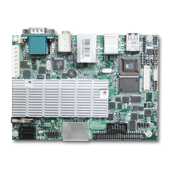
System Overview Check List The PEB-2737VLA package should include the following items: One PEB-2737VLA embedded system board One ATX Power Cable One 2-in-1 Heatsink One Installation Resources CD Title If any of these items is damaged or missing, please contact your vendor and keep all packing materials for future replacement and maintain. - Page 6 System Overview On-board Ethernet One Gigabit Ethernet (10/100/1000 Mbits/sec) LAN ports using Realtek PCI- Expressx1interface GbE Ethernet Controller On Board I/O - Rear I/O ‧Line-Out ‧MIC-In ‧Four USB ports ‧PS/2 keyboard & mouse ‧One DB-9 support RS-232 ‧One DB-15 VGA port ‧Fast Ethernet port (RJ45) - Internal I/O ‧One 44-pin IDE connector...
-
Page 7: Mechanical Drawing
System Overview - Operating temperature: 0 to 60 °C - Storage temperature: -20 to 80 °C - Relative Humidity 5% to 95%, non-condensing 1.3.1 Mechanical Drawing PEB-2737VLA User’s Manual... - Page 8 System Overview PEB-2737VLA User’s Manual...
-
Page 9: System Architecture
System Overview System Architecture All of details operating relations are shown in PEB-2737VLA System Block Diagram. PEB-2737VLA Block Diagram PEB-2737VLA User’s Manual... -
Page 10: Chapter 2 Hardware Configuration
Hardware Configuration Chapter 2 Hardware Configuration This chapter gives the definitions and shows the positions of jumpers, headers and connector. All of the configuration jumpers on PEB-2737 are in the proper position. The default settings are indicated with a star sign (). Jumper Setting For users to customize PEB-2737’s features. - Page 11 Hardware Configuration JP1 : Clear CMOS Function Open Normal operation Short Clear CMOS JP2 : 5V / 3.3V Panel power selection Function 1-2 Short 3.3V 2-3 Short 5V JP3 : Microcontroller programming Function 1-2, 3-4, 5-6 Short Normal operation 1-2, 3-4, 5-6 Open Programming microcontroller JP4 : 5V / 3.3V backlight enable pin power level selection...
-
Page 12: Connector Allocation
Hardware Configuration Connector Allocation I/O peripheral devices are connected to the interface connectors. Connector Function List Connector Function Remark SATA port 1 SDIO Port (Support SD 1.1 and MMC 4.0 only) PATA 44-Pin (IDE) Temperature Sense SATA port 2 Serial port 2 USB port 6,7 USB port 0,2 8 bit GPIO... - Page 13 Hardware Configuration CN2 : SDIO Connector Pin No. Signal Description Pin No. Signal Description SDIO_DATA0 +3.3V SDIO_DATA1 SDIO_CLK SDIO_DATA2 SDIO_CMD SDIO_DATA3 +3.3V SDIO_DATA4 SDIO_DATA5 SDIO_CD# SDIO_DATA6 SDIO_WP SDIO_DATA7 CN3 : Hard Disk 44-pin Connector Pin No. Signal Description Pin No. Signal Description R_PLT_RST# PDD7...
- Page 14 Hardware Configuration CN5 : SATA Port 2 Pin No. Signal Description SATATX+ SATATX- SATARX+ SATARX- CN6 : Serial port 2 Connector Pin No. Signal Description Pin No. Signal Description DCD1# RXD1# TXD1# DTR1# DSR1# RTS1# CTS1# RI1# CN7 : USB Port6&Port7 Header Pin No.
- Page 15 Hardware Configuration CN9 : 8 bit GPIO Header Pin No. Signal Description Pin No. Signal Description LPC_GP10 LPC_GP14 LPC_GP11 LPC_GP15 LPC_GP12 LPC_GP16 LPC_GP13 LPC_GP17 CN10 : LVDS Panel Interface Connector Pin No. Signal Description Pin No. Signal Description LVDSA_DATA0+ LVDSA_DATA0- LVDSA_DATA1+ LVDSA_DATA1- LVDSA_DATA2+...
- Page 16 Hardware Configuration CN12 : Power Connector Pin No. Signal Description +5V Standby +12V PS_ON# CN13 : LPC Debug Port Header Pin No. Signal Description Pin No. Signal Description LAD0 +3.3V LAD1 PLT_RST# LAD2 LFRAME# LAD3 LPC_PCID CN14 : Giga Ethernet RJ45 with 2 port USB Jack Pin No.
- Page 17 Hardware Configuration CN16 : PS/2 Keyboard/Mouse Pin No. Signal Description Pin No. Signal Description KB_DATA MS_DATA KB_CLK MS_CLK CN17 : USB Port4&Port5 Jack Pin No. Signal Description Pin No. Signal Description USBD5- USBD4- USBD5+ USBD4+ CN18 : Audio Jack Pin No. Signal Description Stereo line out Bottom...
- Page 18 Hardware Configuration CN21 : Fan Connector Pin No. Signal Description +12V CN22 : DDR2 SO-DIMM 200Pin Connector CN23 : Compact Flash connector Pin No. Signal Description Pin No. Signal Description Ground Data 3 Data 11 Data 4 Data 12 Data 5 Data 13 Data 6 Data 14...
- Page 19 Hardware Configuration PEB-2737VLA User’s Manual 2-10...
-
Page 20: Chapter 3 System Installation
System Installation Chapter 3 System Installation This chapter provides you with instructions to set up your system. The additional information is enclosed to help you set up onboard device and handle Watch Dog Timer (WDT) and operation of GPIO in software programming. ®... -
Page 21: Main Memory
System Installation Main Memory PEB-2737VLA provides one 200-pin DDR2 SO-DIMM socket which supports 400/533 DDR2-DRAM as main memory, Non-ECC (Error Checking and Correcting), non-register functions. The maximum memory size can be up to 2GB capacity. For system compatibility and stability, do not use memory module without brand. Memory configuration can be either one double-sided DIMM in either one DIMM socket or one single-sided SO-DIMM in socket. -
Page 22: Chipset Component Driver
System Installation 3.4.1 Chipset Component Driver The chipset on PEB-2737VLA is a new chipset that a few old operating systems might not be able to recognize. To overcome this compatibility issue, for Windows Operating Systems such as Windows XP/VISTA, please install its INF before any of other Drivers are installed. -
Page 23: Wdt Function
2 seconds” is the recommendation due to the limitation of Winbond W83627DHG WDT. You can call Portwell support center for reference. The value read back from CR_T indicates the counting down value instead of the original T . - Page 24 System Installation There are two I/O ports as I/O access window for configuring WDT, 1) IO port 0x2E is H/W strapped and named as EFIR (Extended Function Index Register, for identifying CR index number) 2) IO port 0x2F is H/W strapped and named as EFDR (Extended Function Data Register, for accessing desired CR) <<...
-
Page 25: Gpio
System Installation Step(4) : LD8_CRF7_bit[7,6]P[0,0] Not allow K/B and Mouse’s interrupts to reload WDT timer. outportb ( EFIR , 0xF7 ) ; al_char1 = inportb ( EFDR ) & 0x3F ; // CRF7_bit[7,6]P[0,0] outportb ( EFIR , 0xF7 ) ; outportb ( EFDR , al_char1 ) ;... -
Page 26: Pin Assignment
System Installation Refer to the W83627DHG data sheet to configure both input / output port, SGP30~37, by programming W83627DHG GPIO registers. Users can configure each individual port to be an input or output port by programming respective bit in selection register (0 =output, 1 = input). Invert port value by setting inversion register (0 = non -inverse, 1 = inverse). - Page 27 System Installation (1) Initialize W83627DHG multiplex pins to SGP32~34 function enter_Superio_CFG(); d = GET_CFG(0x2A); d = d & 0xFD; Set_CFG(0x2A, d); // Pin 89,90 function selected by CR2C d = GET_CFG(0x2C); d = d & 0x1F; Set_CFG(0x2C, d); // Declare Pin88,89,90 as GPIO function (2) Point to LD9 ( for SGP30~37 GPIO port registers ) and activate its function Set_CFG(0x07, 0x09);...
-
Page 28: Chapter 4 Bios Setup Information
BIOS Setup Information Chapter 4 BIOS Setup Information PEB-2737VLA is equipped with the AMI BIOS stored in Flash ROM. These BIOS has a built-in Setup program that allows users to modify the basic system configuration easily. This type of information is stored in CMOS RAM so that it is retained during power-off periods. -
Page 29: Main
BIOS Setup Information Main Use this menu for basic system configurations, such as time, date etc. AMI BIOS, Processor, System Memory These items show the firmware and hardware specifications of your system. Read only. System Time The time format is <Hour> <Minute> <Second>. Use [+] or [-] to configure system Time. -
Page 30: Advanced
BIOS Setup Information Advanced Use this menu to set up the items of special enhanced features. PEB-2737VLA User’s Manual... - Page 31 BIOS Setup Information CPU Configuration These items show the advanced specifications of your CPU. Read only. Hardware Prefetcher The Hardware Prefetcher looks the streams of data. The data is prefetched into L2 from external memory. Disabling of this item may impact processor performance. The choice: Disabled, Enabled.
- Page 32 BIOS Setup Information Execute-Disable Bit Capability Disabled force the XD feature flag to always return 0. The choice: Disabled, Enabled. Intel (R) SpeedStep (tm) tech Disabled / Enabled GV3 tech function. The choice: Disabled, Enabled. IDE Configuration The IDE Configuration the IDE devices, such as hard disk drive or CD-ROM drive. It uses a separate sub menu to configure each hard disk drive (Master and Slave).
- Page 33 BIOS Setup Information Primary / Secondary IDE Master / Slave While entering setup, BIOS auto detects the presence of IDE devices. This displays the status of auto detection of IDE devices. [Type] Press PgUp/<+> or PgDn/<-> to select [Manual], [None] or [Auto] type. You can use [Manual] to define your own drive type manually.
- Page 34 BIOS Setup Information Hard Disk Write Protect Disabled/Enabled device write protection, this will be effective only if device is accessed through BIOS. The choice: Disabled, Enabled. IDE Detect Time Out (Sec) Select the time out value for detecting ATA/ATAPI device (s). The choice: 0, 5, 10, 15, 20, 25, 30, 35.
- Page 35 BIOS Setup Information Serial Port 2 Mode This item allows users to select Infrared transmission mode. The choice: Normal, IrDA, ASK IR. WatchDog Timer Set This function will determine watch dog timer during the range of 10 Sec., 20 Sec., 30 Sec., 40 Sec., 1 Min., 2 Min., and 4 Min.
- Page 36 BIOS Setup Information SYSFAN PWM Control This setting allows users to control the fan speed by changing the duty cycle of the fan PWM (Pulse-Width Modulation) output. The choice: 0 ~ 255. ACPI Configuration Select for Advanced ACPI Configuration. PEB-2737VLA User’s Manual...
- Page 37 BIOS Setup Information General ACPI Configuration Suspend mode This item specifies the power saving modes for ACPI function. If your operating system supports ACPI, you can choose to enter the Standby mode in S3 (STR) fashion through the setting of this field. Options are: [S3 (STR)] The S3 sleep mode is a lower power state where the information of system configuration and open applications/ files is saved to main memory that remains powered while most other hardware components turn off to save energy.
- Page 38 BIOS Setup Information Advanced ACPI Configuration Advanced ACPI Configuration settings, Use this section to configure additional ACPI options. ACPI Version Features Enable RSDP pointers to 64-bit Fixed System Description Tables. The choice: ACPI v1.0 / ACPI v2.0 / ACPI v3.0. ACPI APIC support Include ACPI APIC table pointer to RSDT pointer list.
- Page 39 BIOS Setup Information Chipset ACPI Configuration Chipset ACPI related Configuration settings, Use this section to configure additional ACPI options. APIC ACPI SCI IRQ Enable / Disable APIC ACPI SCI IRQ. The choice: Disabled, Enabled. USB Device Wake From S3/S4 Enable / Disable USB device Wake from S3/S4 mode. The choice: Disabled, Enabled.
- Page 40 BIOS Setup Information MPS Configuration Configure the Multi-Processor Table. MPS Revision This field allows you to select which MPS (Multi-Processor Specification) version to be used for the operating system. You need to select the MPS version supported by your operating system. To find out which version to use, consult the vendor of your operating system.
- Page 41 BIOS Setup Information PCI Express Configuration Configure PCI Express Support. Active State Power-Management PCI Express L0s and L1 link power states. The choice: Disabled, Enabled. PEB-2737VLA User’s Manual 4-14...
- Page 42 BIOS Setup Information Smbios Configuration SMBIOS Configuration Menu. Smbios Smi Support SMBIOS SMI Wrapper support for PnP Func 50h-54h. The choice: Disabled, Enabled. PEB-2737VLA User’s Manual 4-15...
- Page 43 BIOS Setup Information USB Configuration Legacy USB Support Set to [Enabled] if you need to use any USB 1.1/2.0 device in the operating system that does not support or have any USB 1.1/2.0 driver installed, such as DOS and SCO Unix. The choice: Disabled, Enabled, Auto.
-
Page 44: Pcipnp
BIOS Setup Information PCIPnP Advanced PCI/PnP setting wrong values in below sections may cause system to malfunction. PEB-2737VLA User’s Manual 4-17... -
Page 45: Clear Nvram
BIOS Setup Information Clear NVRAM Clear NVRAM during System Boot. The choice: No, Yes. Plug & Play O/S No: lets the BIOS configure all the devices in the system. Yes: lets the operating system configure Plug and Play (PnP) devices not required for boot if your system has a Plug and Play operating system. -
Page 46: Boot
BIOS Setup Information Reserved Memory Size Select Size of memory block to reserve for legacy ISA devices. The choice: Disabled, 16K, 32K, 64K. Boot Use this menu to specify the priority of boot devices. PEB-2737VLA User’s Manual 4-19... - Page 47 BIOS Setup Information Boot Settings Configuration Quick Boot Enabling this setting will cause the BIOS power-on self test routine to skip some of its tests during boot up for faster system boot. The choice: Disabled, Enabled. Quiet Boot This BIOS feature determines if the BIOS should hide the normal POST messages with the motherboard or system manufacturer's full-screen logo.
- Page 48 BIOS Setup Information AddOn ROM Display Mode This item is used to determine the display mode when an optional ROM is initialized during POST. When set to [Force BIOS], the display mode used by AMI BIOS is used. Select [Keep Current] if you want to use the display mode of optional ROM.
- Page 49 BIOS Setup Information Interrupt 19 Capture Interrupt 19 is the software interrupt that handles the boot disk function. When enabled, this BIOS feature allows the ROM BIOS of these host adaptors to "capture" Interrupt 19 during the boot process so that drives attached to these adaptors can function as bootable disks.
-
Page 50: Security
BIOS Setup Information Security Use this menu to set supervisor and user passwords. Supervisor Password / Change Supervisor Password Supervisor Password controls access to the BIOS Setup utility. These settings allow you to set or change the supervisor password. User Password / Change User Password User Password controls access to the system at boot. -
Page 51: Chipset
BIOS Setup Information Chipset This menu controls the advanced features of the onboard Northbridge and Southbridge. PEB-2737VLA User’s Manual 4-24... - Page 52 BIOS Setup Information North Bridge Configuration Primary Graphic Adapter Select which graphics controller to use as the primary boot device. The choice: IGD, PCIe/IGD. Internal Graphics Mode Select Select the amount of system memory used by the internal graphics device. The choice: Disabled, Enabled, 1MB, Enabled, 4MB, Enabled, 8MB.
- Page 53 BIOS Setup Information Boot Display Configuration Boot Display Device Use the field to select the type of device you want to use as the display(s) of the system. The choice: Auto, Integrated LVDS, External DVI/HDMI, External TV, External CRT, External LVDS. Local Flat Panel Scaling Allows you to determine how various resolutions appear on your screen.
- Page 54 BIOS Setup Information Disabled- The image isn't scaled at all, but instead your LCD display will run at its maximum resolution and the image will display in the centre of your LCD display. This may result in a black border around the sides of the image. Flat Panel Type The choice: 640x480 (generic), 800x600 (generic), 1024x768 (generic), 640x480 (NEC 8.4”), 800x600 (NEC 9”), 1024x600 (TMD 5.61”), 1024x600 (Samsung...
- Page 55 BIOS Setup Information USB 2.0 Controller Set to [Enabled] if you need to use any USB 2.0 device in the operating system that does not support or have any USB 2.0 driver installed, such as DOS and SCO Unix. USB Client Controller The choice: Enabled, Disabled.
-
Page 56: Exit
BIOS Setup Information Exit This menu allows you to load the BIOS default values or factory default settings into the BIOS and exit the BIOS setup utility with or without changes. Save Changes and Exit Exit System Setup and save your changes to CMOS. Pressing <Enter> on this item asks for confirmation: Save changes to CMOS and exit the Setup Utility. -
Page 57: Chapter 5 Troubleshooting
Troubleshooting Chapter 5 Troubleshooting This chapter provides a few useful tips to quickly get PEB-2737VLA running with success. As basic hardware installation has been addressed in Chapter 3, this chapter will primarily focus on system integration issues, in terms of BIOS setting, and OS diagnostics. - Page 58 BIOS setting that Portwell has highly endorsed. As a matter of fact, users can load the default BIOS setting any time when system appears to be unstable in boot up sequence.
- Page 59 Troubleshooting A quick review of the basic IRQ mapping is given below for your reference. IRQ# Description IRQ #0 System Counter IRQ #1 Keyboard IRQ #2 Programmed Controller IRQ #3 COM2 IRQ #4 COM1 IRQ #5 Sound, Network, USB 1.0/1.1 UHCI Controller IRQ #6 Floppy Disk Controller IRQ #7...
-
Page 60: Faq
Question: How can I connect my PEB-2737VLA series to panel? Answer: First of all, you need to read the Panel spec and Inverter spec to understand which type of panel you will use on PEB-2737VLA series; different panel will connect to different connector; LVDS interface is CN10. -
Page 61: Appendix A System Memory Address Map
Appendix A System Memory Address Map Each on-board device in the system is assigned a set of memory addresses, which also can be identical of the device. The following table lists the system memory address used. Memory Area Size Device Description 0000-003F Interrupt Area 0040-004F... -
Page 62: Appendix B Interrupt Request Lines (Irq)
Appendix B Interrupt Request Lines (IRQ) Peripheral devices can use interrupt request lines to notify CPU for the service required. The following table shows the IRQ used by the devices on-board. IRQ# Current Use Default Use IRQ 0 System ROM System Timer IRQ 1 System ROM...
Need help?
Do you have a question about the PEB-2737VLA Series and is the answer not in the manual?
Questions and answers