
Subscribe to Our Youtube Channel
Related Manuals for Daewoo DVD-T6300N


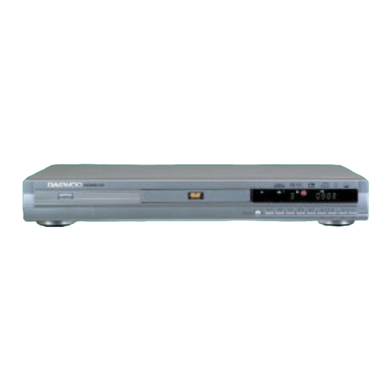
Summary of Contents for Daewoo DVD-T6300N
-
Page 1: Table Of Contents
DVD PLAYER DVD-T6300N SERVICE MANUAL CONTENTS DVD PLAYER Component Descriptions 1. Precautions 2. Reference Information 3. Product Specification 4. Operating Instructions 5. Disassembly and Reassembly 6. Troubleshooting 7. Electrical Part List 8. Block Diagram 9. PCB Diagrams 10. Wiring Diagram 11. -
Page 2: Precautions
1. Precautions 1-1 Safety Precautions 1) Before returning an instrument to the customer, and then in the OFF position, measure from a always make a safety check of the entire known earth ground (metal water pipe, conduit, instrument, including, but not limited to, the etc.) to all exposed metal parts of the following items: instrument (antennas, handle brackets, metal... - Page 3 Safety Precautions (5) within the limits specified, there is the possibility the AC power cord for damage. of a shock hazard, and the instrument must be re-pared and rechecked before it is returned to 5) Components, parts, and/or wiring that appear to the customer.
-
Page 4: Servicing Precautions
1-2 Servicing Precautions CAUTION : Before servicing Instruments covered (3) The components used in the unit have a by this service manual and its supplements, read specified flame resistance and dielectric and follow the Safety Precautions section of this strength. manual. -
Page 5: Esd Precautions
1-3 ESD Precautions Electrostatically Sensitive Devices (ESD) its protective package until immediately before you are ready to install it. (Most replacement ESD Some semiconductor (solid state) devices can be devices are packaged with leads electrically damaged easily by static electricity. shorted together by conductive foam, aluminum Such components... -
Page 6: Reference Information
2. Reference Information 2-1 Component Descriptions 2-1-1 Fiber Optic Transmitting Module for Digital Audio Equipments (TOTX178) Recommended Operating Conditions Item Symbol Min. Typ. Max. Unit Supply Voltage 4.75 5.25 High Level Input Voltage Low Level Input Voltage *This is an optional output. - Page 7 Component Descriptions 2-1-2 NTSC/PAL Digital Video Encoder (ADV7170)
- Page 8 Component Descriptions...
- Page 9 Component Descriptions...
- Page 10 Component Descriptions 2-1-3 DVD Processor Chip (Swan-2 ES4318) Features Single-chip DVD video decoder in a 208-pin PQFP package Supports MPEG-1 system and MPEG-2 program streams Programmable multimedia processor architecture Compatible with Audio CD, Video CD, VCD 3.0, and Super Video CD(SVCD) DVD Navigation 1 Built-in Content Scrambling System(CSS) Audio...
- Page 11 Component Descriptions Functional Description...
- Page 12 Component Descriptions Pinout Diagram...
- Page 13 Component Descriptions Pin Descriptions Name Number Definition 1, 9, 18, 27, 35, 44, 51, 59, 68, 75, 83, 92, 99, 104, 111, 3.65 V ± 150 mv. 121, 130, 139, 148, 157, 164, 172, 183, 193, 201 LA[21:0] 23:19,16:10,7:2,207:204 Device address output. 8,17,26,34,43,52,60,67,76,84,91,98,103, 112,120,129,1 Ground.
- Page 14 Component Descriptions Name Number Definition Horizontal synch screen video HSYNCH# interface, programmable for rising or falling edge, active low. HD[15:0] 141:140, 137:131, 128:122 Host data bus HCS1FX# Host select 1. HCS3FX# Host select 3. HIOCS16# Device 16-bit data transfer. HA[2:0] 158, 155:154 Host address bus.
- Page 15 Component Descriptions 2-1-4 DIGITAL-TO-ANALOG STEREO AUDIO CONVERTER (CS4391)
- Page 16 Component Descriptions...
- Page 17 Component Descriptions...
- Page 18 Component Descriptions...
- Page 19 Component Descriptions 2-1-5 8-BIT MTP MICROCONTROLLER (W78LE52) Features Fully static design 8-bit CMOS microcontroller 256 bytes of on-chip scratchpad RAM 8 KB electrically erasable/programmable MTP-ROM 64 KB program memory address space 64 KB data memory address space Four 8-bit bi-directional ports Three 16-bit timer/counters One full duplex serial port(UART) Watchdog Timer...
- Page 20 Component Descriptions Block Diagram Absolute Maximum Ratings PARAMETER SYMBOL MIN. MAX. UNIT DC Power Supply VDD-VSS -0.3 +7.0 Input Voltage VSS -0.3 VDD +0.3 Operating °C Temperature Storage Temperature +150 °C...
- Page 21 Component Descriptions Pin Descriptions SYMBOL DESCRIPTIONS EXTERNAL ACCESS ENABLE: This pin forces the processor to execute out of external ROM. It should be kept high to access internal ROM. The ROM address and data will not be presented on the bus if EA pin is high and the program counter is within on-chip ROM area.
- Page 22 Component Descriptions 2-1-6 Serial EEPROM, 2K (256 x 8) (AT24C02) Features • Low-Voltage and Standard-Voltage Operation – 5.0 (V CC = 4.5V to 5.5V) – 2.7 (V CC = 2.7V to 5.5V) – 2.5 (V CC = 2.5V to 5.5V) –...
- Page 23 Component Descriptions 2-1-7 4-Megabit (512K x 8) FLASH (A29040) Features • 5.0V±40% for read and write operations • Access time –70max • Current –20 mA typical active read current –30 mA typical program/erase current –1µA typical CMOS Standby • Flexible sector architecture –...
- Page 24 Component Descriptions Block Diagram Pin Descriptions Absolute Maximum Ratings Ambient Operating Temperature ...... -55°C to +125°C Storage Temperature ........…. -65°C to +150°C VOC Ground .……………………………………..-2.0V to +7.0V Output Voltage…………………………………… -2.0V to +7.0V...
- Page 25 Component Descriptions 2-1-8 256K X 16DYNAMIC RAM(T224162B) Features Industry-standard x 16 pinouts and timing functions. Single 5V power supply. All device pins are TTL-compatible. 512-cycle refresh in 8ms Refresh modes: /RAS only, /CAS BEFORE /RAS (CBR) and HIDDEN. Extended data-out (EDO) PAGE MODE access cycle. BYTE WRITE and BYTE READ access cycles.
- Page 26 Component Descriptions Block Diagram Pin Configurations...
- Page 27 Component Descriptions 2-1-9 1Mbit(x8) Multi-Purpose Flsh (SST39SF010A) Features Pin Configurations...
- Page 28 Component Descriptions Block Diagram Pin Descriptions...
- Page 29 Component Descriptions 2-1-10 System Reset Monolithic IC PST91XX Series Features Pin Assignment...
- Page 30 Component Descriptions 2-1-11 SP3721A : 6Ax DVD Analog Front End Chip Features Supports AGE and equalizer/filter for CD 3X to 32x and DVD 1x to 6x (with RX=8.2kohm) Low Power operation (350Mw typical @5V) Bi-directional serial port register access Register programmed power management (Sleep mode < 5mW ) Power supply range (4.4 to 5.5 V) Small footprint 64-lead TQFP Package Servo System...
- Page 31 Component Descriptions Channel 40 MHz bandwidth Supports individual RF inputs for DVD (Differential or single-ended) and CD (Single ended) Supports internet summing mode for RF signal for DVD and CD respectively Programmable attenuator (min;-24dB, 4-bit resolution) Fast attack/decay mode for rapid AGC recovery Low drift AGC hole circuitry Temperature compensated, exponential control AGC Supports external and internal AGC hold control function...
- Page 32 Component Descriptions Pin Configurations...
- Page 33 Component Descriptions Pin Description Table Name Number Type Description Input Pins DVDRFP, RF Signal Inputs. Differential RF signal attenuator input pins DVDRFN CORF RF Signal Input. Signal-ended RF signal attenuator input pin AIP, AIN 59,60 AGC Amplifier Inputs. Differential AGC amplifier input pins Analog Inputs for RF Single Buffer.
- Page 34 Component Descriptions Pin Description Table (continued) Name Number Type Description Analog Pins: The RF AGC integration capacitor CBYP, is connected BYP and VPA Differential Phase tracking LPF pin. An external capacitance is connected between this pin and the CP pin. Differential Phase tracking LPF pin.
- Page 35 Component Descriptions 2-1-12 DVD-ROM Controller Chip (M5705) Pin Configurations...
- Page 36 Component Descriptions Block Diagram...
- Page 37 Component Descriptions Pin Description Table Name Number Type Description Servo Date Slicer Interface Pins XSRFIN Analog RF signal input XSIPIN Inverting input pin of data slicer XSDSSLV Slice level output pin XSRSLINT Reference current setting pin for analog data slicer Servo DAC Interface Pins XSAWRC Output for enlarge VCO range.
- Page 38 Component Descriptions Pin Description Table (continued) Name Number Type Description Servo Control Interface Pins XSDFCT Defect detection signal input XSCSJ Chip selection signal for accessing control registers XSCLK Clock output for accessing control registers XSDATA Registers data input/output pin XSLDC Laser diode on/off control registers XSFGIN Motor Hall sensor input...
- Page 39 Component Descriptions Pin Description Table (continued) Name Number Description Type Microcontroller Interface Pins 48,50, XGPIO[3.0] These pins are used as general purpose I/O bus 51,52 XMP1-7 Internal microcontroller programmable I/O port 1.7 XMP1-6 Internal microcontroller programmable I/O port 1.6 XMP1-5 Internal microcontroller programmable I/O port 1.5 XMP1-4 Internal microcontroller programmable I/O port 1.4...
- Page 40 Component Descriptions Pin Description Table (continued) Pin Name Pin No. Type Description Host Interface Pins XHCS1J This pin is used to select the command block task file registers XHCS3J This pin is used to select the control block task file registers. XHIORJ Asserted by the host during a host I/O read operation XHIOWJ...
- Page 41 Component Descriptions Pin Description Table (continued) Pin Name Pin No Description Power Pins AVDD5 DS Analog Power for Data Slicer part AVDD5 DA Analog Power for DAC part AVDD5 AD Analog Power for ADC part AVDD5 PL Analog Power for Data PLL part 7,55,76 115,146 Power +3.3V for digital core logic and pad...
-
Page 42: Product Specification
3. Product Specifications Playback System DVD Video Video CD (1.1, 2.0, 3.0) SVCD and CVD CDDA CD-ROM with MP3 data Television Signal System NTSC/PAL Video Performance Video Out 1 Vpp / 75 ohm Y : 1 Vpp / 75 ohm S-Video Out C : 0.286 Vpp / 75 ohm Component Out... -
Page 43: Product Specifications
Product Specifications Connections Coaxial digital audio out Audio Analog out for 2-channel Component Video (Y,Pb,Pr) Composite Video out S-Video out Optical audio out X1(option) Power Supply Power Source AC 90~250V, 50/60Hz Power Consumption < 25 Watt Dimensions (W X H X D) 420 X 84 X 270 (mm ) Net Weight 3.6 Kg... -
Page 44: Operating Instructions
4. Operating Instructions 4-1 Basic Connections Connecting to audio equipment & TV Connecting to AUDIO SYSTEM TV set Audio equipment Method1: DVD Player + 2CH Streo Amplifer Method2: DVD Player + TV with Audio Input Jack(R.C) Connecting to TV (for VIDEO) Method1: DVD Player + TV with Video input Jack Method2: DVD Player + TV with S-video Jack... - Page 45 Operating Instructions Connecting to a decoder with a Dolby Digital or DTS processing TV set Coaxial audio cable (optional) To coaxial digital audio input Optical audio cable (optional) To optical digital audio input Decoder or Amplifier with Dolby Digital / dts Center Front Front...
- Page 46 Operating Instructions 4-2 Selecting Video MODE Press SETUP button and select VIDEO submenu on SETUP screen. After that, select TV type by pressing DOWN arrow button ( ▼) until desired TV mode is selected. For more information, refer to 7.2 Video on the Instruction Manual.
- Page 47 Operating Instructions 4-5 Selecting the desired MP3 title Use arrow button and select an MP3 title using the SELECT button then play will start automatically. When you know the title number, enter the MP3 title number using numeric buttons and press the SE- LECT button.
- Page 48 Operating Instructions 4-8 Slow Viewing When you want to view the disc contents very slowly in forward or reverse direction, you can do that by pressing the FF/SF button ( or the FR/SR button ( ) during pause mode. There are total 3 steps for DVD and VCD.
- Page 49 Operating Instructions 4-11 Selecting Angle Some DVD discs may contain scenes, which have been shot simul- taneously from a number of different angles. If the loaded disc su- pports multiple angles, you can see indicator on the fluorescent display and the TV screen. In the figure shown right, there are total 9 angles.
-
Page 50: Disassembly And Reassembly
5. Disassembly and Reassembly 5-1 Open Top Cabinet Fig. 1 Fig. 2 ① ② ③ ④ Let’s begin to disassemble ! Remove 4 screws on back top cabinet. Fig. 3 Fig. 4 ③ ④ ① ② Lift up the cabinet in direction of arrow. Remove 4 screws on the left and right side. -
Page 51: Rear Panel Removal
5-2 Rear Panel Removal Fig. 7 Fig. 8 ① ② ③ Remove 3 screws on the rear panel. Disassemble the power cord. Fig. 9 Fig. 10 Disjoint a rear panel from body, direction View of dissembly, top cabinet and rear of arrow. - Page 52 5-3 Ass’y Front –Panel Removal Fig. 11 Fig.12 Disconnect CN7 from Main PCB and Remove 1 screw. ‘CN3’ from SMPS PCB. Fig.13 Fig.14 ② ② ① ③ ① Remove 2 screws. Remove 3 screws. Fig.15 Emergency hole Insert a sharp point into emergency hole, and then push the tap in the hole in direction of arrow, open tray manually.
- Page 53 Ass’y Front –Panel Removal Fig. 16 Fig.17 Disassemble the door tray in direction of Release 2 taps on the left and right side arrow. from the bottom cabinet. Fig.18 Fig.19 Release 3 taps from the bottom cabinet. Disassemble the Ass’y Front Panel. Fig.
- Page 54 5-4 Jack PCB and SMPS Removal Fig. 22 Fig. 23 ① ② Remove 2 screws. Disconnect Jack PCB from Main PCB. Fig. 24 Fig. 25 ① ② ③ ④ Disconnect ‘CN5’ from Main PCB. Remove 4 screws, and dissemble SMPS. Fig.
- Page 55 5-5 Deck and Main PCB Removal Fig. 27 ③ ① ⑥ ② ④ ⑦ Remove 7 screws. ⑤ Fig. 28 Fig. 29 Disassemble Deck and Main PCB. When you take the DVD Player apart, you can see this picture.
-
Page 56: Troubleshooting
6. Troubleshooting ASDS An Appearance Requires Confirmation No power Insert the AC power plug securely into the power outlet. Make sure that the equipment is connected properly. No picture Make sure that the input setting for the TV is Video (AV). No sound Make sure that the equipment is connected properly. -
Page 57: Electrical Part List
7. Electrical Part List 1. Main board... -
Page 58: Electrical Part List
Electrical Part List... - Page 59 Electrical Part List 2. Front board Front Board SC Type Location Spec Pak' P C B A S S ' Y , F R O N T ( M / I ) (IR)INFRA RECIEVER L Type U2 TO-92 Q1 VFD DISPLAY FRONT POWER WIRE, 5PIN-5PIN(PCB), PCB IN WIRE CON2 FRONT SIGNAL WIRE, 11PIN-11PIN(PCB), PCB IN...
- Page 60 Electrical Part List 3.Jack board Location S100 Model (FOR USA) Spec Pak' Usa' A S S ' Y O P T I O N AAA, 1.5V, BATTERY A S S ' Y A C C E S O R Y 43KEY'S, REMOCON(IR) RCA CABLE(PIN CABLE) S-VHS CABLE...
- Page 61 Electrical Part List Location S100 Model (FOR USA) Spec Pak' Usa' PASS'Y,OUT_BD(SMD_bottom) 10 CHIP RES', 1/8W,1K Ohm J 0603 4 R729,R731,R734,R736 11 CHIP RES', 1/8W,220 Ohm J 0603 2 R744,R743 12 CHIP RES', 1/8W,20K Ohm J 0603 6 R751,R756,R761,R766,R771,R781 13 CHIP RES', 1/8W,3.3K Ohm J 0603 10 R716,R725,R741,R742,R753,R758,R763,R768,R773,R783 14 CHIP RES', 1/8W,3.9K Ohm J...
- Page 62 Electrical Part List 4.SMPS PART LIST...
- Page 63 Electrical Part List...
-
Page 64: Block Diagram
8. Block Diagram MAIN Board Block Diagram... -
Page 65: Pcb Diagrams
9. PCB Diagrams 9-1 Main PCB (TOP) - Page 66 PCB Diagrams 9-2 Main PCB (BOTTOM)
- Page 67 PCB Diagrams 9-3 JACK PCB (TOP)
- Page 68 PCB Diagrams 9-4 JACK PCB (BOTTOM)
- Page 69 PCB Diagrams 9 - 3 Front PCB (Component Side) 9 - 4 Front PCB (Solder Side)
- Page 70 PCB Diagrams 9-5 SMPS PCB (Top Side)
-
Page 71: Wiring Diagram
10. Wiring Diagram Wiring Diagram... -
Page 72: Schematic Diagrams
11. Schematic Diagrams 11-1 SMPS PCB Schematic Diagram... - Page 73 11-2 Front PCB Schematic Diagram...
- Page 74 11-3 Main PCB Schematic Diagram...
- Page 75 Main PCB Schematic Diagram...
- Page 76 Main PCB Schematic Diagram...
- Page 77 Main PCB Schematic Diagram...
- Page 78 Main PCB Schematic Diagram...
- Page 79 Main PCB Schematic Diagram...
- Page 80 Main PCB Schematic Diagram...
- Page 81 Main PCB Schematic Diagram...
- Page 82 Main PCB Schematic Diagram...
- Page 83 Main PCB Schematic Diagram...
- Page 84 Schematic Diagrams 11-4 JACK PCB Schematic Diagram...
- Page 85 11 JACK PCB Schematic Diagram...
-
Page 86: Oscillograms
Oscillograms 27MHz 2. ROM- DATA-BUS 3. RAM-DATA-BUS 4. 12C-CLK 5. 12C-DATA 6. HSYNC... -
Page 87: Oscillograms
Oscillograms 7. VSYNC 8. BCLK-DVD 9. LRCK-DVD 10. TSDO 11. MCLK 12. HOST-DATA... - Page 88 Oscillograms 13. HOST-CLK 14. HOST-CS 15. MC-DACO 16. MD-DACO 17. VFD-DATA 18. VFD-STB...
- Page 89 Oscillograms 19. VFD-CLK 20. COMPOSITE-OUT 21. COXIAL-OUT 22. OPTICAL-OUT 23. S-VIDEO 24. COMPONENT OUT...
- Page 90 MEMO...
Need help?
Do you have a question about the DVD-T6300N and is the answer not in the manual?
Questions and answers