Table of Contents
Advertisement
Service
Manual
REMARK : This service manual explains them by extracting specifications designed for the
model CDR500 only. The explanation for CD-R module "MAR775" (Loader : CDL4009' +
CD-R Main board) is not mentioned on this service manual.
The CD-R module infor mation is descr ibed in the ser vice manual of CD-R modules
<MAR770/MAR775>.
SECTION
MAIN UNIT
1.1 Servicing the CDR500 .......................................................................................................................... 1-1
1.2 TECHNICAL SPECIFICATIONS .......................................................................................................... 1-3
1.3 WARNINGS .......................................................................................................................................... 1-4
1.4 SERVICE HINTS .................................................................................................................................. 1-5
1.5 TOOLS ................................................................................................................................................. 1-5
1.6 SIAGNOSTIC SOFTWARE .................................................................................................................. 1-6
1.7 FAULTFINDING TREES .................................................................................................................... 1-10
1.8 FAULTFINDING GUIDE ..................................................................................................................... 1-16
1.9 WIRING DIAGRAM ............................................................................................................................ 1-33
1.10 BLOCK DIAGRAM .............................................................................................................................. 1-35
1.11 SCHEMATIC DIAGRAM AND PARTS LOCATION ............................................................................ 1-37
1.12 EXPLODED VIEW AND PARTS LIST ................................................................................................ 1-43
1.13 ELECTRICAL PARTS LIST ................................................................................................................ 1-46
MAR1250 ( CD MODULE )
2.1 WIRING DIAGRAM .............................................................................................................................. 2-1
2.2 SCHEMATIC DIAGRAM ....................................................................................................................... 2-3
2.3 PARTS LOCATION ............................................................................................................................ 2-11
2.4 EXPLODED VIEW AND PARTS LIST ................................................................................................ 2-15
2.5 ELECTRICAL PARTS LIST ................................................................................................................ 2-17
Please use this service manual with referring to the user guide ( D.F.U. ) without fail.
Printed in Japan
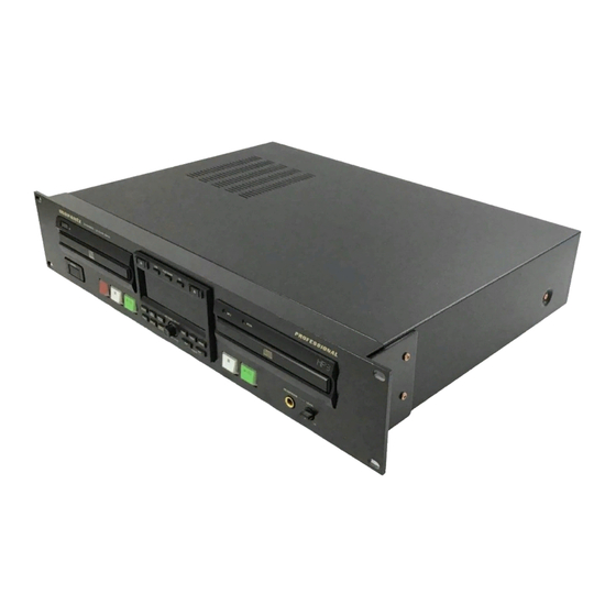
CD RECORDER/CD PLAYER CDR500
CDR
PLAY MODE
IR
Recordable
ReWritable
STORE
REC LEVEL/SELECT
STANDBY
ERASE
REC.
MENU
POWER
MODE
DELETE
FINAL
INPUT
CANCL
PUSH ENTER
TABLE OF CONTENTS
CDR500
CDR500 /
CD Recorder/CD Player
CD
TIME
TEXT
PROG
HEADPHONE
LEVEL
0
10
F1B, /N1B, /U1B
PAGE
R
388K855010 MIT
3120 785 22420
First Issue 2001.02
Advertisement
Table of Contents


Need help?
Do you have a question about the CDR500 F1B and is the answer not in the manual?
Questions and answers