
Related Manuals for Harman Kardon MAS 101


Summary of Contents for Harman Kardon MAS 101
- Page 1 MAS 101/102/111 Music system Service Manual...
- Page 2 CONTENTS 1. Specification ………………………………………………………………………………………………………….….1 2. Packing …………………………………………………………………………………………………………..………3 3. Front panel information ………………………………………………………………………………………………...4 4. Rear panel information …………………………………………………………………………………………………5 5. Remote control information ……………………………………………………………………………………………6 6. Block diagram …………………………………………………………………………………………………………...8 7. Wiring diagrams ………………………………………………………………………………………………………...9 8. IC spec ……………………………………………………………………………………………………………..…..10 9. Printed circuit boards ……………………………………………………………………………………………..…..87 10. Schematic diagram ………………………………………………………………………………………………..….97 11.
- Page 3 MAS SySteM Specifications System Power output 65 watts per channel, 20hz – 20khz, thd <0.07%, into 6 ohms, both channels driven Bandwidth 20hz – 35khz, –3dB System frequency response 20hz – 20khz, ±0.5dB Signal-to-noise ratio, a-weighted 90dB (analog inputs), 96dB (digital inputs) channel separation ≥65dB crosstalk between sources...
- Page 4 Signal-to-noise ratio “a” Wtg >96dBr; 22khz filter > 94dBr General Power requirement ac 230V/50hz (MaS 101/MaS 111); ac 120V/60hz (MaS 102) Power consumption <1W full standby (clock not activated); <2W standby (clock activated); 150W maximum (both channels driven) operating temperature 0°c to 40°c...
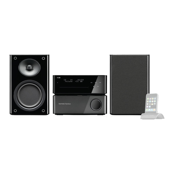
- Page 6 Front-Panel Controls MAS SySteM Controller and Amplifier note: controls are the same for all models. the MaS systems use touch-sensitive controls. to use a control, tap gently on its lit icon. USB Port A: connect a compatible uSB device here to enjoy playback of audio MP3 or WMa files.
- Page 7 Rear-panel connections MAS SySteM Controller FM Antenna Terminal: connect the included fM antenna wire here. Analog Audio Outputs: connect these outputs to the analog audio inputs of an audio recorder. When a source connected to the MaS system is playing, the signal will DAB Antenna Terminal (MAS 111 Only): connect the included daB antenna wire be available at these outputs for recording.
- Page 8 MAS SySteM Remote control functions Power Sleep Source Selectors display Settings Info Back time navigation enter Program/Memory clear check random eject fM Mode auto Store transport controls Volume +/– Preset/folder +/– Mute numeric keys –10 numeric Key +10 numeric Key •...
- Page 9 MAS SySteM Remote control functions Clear: clears the current preset station or a playlist entry. • Radio : to delete the current preset station, press the clear button while it is playing. • Playlist : While programming a playlist, press the clear button to delete the track just entered.
- Page 11 WIRING DIAGRAM...
- Page 12 Philips Semiconductors Product specification Hex inverter 74HCU04 FEATURES • Output capability: standard • I category: SSI GENERAL DESCRIPTION The 74HCU04 is a high-speed Si-gate CMOS device and is pin compatible with low power Schottky TTL (LSTTL). It is specified in compliance with JEDEC standard no. 7A. The 74HCU04 is a general purpose hex inverter.
- Page 13 Philips Semiconductors Product specification Hex inverter 74HCU04 PIN DESCRIPTION PIN NO. SYMBOL NAME AND FUNCTION 1, 3, 5, 9, 11, 13 1A to 6A data inputs 2, 4, 6, 8, 10, 12 1Y to 6Y data outputs ground (0 V) positive supply voltage Fig.1 Pin configuration.
- Page 17 Features • Low-voltage and Standard-voltage Operation – 1.8 (V = 1.8V to 5.5V) • Internally Organized 256 x 8 (2K) • Two-wire Serial Interface • Schmitt Trigger, Filtered Inputs for Noise Suppression • Bidirectional Data Transfer Protocol • 1 MHz (5V), 400 kHz (1.8V, 2.5V, 2.7V) Compatibility •...
- Page 21 CS42516 110 dB, 192 kHz 6-Ch Codec with S/PDIF Receiver Features General Description Six 24-bit D/A, two 24-bit A/D Converters The CS42516 codec provides two analog-to-digital and six digital-to-analog delta-sigma converters, as well as 110 dB DAC / 114 dB ADC Dynamic Range an integrated S/PDIF receiver.
- Page 22 CS42516 2. PIN DESCRIPTIONS 64 63 62 61 60 59 58 57 56 55 54 53 52 51 50 49 CX_SDIN1 RX P1/G PO 1 CX _SCLK RX P2/G PO 2 CX _LRCK RX P3/G PO 3 RX P4/G PO 4 DG ND RX P5/G PO 5 RX P6/G PO 6...
- Page 23 CS42516 Interrupt (Output ) - The CS42516 will generate an interrupt condition as per the Interrupt Mask register. “Interrupts” on page 40 for more details. Reset ( Input ) - The device enters a low power mode and all internal registers are reset to their default settings when low.
- Page 24 CS42516 External ADC Serial Input ( Input ) - The CS42516 provides for up to two external stereo analog to digital ADCIN1 converter inputs to provide a maximum of six channels on one serial data output line when the CS42516 ADCIN2 is placed in One-Line Mode.
- Page 25 CS42516 3. TYPICAL CONNECTION DIAGRAM + 3 .3 V to + 5 V + 5 V 0 .0 1 µ F 0 .1 µ F 0 .1 µ F 0 .0 1 µ F 1 0 µ F 1 0 µ F 0 .0 1 µ...
- Page 26 CS485xx Family Data Sheet FEATURES Differentiating from the legacy Cirrus multi-standard, multi- channel decoders, this new CS485xx family is still based on the same high-performance 32-bit fixed point Digital Signal Cost-effective, High-performance 32-bit DSP Processor core but instead is equipped with much less —...
- Page 27 CS485xx Family Data Sheet 32-bit Audio Decoder DSP Family 8.2 CS48540, 48-pin LQFP Pinout Diagram VDDIO3 VDDIO2 GPIO8, SCP_CS# DAO_SCLK GPOI12, SCP_IRQ# GND3 GNDIO4 DAO_LRCLK DAO1_DATA0, HS0 GPIO13, SCP_BSY#, EE_CS# CS48540 VDD3 GNDIO2 48-Pin LQFP XTAL_OUT GPIO15, DAI2_SCLK GPIO14, DAI2_LRCLK VDD1 GNDA GPIO17,...
- Page 28 FAN1112 1A 1.2V Low Dropout Linear Regulator Features Description • Low dropout voltage The FAN1112 is a 1.2V low dropout three-terminal • Load regulation: 0.05% typical regulator with 1A output current capability. The device has • Trimmed current limit been optimized for low voltage where transient response and •...
- Page 29 Pin Assignments Front View Tab is V Front View Tab is GND OUT 4-Lead Plastic SOT-223 3-Lead Plastic TO-252 Θ Θ = 15°C/W* = 3°C/W* *With package soldered to 0.5 square inch copper area over backside ground plane or internal power plane., Θ can vary from 30°C/W to more than 50°C/W.
- Page 30 HEF4094B 8-stage shift-and-store register Rev. 08 — 2 April 2010 Product data sheet 1. General description The HEF4094B is an 8-stage serial shift register. It has a storage latch associated with each stage for strobing data from the serial input to parallel buffered 3-state outputs QP0 to QP7.
- Page 31 HEF4094B NXP Semiconductors 8-stage shift-and-store register 4. Functional diagram 8-STAGE SHIFT REGISTER 8-BIT STORAGE REGISTER 3-STATE OUTPUTS QP1 QP2 QP3 QP4 QP5 QP6 QP7 001aaf119 001aaf111 Fig 1. Functional diagram Fig 2. Logic symbol STAGE 0 STAGES 1 TO 6 STAGE 7 FF 0 FF 7...
- Page 32 HEF4094B NXP Semiconductors 8-stage shift-and-store register 5. Pinning information 5.1 Pinning HEF4094B 001aae662 Fig 4. Pin configuration 5.2 Pin description Table 2. Pin description Symbol Description strobe input data input clock input QP0 to QP7 4, 5, 6, 7, 14, 13, 12, 11 parallel output ground supply voltage serial output...
- Page 33 HEF4094B NXP Semiconductors 8-stage shift-and-store register 6. Functional description Table 3. Function table Inputs Parallel outputs Serial outputs ↑ ↓ ↑ ↑ QPn −1 ↑ QPn −1 ↓ At the positive clock edge, the information in the 7th register stage is transferred to the 8th register stage and the QSn outputs. H = HIGH voltage level;...
- Page 34 HT1380/HT1381 Serial Timekeeper Chip Features · · Operating voltage: 2.0V~5.5V Two data transmission modes: single-byte, or burst mode · Maximum input serial clock: 500kHz at V =2V, · 2MHz at V Serial I/O transmission · · All registers store BCD format Operating current: less than 1mA at 2V, ·...
- Page 35 HT1380/HT1381 Pad Assignment Chip size: 2010 ´ 1920 (mm) * The IC substrate should be connected to VSS in the PCB layout artwork. Pad Coordinates Unit: mm Pad No. -851.40 775.00 -851.40 494.60 -844.40 -203.90 -618.30 845.90 -4.30 848.40 845.90 332.60 844.40 572.60...
- Page 36 August 1999 LM117/LM317A/LM317 3-Terminal Adjustable Regulator General Description age, supplies of several hundred volts can be regulated as long as the maximum input to output differential is not ex- The LM117 series of adjustable 3-terminal positive voltage ceeded, i.e., avoid short-circuiting the output. regulators is capable of supplying in excess of 1.5A over a Also, it makes an especially simple adjustable switching 1.2V to 37V output range.
- Page 37 August 2005 LM9022 Vacuum Fluorescent Display Filament Driver General Description Key Specifications during shutdown 0.6µA (typ) The LM9022 is a bridged power amplifier capable of deliv- ering typically 2W of continuous average power into a 10Ω n Thermal Shutdown Protection filament load when powered by a 5V power supply.
- Page 38 October 6, 2008 LMV831 Single/ LMV832 Dual/ LMV834 Quad 3.3 MHz Low Power CMOS, EMI Hardened Operational Amplifiers General Description Features National’s LMV831, LMV832, and LMV834 are CMOS input, Unless otherwise noted, typical values at T = 25°C, low power op amp IC's, providing a low input bias current, a = 3.3V ■...
- Page 39 Storage Temperature Range −65°C to 150°C Absolute Maximum Ratings (Note 1) Junction Temperature (Note 3) 150°C If Military/Aerospace specified devices are required, Soldering Information please contact the National Semiconductor Sales Office/ Infrared or Convection (20 sec) 260°C Distributors for availability and specifications. ESD Tolerance (Note 2) Operating Ratings (Note 1)
- Page 40 Symbol Parameter Conditions Units (Note 6) (Note 5) (Note 6) Output Voltage Swing High LMV831, = 2 kΩ to V LMV832 LMV834 LMV831, = 10 kΩ to V LMV832 mV from either rail LMV834 Output Voltage Swing Low R = 2 kΩ to V = 10 kΩ...
- Page 41 Symbol Parameter Conditions Units (Note 6) (Note 5) (Note 6) ≤ ≤ PSRR Power Supply Rejection Ratio 2.7V 5.5V, (Note 9) = 1V EMIRR EMI Rejection Ratio, IN+ and IN- =100 mV (−20 dB RF_PEAK (Note 8) f = 400 MHz =100 mV (−20 dB RF_PEAK...
- Page 42 Symbol Parameter Conditions Units (Note 6) (Note 5) (Note 6) Input Referred Current Noise f = 1 kHz 0.005 Ω Closed Loop Output Impedance f = 2 MHz Common-mode Input Capacitance Differential-mode Input Capacitance ≥ THD+N Total Harmonic Distortion + Noise 0.02 f = 1 kHz, A = 1, BW...
- Page 43 Features 1. Features Ali’s M5673 provides cost-effective solutions for playback audio from disc, SD/MMC/MS flash card and USB mass storage device.It built-in audio 24-bit Digital Signal Processor. With state-of-the-art technology and cost-effective integration in mind, M5673 is developed to provide many leading features in a system-on-chip solution, including CD RF PreAmp, CD Servo controller, EDC/ECC error detection and correction, full-speed USB1.1 host controller, SD/MMC/MS memory card interface, high-performance caching micro-controller with user-configurable I/Os, high-performance mixed-mode audio macros, etc.
- Page 44 Block Diagram 3. Block Diagram www.ali.com.tw M5673 Data Sheet V1.0 specifications subject to change without notice Preliminary Confidential Proprietary...
- Page 45 Pin Configuration 4. Pin Configuration Table 4-4. Pins Listed in Numeric Order Signal Signal Signal Signal GPIOD1/ LINEOUTL GPIOH5/LCDRS 12CM-DAT GPIOD2/ BICAPR GPIOH6/LCDCSJ 12S-SCLK GPIOD3/ BOCAPR PRSTB 12S-REFCLK GPIOD4/ LINEOUTR GPIOH7/LCDRDJ 12S-D0 GPIOD5/ AVSS33-AUD GPIO10/LCDWRJ 12S-D1 GPIOD6/ GPIOI1/PWMO/ AVSS33-AUD 12S-WCLK LCD-ALE FMINR GPIOD7/SPDIF...
- Page 46 Pin Description 5. Pin Description Table 5-2. Pin Description Pin(s) No. Signal Attribute Description Laser Driver Output of APC 3 Beam Satellite PD Positive Input 3 Beam Satellite PD Negative Input Input of main Beam Signal (C) Input of main Beam Signal (B) Input of main Beam Signal (D) Input of main Beam Signal (A) AVDD33-2...
- Page 47 M5673 Pin(s) No. Signal Attribute Description VDD-PAD Digital PAD power GPIOB6/SFDO B / D GPIOB6/Seriel flash data input GPIOB7/SFDI B / D GPIOB7/Seriel flash data output GPIOC0/SFCSB B / D GPIOC0/Seriel flash csj GPIOC1/SFSCK B / D GPIOC1/Seriel flash clk GPIOC2/URTX B / D GPIOC2/RS-232 TX...
- Page 48 Pin Description Pin(s) No. Signal Attribute Description BTN-ADIN1 Bottom check input, connect to servo ADC BTN-ADIN2 Bottom check input, connect to servo ADC BTN-ADIN3 Bottom check input, connect to servo ADC VREF16 SERVO DAC common mode voltage Focus servo output, 3 level PWM output AVD33-1 Servo Analog Power Disk motor control output.
- Page 49 DC Characteristics 6.DC Characteristics Absolute Maximum Rating Power Supply(Vcc)…….-0.3V to 3.6V Input Voltage………-0.3V to VCC+0.3V Output Voltage ……….-0.3V to VCC+0.3V Storage Temperature ………..-55℃ to 150℃ Comments Stresses above those listed under “Absolute Maximum Ratings” may cause permanent damage to this device. These are stress ratings only.
- Page 50 Package Information 7. Package Information www.ali.com.tw M5673 Data Sheet V1.0 specifications subject to change without notice Preliminary Confidential Proprietary...
- Page 54 MosArt Touch Sensor Selection Guide 3.1.8 MA83P06 (SSOP 28L-209 MIL) 3.1.8.1 MA83P06 Pin Assignment Pin Name Pin No In/Out Pin Description Touch sensor pad 5 Touch sensor pad 4 Touch sensor pad 3 Touch sensor pad 2 Touch sensor pad 1 Touch sensor pad 0 P17/K10 I/O port (with pull-up resistor and wake-up/system-reset function), and input port (K10)
- Page 55 MosArt Touch Sensor Selection Guide 3.1.8.2 MA83P06 Application Circuit...
- Page 56 MP1423 3A, 23V, 385KHz Step-Down Converter The Future of Analog IC Technology PRELIMINARY SPECIFICATIONS SUBJECT TO CHANGE – INTERNAL USE ONLY DESCRIPTION FEATURES • The MP1423 is a step-down regulator with a 3A Output Current • built in internal Power MOSFET. It achieves 3A Programmable Soft-Start •...
- Page 57 MP1423 – 3A, 23V, 385KHz STEP-DOWN CONVERTER PRELIMINARY SPECIFICATIONS SUBJECT TO CHANGE – INTERNAL USE ONLY PACKAGE REFERENCE ABSOLUTE MAXIMUM RATINGS Supply Voltage V ....... –0.3V to +28V Switch Voltage V ....–1V to V + 0.3V Bootstrap Voltage V ..V –...
- Page 58 MP1423 – 3A, 23V, 385KHz STEP-DOWN CONVERTER PRELIMINARY SPECIFICATIONS SUBJECT TO CHANGE – INTERNAL USE ONLY TYPICAL PERFORMANCE CHARACTERISTICS Soft-Start Efficiency Curve Open, V = 10V, V = 3.3V, = 7V 1.5A Resistive Load =5.0V 5V/div. =2.5V 2V/div. =3.3V 1A/div. 0.5 1.0 1.5 2.0 2.5 3.0 3.5 LOAD CURRENT (A) MP1423-TPC02...
- Page 59 MP1423 – 3A, 23V, 385KHz STEP-DOWN CONVERTER PRELIMINARY SPECIFICATIONS SUBJECT TO CHANGE – INTERNAL USE ONLY PIN FUNCTIONS (continued) Pin # Name Description Compensation Node. COMP is used to compensate the regulation control loop. Connect a COMP series RC network from COMP to GND to compensate the regulation control loop. In some cases, an additional capacitor from COMP to GND is required.
- Page 61 NJM4580 DUAL OPERATIONAL AMPLIFIER ■ GENERAL DESCRIPTION ■ PACKAGE OUTLINE NJM4580 is the dual operational amplifier, specially designed for improving the tone control, which is most suitable for the audio application. Featuring noiseless, higher gain bandwidth, high output current and low distortion ratio, and it is most suitable not only NJM4580D NJM4580L for acoustic electronic parts of audio pre-amp and active filter,...
- Page 62 SyncMOS Technologies International, Inc. SM59128 8-Bits Micro-controller Embedded 128KB flash & 1KB RAM & IIC & SPWM Features Product List Working Voltage: 4.5V to 5.5 V SM59128C25, 25MHz 128KB internal flash MCU General 8052 family compatible SM59128C40, 40MHz 128KB internal flash MCU 12 clocks per machine cycle 128K bytes on-chip flash with In-System Description...
- Page 63 SyncMOS Technologies International, Inc. SM59128 8-Bits Micro-controller Embedded 128KB flash & 1KB RAM & IIC & SPWM Pin Configuration AD3/P0.3 A12/P2.4 SPWM3/P1.5 AD4/P0.4 AD2/P0.2 A11/P2.3 SCL/P1.6 AD5/P0.5 AD1/P0.1 A10/P2.2 SM59128 SDA/P1.7 AD6/P0.6 SM59128 AD0/P0.0 A9/P2.1 AD7/P0.7 ihhQP A8/P2.0 ihhJP RXD/P3.0 yymmA P4.2 P4.0...
- Page 64 SyncMOS Technologies International, Inc. SM59128 8-Bits Micro-controller Embedded 128KB flash & 1KB RAM & IIC & SPWM Block Diagram Stack Decoder & 1024 Bytes Timer 2 Timer 1 Timer 0 Register Pointer Buffer DPTR To pertinent blocks Reset Circuit Buffer2 Buffer1 Incrementer To whole chip...
- Page 65 SyncMOS Technologies International, Inc. SM59128 8-Bits Micro-controller Embedded 128KB flash & 1KB RAM & IIC & SPWM Pin Description PDIP PLCC Symbol Active Names Pin# Pin# Pin# P1.0/T2 bit 0 of port 1 & timer 2 clock out P1.1/T2EX bit 1 of port 1 & timer 2 control P1.2 bit 2 of port 1 P1.3/SPWM0...
- Page 66 2 Mbit SPI Serial Flash SST25VF020 Data Sheet SST25VF020 / 0402Mb / 4Mb Serial Peripheral Interface (SPI) flash memory FEATURES: • Single 2.7-3.6V Read and Write Operations • End-of-Write Detection • Serial Interface Architecture – Software Status – SPI Compatible: Mode 0 and Mode 3 •...
- Page 67 2 Mbit SPI Serial Flash SST25VF020 Data Sheet SuperFlash X - Decoder Memory Address Buffers Latches Y - Decoder I/O Buffers Control Logic Data Latches Serial Interface 1231 B1.0 HOLD# FIGURE 1: Functional Block Diagram ©...
- Page 68 2 Mbit SPI Serial Flash SST25VF020 Data Sheet PIN DESCRIPTION V DD V DD HOLD# HOLD# Top View Top View V SS V SS 1231 08-wson P2.0 1231 08-soic P1.0 SOIC WSON LEAD CONTACT FIGURE 2: Pin Assignments TABLE 1: Pin Description Symbol Pin Name Functions Serial Clock...
- Page 70 2SA1162 TOSHIBA Transistor Silicon PNP Epitaxial Type (PCT process) 2SA1162 Audio Frequency General Purpose Amplifier Applications Unit: mm • High voltage and high current: = −50 V, I = −150 mA (max) • Excellent h linearity: h = −0.1 mA)/h = −2 mA) = 0.95 (typ.) •...
- Page 71 Ordering number:EN3217 PNP/NPN Epitaxial Planar Silicon Transistors 2SA1331/2SC3361 High-Speed Switching Applications Features Package Dimensions · Fast switching speed. unit:mm · High breakdown voltage. 2018A · Small-sized package permitting the 2SA1331/ [2SA1331/2SC3361] 2SC3361-applied sets to be made small and slim. Switching Time Test Circuit C : Collector B : Base (For PNP, the polarity is reversed)
- Page 75 Advanced AMS1117 Monolithic 800mA LOW DROPOUT VOLTAGE REGULATOR Systems FEATURES APPLICATIONS • • Three Terminal Adjustable or Fixed Voltages* • • High Efficiency Linear Regulators • • Post Regulators for Switching Supplies 1.5V, 1.8V, 2.5V, 2.85V, 3.3V and 5.0V • • Output Current of 800mA •...
- Page 76 AMS1117 ABSOLUTE MAXIMUM RATINGS (Note 1) Power Dissipation Internally limited Soldering information Input Voltage Lead Temperature (10 sec) 300°C Operating Junction Temperature Range Thermal Resistance ϕ Control Section TO-252 package 0°C to 125°C = 80°C/W ϕ Power Transistor 0°C to 150°C SOT-223 package = 90°C/W* Storage temperature...
- Page 77 AMS1117 ELECTRICAL CHARACTERISTICS Electrical Characteristics at I = 0 mA, and T = +25°C unless otherwise specified. Parameter Device Conditions Units = 5V, 0 ≤ I ≤ 800mA Load Regulation AMS1117-2.85 (Notes 2, 3) = 5V, 0 ≤ I ≤ 800mA AMS1117-3.3 = 8V, 0 ≤...
- Page 78 AMS1117 APPLICATION HINTS The AMS1117 series of adjustable and fixed regulators are easy to use and are protected against short circuit and thermal overloads. Thermal protection circuitry will shut-down the regulator should the junction temperature exceed 165°C at the sense point. Pin compatible with older three terminal adjustable regulators, AMS1117 these devices offer the advantage of a lower dropout voltage,...
- Page 79 AMS1117 APPLICATION HINTS Connected as shown , R is not multiplied by the divider ratio The total thermal resistance from junction to ambient can be as low as 45°C/W. This requires a reasonable sized PC board with at least on layer of copper to spread the heat across the board and PARASITIC couple it into the surrounding air.
- Page 80 AMS1117 TYPICAL PERFORMANCE CHARACTERISTICS Minimum Operating Current (Adjustable Device) Short-Circuit Current 1.25 = 125°C 1.00 = 25°C 125°C 0.75 = 25°C 0.50 0.25 INPUT/OUTPUT DIFFERENTIAL INPUT/OUTPUT DIFFERENTIAL (V) Load Regulation Ripple Rejection vs. Current 0.10 ∆ I = 800mA LOAD = 120Hz 0.05 RIPPLE...
- Page 81 AMS1117 PACKAGE DIMENSIONS inches (millimeters) unless otherwise noted. TO-252 PLASTIC PACKAGE (D) 0.258-0.262 (6.553-6.654) 0.020-0.030 0.085-0.095 0.208-0.212 (0.508-0.762) (2.159-2.413) (5.283-5.384) 0.030-0.034 0.020-0.030 0.033-0.037 (0.762-0.863) (0.508-0.762) (0.838-0.939) 0.038-0.042 (0.965-1.066) 7.0° 0.023-0.027 45.0° (0.584-0.685) 0.175-0.180 0.235-0.245 0.057-0.067 (4.191-4.445) (5.969-6.223) (0.144-0.170) 0.025 0.038 0.038-0.042 (0.635) (0.965)
- Page 82 DMP3020LSS SINGLE P-CHANNEL ENHANCEMENT MODE FIELD EFFECT TRANSISTOR Please click here to visit our online spice models database. Features Mechanical Data • • Low On-Resistance Case: SOP-8L • • Case Material: Molded Plastic, “Green” Molding Compound. 14mΩ @ V = -10V UL Flammability Classification Rating 94V-0 •...
- Page 83 DMP3020LSS = -10V = -3.0V = -4.0V = -2.5V T = 150°C T = 125°C T = 85°C T = 25°C T = -55°C = -2.0V = -1.5V , GATE-SOURCE VOLTAGE (V) -V , DRAIN-SOURCE VOLTAGE (V) Fig. 2 Typical Transfer Characteristic Fig.
- Page 84 DMP3020LSS T = 25°C I = -250µA -50 -25 125 150 -V , SOURCE-DRAIN VOLTAGE (V) T , AMBIENT TEMPERATURE (°C) Fig. 8 Diode Forward Voltage vs. Current D = 0.7 D = 0.5 D = 0.3 D = 0.1 D = 0.9 D = 0.05 (t) = r(t) * R...
- Page 85 DMP3020LSS Package Outline Dimensions SOP-8L ⎯ 1.75 0.08 0.25 1.30 1.50 GAUGE PLANE 0.20 Typ. SEATING PLANE 4.80 5.30 DETAIL A 5.79 6.20 3.70 4.10 7°~9° 1.27 Typ. 45° ⎯ 0.35 DETAIL A 0.38 1.27 θ 0° 8° All Dimensions in mm Suggested Pad Layout Dimensions Value (in mm)
- Page 88 SS8550 2W Output Amplifier of Portable Radios in Class B Push-pull Operation. • Complimentary to SS8050 • Collector Current: I =1.5A • Collector Power Dissipation: P =2W (T =25°C) TO-92 1. Emitter 2. Base 3. Collector PNP Epitaxial Silicon Transistor Absolute Maximum Ratings =25°C unless otherwise noted Symbol...
- Page 89 CD MAIN PCB 1/2...
- Page 90 CD MAIN PCB 2/2...
- Page 91 RS232 PCB 1/2...
- Page 92 RS232 PCB 2/2...
- Page 93 PHONE PCB 1/2...
- Page 94 PHONE PCB 2/2...
- Page 95 DISPLAY PCB(1/2)
- Page 96 DISPLAY PCB(2/2)
- Page 97 TOUCH PCB(1/2)
- Page 98 TOUCH PCB(2/2)
- Page 99 CD MAIN SCH 1/7 TO TUNER BOX SM59128-C40JP...
- Page 100 CD MAIN SCH 2/7 LOGIC TO HEADPHONE BOARD...
- Page 101 CD MAIN SCH 3/7 CS42516-CQZR...
- Page 102 CD MAIN SCH 4/7...
- Page 103 CD MAIN SCH 5/7 2SC3361...
- Page 104 CD MAIN SCH 6/7 TO OPU...
- Page 105 CD MAIN SCH 7/7 TO RS232 BOARD TO RS232 BOARD TO RS232 BOARD...
- Page 106 RS232 SCH...
- Page 107 PHONE SCH...
- Page 108 DISPLAY SCH 162-SD-16INK 09-03-25 0.1uF 0.1uF GGND DGND 0.1uF 0.1uF DGND 0.1uF DGND DGND DGND +39V DGND 10uF10V KS-803LM AMS11173.3(SOT-223) 100uF10V DGND DGND V IN V OUT VFD+5V VFD+5V 0.1uF 100uF10V DGND DGND 100uF16V DGND 0.1uF 0.1uF REMO DGND MCU+5V MCU+5V VDD_3.3V XRESET...
- Page 109 TOUCH SCH...
- Page 111 Explode Explode List List MAS CD CD Explode Explode List List PART.NO DESCRIPTION PART.NO PART.NO PART.NO DESCRIPTION DESCRIPTION DESCRIPTION 7450 5010 0000 DISPLAY LENS 7750 5040 0000 BLUE PVC SHEET 7750 501D 0000 FRONT PANEL PVC SHEET 0082 5003 0000 TOUCH PCB 7450 503A 0000 FILTER LENS...
- Page 112 CD Decoder .Bom P/N: 0082-5202-0000 Qty Part Type Ref. Designator Part Number SST25VF020-20-4C-SAE ( SST ) 2MBIT SPI SERIAL FLASH U32 1025 0200 7387 74HCU04D ( PHILIPS ) HEX INVERTER U19,U16 1049 1004 1200 HEF4094BT ( PHILIPS ) 8 STAGE SHIFT AND STORE U4,U6 1004 0940 4912 REGISTER...
- Page 113 1445NDPA/(BUZZER) 7982 5010 0101 VENICE7(DAB/DAB+A/FM) DAB MODULE CON6 9500-0000-0004 JRC-27F-005M- RELAY RL2,RL3,RL4 4712 0000 2700 D100-SSA-5 - CONNECTOR CON2 3104 0105 0050 D100-SSA-13 - CONNECTOR CON1,CON10 3104 0113 0050 D100-SSA-16 - CONNECTOR CON4,CON9 3104 0116 0050 2P*2.0 - CONNECTOR CON8 3100 4020 0200 6P*2.0 - CONNECTOR CON3...
- Page 114 3.3K - RES, CHIP 2401 1223 3203 3.6K - RES, CHIP R166,R170,R186,R191 2401 1223 6203 3.9K - RES, CHIP R369 2401 1223 9203 4.7K - RES, CHIP R47,R51,R52,R53,R54,R56,R57,R58,R59,R62, 2401 1224 7203 R63,R64,R65,R66,R93,R94,R95,R96,R97,R103, R104,R105,R106,R107,R108,R109,R110,R386, R387,R388,R389,R390,R410,R429 5.1K - RES, CHIP R134,R145,R149,R163,R164,R177,R178,R195 2401 1225 1203 6.8K - RES, CHIP R234 2401 1226 8203...
- Page 115 C20,C21,C22,C23,C25,C30,C31,C32,C33,C34, C35,C36,C44,C47,C49,C51,C52,C53,C55,C58, C61,C63,C64,C70,C72,C73,C82,C83,C84,C86, C87,C89,C90,C91,C92,C93,C94,C96,C97,C101, C103,C105,C112,C122,C123,C124,C129,C133, C134,C138,C144,C146,C150,C152,C153,C168, C169,C170,C171,C172,C173,C174,C175,C176, C177,C178,C179,C181,C182,C183,C184,C185, C186,C187,C188,C192,C193,C198,C201,C203, C205,C206,C207,C208,C209,C210,C211,C212, C213,C218,C220,C222,C223,C225,C230,C232, C233,C236,C237,C238,C239,C240,C253,C254, C257,C258,C259,C260,C261,C262,C263,C264, C265,C266,C267,C268,C269,C270,C271,C272, C273,C274,C275,C276,C277,C278,C279,C280, C281,C282,C283,C284,C287,C289,C290,C291,C292 0.47uF - CAP , CHIP C200 2115 6474 0130 1uF - CAP , CHIP C45,C56,C68,C79,C189,C190,C191,C194, 2115 6105 0130 C199,C204,C219,C221,C224,C226,C229 222M - CAP , MYLAR C108,C117 2203 3222 0103 822M - CAP , MYLAR...
- Page 116 Connet.Bom P/N: 0082-1332-0000 Qty Part Type Part Number Ref. Designator MP1423 ( MPS ) STEP DOWN CONVERTER 1001 4232 2971 2SA1162GR - TRANSISTOR 1111 1620 7100 2SC3361 - TRANSISTOR 1133 3610 6100 Q1 Q3 Q4 1N4148 - DIODE 1310 4414 8000 D1 D2 D3 B340A - DIODE 1180 3400 1901...
- Page 117 102(1000pF) - CAP , CHIP 2103 5102 0130 C110 C111 104(0.1uF) - CAP , CHIP 2115 6104 0130 C1 C2 C4 C5 C6 C7 C8 C107 100uF16V - CAP , ELECT 2311 0310 2015 Display bom P/N: 0082-5010-0000 Qty Part Type Part Number Ref.
- Page 118 August 2005 LM9022 Vacuum Fluorescent Display Filament Driver General Description Key Specifications during shutdown 0.6µA (typ) The LM9022 is a bridged power amplifier capable of deliv- ering typically 2W of continuous average power into a 10Ω n Thermal Shutdown Protection filament load when powered by a 5V power supply.
- Page 119 MAS 101/102/111 Music system Service Manual...
- Page 120 CONTENTS 1. Specification ………………………………………………………………………………………………………….….1 2. Packing …………………………………………………………………………………………………………..………3 3. Front panel information ………………………………………………………………………………………………...4 4. Rear panel information …………………………………………………………………………………………………5 5. Remote control information ……………………………………………………………………………………………6 6. Wiring diagrams ………………………………………………………………………………………………………...8 7. IC spec ……………………………………………………………………………………………………………..……9 8. Printed circuit boards ……………………………………………………………………………………………..…..41 9. Schematic diagram ………………………………………………………………………………………………..….48 10. Exploded view …………………………………………………………………………………………………………52 11.
- Page 121 MAS SySteM Specifications System Power output 65 watts per channel, 20hz – 20khz, thd <0.07%, into 6 ohms, both channels driven Bandwidth 20hz – 35khz, –3dB System frequency response 20hz – 20khz, ±0.5dB Signal-to-noise ratio, a-weighted 90dB (analog inputs), 96dB (digital inputs) channel separation ≥65dB crosstalk between sources...
- Page 122 Signal-to-noise ratio “a” Wtg >96dBr; 22khz filter > 94dBr General Power requirement ac 230V/50hz (MaS 101/MaS 111); ac 120V/60hz (MaS 102) Power consumption <1W full standby (clock not activated); <2W standby (clock activated); 150W maximum (both channels driven) operating temperature 0°c to 40°c...
- Page 124 Front-Panel Controls MAS SySteM Controller and Amplifier note: controls are the same for all models. the MaS systems use touch-sensitive controls. to use a control, tap gently on its lit icon. USB Port A: connect a compatible uSB device here to enjoy playback of audio MP3 or WMa files.
- Page 125 AC Power Input: after you have made all other connections, plug the ac power cord into this receptacle and into an unswitched wall outlet. NOTE: MAS 101/111 systems require 23OV, 50/60Hz AC current. MAS 102 systems require 120V, 60HZ AC current.
- Page 126 MAS SySteM Remote control functions Power Sleep Source Selectors display Settings Info Back time navigation enter Program/Memory clear check random eject fM Mode auto Store transport controls Preset/folder +/– Volume +/– Mute numeric keys –10 numeric Key +10 numeric Key •...
- Page 127 MAS SySteM Remote control functions Clear: clears the current preset station or a playlist entry. • Radio : to delete the current preset station, press the clear button while it is playing. • Playlist : While programming a playlist, press the clear button to delete the track just entered.
- Page 128 WIRING DIAGRAM...
- Page 129 DMP3020LSS SINGLE P-CHANNEL ENHANCEMENT MODE FIELD EFFECT TRANSISTOR Please click here to visit our online spice models database. Features Mechanical Data • Low On-Resistance • Case: SOP-8L • 14mΩ @ V = -10V • Case Material: Molded Plastic, “Green” Molding Compound. UL Flammability Classification Rating 94V-0 •...
- Page 130 DMP3020LSS 3.0V 4.0V 2.5V T = 150°C = 1 2 5°C T = 85°C T = 25°C T = -55°C 2.0V 1.5V , GATE-SOURCE VOLTAGE (V) -V , DRAIN-SOURCE VOLTAGE (V) Fig. 2 Typical Transfer Characteristic Fig. 1 Typical Output Characteristic 0.03 0.03 = 1 5 0°C...
- Page 131 DMP3020LSS = 2 5 °C I = -250µA -50 -25 125 150 -V , SOURCE-DRAIN VOLTAGE (V) T , AMBIENT TEMPERATURE (°C) Fig. 8 Diode Forward Voltage vs. Current D = 0.7 D = 0.5 D = 0.3 D = 0.1 D = 0.9 D = 0.05 (t) = r(t) * R...
- Page 132 DMP3020LSS Package Outline Dimensions SOP-8L 1.75 ⎯ 0.08 0.25 1.30 1.50 GAUGE PLANE 0.20 Typ. SEATING PLANE 4.80 5.30 DETAIL A 5.79 6.20 3.70 4.10 7°~9° 1.27 Typ. 45° 0.35 ⎯ DETAIL A 0.38 1.27 0° 8° θ All Dimensions in mm Suggested Pad Layout Dimensions Value (in mm)
- Page 133 April 2006 FAN7602 Green Current Mode PWM Controller Features Description Green Current Mode PWM Control The FAN7602 is a green current mode PWM controller. It is specially designed for off-line adapter application, Fixed 65kHz Operation with Frequency Modulation DVDP, VCR, LCD monitor application, and auxiliary Internal High-Voltage Start-up Switch power supplies.
- Page 134 Typical Application Diagram FA N 7602 Figure 1. Typical Flyback Application Internal Block Diagram Vstr LUVP LUVP Auto Restart SS End Protection 2V/1.5V Latch Reset Latch Protection Circuit 5V Ref 12V/8V UVLO SS End 10ms Soft Start Driver Circuit Plimit 65kHz Clock Block Offset...
- Page 135 Pin Assignments Vstr F A N 7 6 0 2 Y W W LUVP Latch/ CS/FB Plimit Figure 3. Pin Configuration (Top View) Pin Definitions Pin Number Pin Name Pin Function Description LUVP Line Under Voltage Protection Pin. This pin is used to protect the set when the input voltage is lower than the rated input voltage range.
- Page 136 April 2009 FSFR-Series — Fairchild Power Switch (FPS™) for Half-Bridge Resonant Converters Features Description The FSFR-series are a highly integrated power switches Variable Frequency Control with 50% Duty Cycle designed high-efficiency half-bridge resonant for Half-Bridge Resonant Converter Topology converters. Offering everything necessary to build a High Efficiency through Zero Voltage Switching (ZVS) reliable and robust resonant converter, the FSFR-series Internal SuperFET™s with Fast-Recovery Type...
- Page 137 Application Circuit Diagram LVcc Control KA431 sense Figure 1. Typical Application Circuit (LLC Resonant Half-Bridge Converter) Block Diagram μ 1.5 s Figure 2. Internal Block Diagram © 2007 Fairchild Semiconductor Corporation www.fairchildsemi.com FSFR series • Rev.1.0.5...
- Page 138 Pin Configuration 3 4 5 6 7 8 LVcc HVcc Figure 3. Package Diagram Pin Definitions Pin # Name Description This is the drain of the high-side MOSFET, typically connected to the input DC link voltage. This pin is for enable/disable and protection. When the voltage of this pin is above 0.6V, the IC operation is enabled.
- Page 139 September 2007 IRS2092 PROTECTED DIGITAL AUDIO AMPLIFIER Features Product Summary • Integrated analog input Class D audio amplifier driver in a small 16 pin package ± 100 V (max) • OFFSET Floating inputs enable easy half bridge 1.0 A implementation Gate driver •...
- Page 142 Product Specification SG6961 Power Factor Controller FEATURES DESCRIPTION Boundary Mode PFC Controller The SG6961 is an 8-pin boundary mode PFC controller IC Low Input Current THD intended for controlling PFC pre-regulators. The SG6961 Controlled On-Time PWM provides a controlled on-time to regulate the output DC Zero-Current Detection voltage and achieve natural power factor correction.
- Page 143 Product Specification SG6961 Power Factor Controller MARKING DIAGRAMS PIN CONFIGURATION T: D=DIP, S=SOP Z=Lead Free + ROHS Compatible SG6961TP Null=regular package COMP XXXXXXXX: Wafer Lot XXXXXXXXYWWV Y: Year; WW: Week V: Assembly Location ORDERING INFORMATION Part Number Pb-Free Package SG6961SZ 8-Pin SOP SG6961DZ 8-Pin DIP...
- Page 144 Product Brief ADJUSTABLE PRECISION SHUNT REGULATORS AZ431-A Description Parametric Table The AZ431-A series ICs are three-terminal adjustable AZ431A-A AZ431B-A shunt regulators with guaranteed thermal stability over a (Max) (mA) full operation range. These ICs feature sharp turn-on char- acteristics, low temperature coefficient and low output (Min) (mA) impedance, which make them ideal substitutes for Zener diodes in applications such as switching power supply,...
- Page 145 TL071, TL071A, TL071B, TL072 TL072A, TL072B, TL074, TL074A, TL074B LOW-NOISE JFET-INPUT OPERATIONAL AMPLIFIERS SLOS080D – SEPTEMBER 1978 – REVISED AUGUST 1996 Low Power Consumption Low Noise = 18 nV/ Hz Typ at f = 1 kHz Wide Common-Mode and Differential Voltage Ranges High Input Impedance .
- Page 149 February 2007 UniFET FDP20N50 / FDPF20N50 500V N-Channel MOSFET Features Description • 20A, 500V, R = 0.23Ω @V = 10 V These N- Channel enhancement mode power field ef fect DS(on) transistors are p roduced using Fairchild’ s pr oprietary, pla nar •...
- Page 150 QFET FQP7N80C/FQPF7N80C 800V N-Channel MOSFET General Description Features These N-Channel enhancement mode power field effect • 6.6A, 800V, R = 1.9Ω @V = 10 V DS(on) transistors are produced using Fairchild’s proprietary, • Low gate charge ( typical 27 nC) planar stripe, DMOS technology.
- Page 151 PD - 97249A DIGITAL AUDIO MOSFET IRFI4212H-117P Key Parameters g Features Ÿ Integrated half-bridge package Ÿ Reduces the part count by half typ. @ 10V DS(ON) Ÿ Facilitates better PCB layout typ. Ÿ Key parameters optimized for Class-D typ. audio amplifier applications Ω...
- Page 152 April 2003 ISL9R1560PF2 15A, 600V Stealth™ Diode General Description Features • Soft Recovery ..... . t > 1.2 The ISL9R1560PF2 is a Stealth™ diode optimized for •...
- Page 153 MMBT5401 PNP General Purpose Amplifier • This device is designed as a general purpose amplifier and switch for applications requiring high voltage. SOT-23 Mark: 2L PNP Epitaxial Silicon Transistor Absolute Maximum Ratings* =25°C unless otherwise noted Symbol Parameter Value Units Collector-Emitter Voltage -150 Collector-Base Voltage...
- Page 154 June 2009 2N5551 / MMBT5551 NPN General Purpose Amplifier Features • This device is designed for general purpose high voltage amplifiers and gas discharge display drivers. • Suffix “-C” means Center Collector in 2N5551 (1. Emitter 2. Collector 3. Base) •...
- Page 155 MUR1610CT, MUR1615CT, MUR1620CT, MUR1640CT, MUR1660CT SWITCHMODE Power Rectifiers http://onsemi.com . . . designed for use in switching power supplies, inverters and as free wheeling diodes, these state–of–the–art devices have the ULTRAFAST following features: RECTIFIERS Ultrafast 35 and 60 Nanosecond Recovery Times 8.0 AMPERES 175 C Operating Junction Temperature Popular TO–220 Package...
- Page 156 MUR1620CTR, MURB1620CTR Preferred Device SWITCHMODE] Power Rectifier These state−of−the−art devices are designed for use in negative switching power supplies, inverters and as free wheeling diodes. Also, http://onsemi.com used in conjunction with common cathode dual Ultrafast Rectifiers, makes a single phase full−wave bridge. ULTRAFAST RECTIFIER Features 16 AMPERES, 200 VOLTS...
- Page 159 TIP31 Series(TIP31/31A/31B/31C) Medium Power Linear Switching Applications • Complementary to TIP32/32A/32B/32C TO-220 1.Base 2.Collector 3.Emitter NPN Epitaxial Silicon Transistor Absolute Maximum Ratings =25°C unless otherwise noted Symbol Parameter Value Units Collector-Base Voltage : TIP31 : TIP31A : TIP31B : TIP31C Collector-Emitter Voltage : TIP31 : TIP31A : TIP31B...
- Page 160 TIP32 Series(TIP32/32A/32B/32C) Medium Power Linear Switching Applications • Complement to TIP31/31A/31B/31C TO-220 1.Base 2.Collector 3.Emitter PNP Epitaxial Silicon Transistor Absolute Maximum Ratings =25°C unless otherwise noted Symbol Parameter Value Units Collector-Base Voltage : TIP32 - 40 : TIP32A - 60 : TIP32B - 80 : TIP32C...
- Page 161 AMP PCB 1/2...
- Page 162 AMP PCB 2/2...
- Page 163 POWER PCB 1/2...
- Page 164 POWER PCB 2/2...
- Page 165 LED & VOL PCB / FUSE PCB...
- Page 166 SPEAKER JOINT PCB (1/2)
- Page 167 SPEAKER JOINT PCB(2/2)
- Page 168 AMP SCH...
- Page 169 POWER SCH...
- Page 170 LED & VOL SCH / FUSE SCH LED & VOL 220R 220R 220R R122ECA-D1-19.5F-24-W 220R LED5 VOL_A LED2 LED3 LED4 VOL_B DGND 4P(2.0) SO-222-S-0R-R3(D) 10D471K 0.1U/275VAC(X2) 3P(3.96) T5AL 250V...
- Page 171 SPEAKER JIONT SCH...
- Page 173 Explode List MAS AMP AMP Explode Explode Explode List List List PART.NO PART.NO PART.NO PART.NO DESCRIPTION DESCRIPTION DESCRIPTION DESCRIPTION 7448 1020 0000 VOLUME KNOB LENS 6950 102A 0000 LOCK SHEET 7548 101C 0000 VOLUME PASTEM 7648 1010 0000 VOLUME KNOB COVER 7550 1020 0000 VOLUME KNOB BRACKET 7550 501A 0000...
- Page 174 AMP.Bom P/N: 0082-1003-0000 Qty Part Type Ref. Designator Part Number IRS2092SPBF ( IRF ) Protected Digital Audio amplifier IC2 IC3 1002 0920 3038 TL071IDR ( TI ) Low Noise OP Amp IC1 IC4 1002 0920 3038 2SC2235 - TRANSISTOR 1132 2350 0162 IRFI4212H-117P ( IRF ) Digital Audio Mosfet Q6 Q7 1194 2120 1630...
- Page 175 220R/1W - RES, CARBON 2413 0322 2112 330R/1W - RES, CARBON 2413 0523 3112 2.2K/1W - RES, CARBON R33 R34 2413 0522 2212 C57 C58 C59 C60 C61 C62 2103 5390 0130 47P(NPO) C38 C47 2103 5470 0130 C63 C64 2103 5470 0130 0.1uF C2 C3 C5 C8 C9 C36 C37 C41 C42 C43 C46...
- Page 176 15UH/2A L3 L4 L5 1702 0155 0000 50UH/3A L1 L2 1703 0500 0000 BCK-03(8048)D 1709 8048 0000 BCK-03(8049) 1709 8049 0000 BCK-03(8050)A 1709 8050 0000 SG08210(B) 1891 0700 0001 2P7.92 3101 6030 0200 6P2.5 3100 4060 0250 9P(2.5) 3100 5090 0200 150Ω1/8W ±5% - RES, CARBON 2401 0221 5111 390Ω1/8W ±5% - RES, CARBON...
- Page 177 15K - RES, CHIP R39 R72 2401 0821 5304 27K - RES, CHIP 2401 0822 7304 180K - RES, CHIP 2401 0821 8404 200K - RES, CHIP 2401 0822 0404 470K - RES, CHIP R42 R43 R44 R45 R46 2401 0824 7404 470K1%-1206 - RES, CHIP R61 R62 R63 R64 2401 0914 7405...
- Page 178 LED.Bom P/N: 0082-1191-0000 Qty Part Type Ref. Designator Part Number IL0445W31BOLG201(white)H5mm LED2 LED3 LED4 LED5 1402 0705 0006 R122ECA-D1-19.5F-24-W 4401 2211 9524 4P(2.0) JEDEC 3100 4040 0200 220R±5% R17 R18 R63 R64 2401 0222 2111 0.1uF/50V±5% 2115 6104 0113 FUSE.Bom P/N: 0082-1101-0000 Qty Part Type Ref.
Need help?
Do you have a question about the MAS 101 and is the answer not in the manual?
Questions and answers