
Related Manuals for Sony DPS-V55


Summary of Contents for Sony DPS-V55
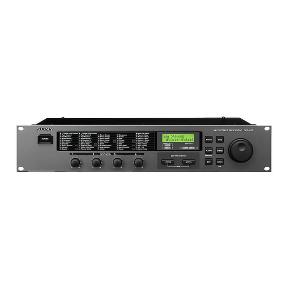
- Page 1 DPS-V55/V55M SERVICE MANUAL US Model Canadian Model DPS-V55 AEP Model UK Model DPS-V55M Photo: DSP-V55 SPECIFICATIONS MULTI-EFFECT PROCESSOR MICROFILM...
-
Page 2: Table Of Contents
OPERATION. REPLACE THESE COMPONENTS WITH DE FONCTIONNEMENT. NE REMPLACER CES COM- SONY PARTS WHOSE PART NUMBERS APPEAR AS POSANTS QUE PAR DES PIÈCES SONY DONT LES SHOWN IN THIS MANUAL OR IN SUPPLEMENTS PUB- NUMÉROS SONT DONNÉS DANS CE MANUEL OU LISHED BY SONY. -
Page 3: Servicing Notes
SECTION 1 SERVICING NOTES ROM VERSION CHECK Flexible Circuit Board Repairing • This system have ROM version check function consequently key • Keep the temperature of the soldering iron around 270 ˚C during set up of when power on. repairing. (No need in open the main body) •... - Page 4 SAFETY CHECK-OUT After correcting the original service problem, perform the follow- ing safety check before releasing the set to the customer: Check the antenna terminals, metal trim, “metallized” knobs, screws, and all other exposed metal parts for AC leakage. Check leakage as described below. LEAKAGE TEST The AC leakage from any exposed metal part to earth ground and from all exposed metal parts to any exposed metal part having a...
-
Page 5: General
SECTION 2 This section is extracted from instruction manual. GENERAL – 5 –... - Page 6 – 6 –...
- Page 7 – 7 –...
- Page 8 – 8 –...
-
Page 9: Disassembly
SECTION 3 DISASSEMBLY Note: Follow the disassembly procedure in the numerical order given. CASE 1 two screws (case 3 TP2) 1 three screws 2 two screws (case 3 TP2) (case 3 TP2) 3 case 2 two screws (case 3 TP2) FRONT PANEL ASS’Y 4 clamp 5 front panel ass’y... - Page 10 BACK PANEL 3 screw (BVTT3 × 6) 2 six screws (BVTP3 × 10) 1 connector (CN601) 2 four lock screws 3 three screws (BVTT3 × 6) 3 screw (BVTT3 × 6) 4 back panel MAIN BOARD 1 connector (CN101) 1 connector 1 connector (CN602) 2 two screws...
-
Page 11: Test Mode
SECTION 4 TEST MODE [Operation of Test Mode] 4 Signal check 1 (Bypass check mode) 1) Press n button. • The test mode is executed according to order the following. 2) Enter the bypass check mode. • Press N button, and come back the before item. Analog output muting is OFF, and each channel the out- put signal as intact as input signal. - Page 12 [Self-diagnosis Display] [Initialize Method] [SAVE] [SYSTEM] [POWER] Press three buttons , and (1) ROM Error multaneously, and the display of fluorescent indicator tube Contents: Data of EPROM (IC704) is wrong. changes to “All Initialize!!”, and restart system. Method: • Check the bridge is possible and if find out a repair.
-
Page 13: Diagrams
DPS-V55/V55M SECTION 5 DIAGRAMS • Circuit Boards Location THIS NOTE IS COMMON FOR PRINTED WIRING BOARDS AND SCHEMATIC DIAGRAMS. (In addition to this, the necessary note is each block.) POWER SWITCH board Note on Schematic Diagram: • Signal path. • All capacitors are in µF unless otherwise noted. pF: µµF... -
Page 14: Printed Wiring Board - Main Section
DPS-V55/V55M 5-1. PRINTED WIRING BOARD – MAIN Section – • See page 13 for Circuit Boards Location. • See page 14 for Note on Printed Wiring Board. (Page 23) (Page 23) (Page 24) (Page 23) (Page 23) (Page 23) – 15 –... -
Page 15: Schematic Diagram - Main Section (1/3)
DPS-V55/V55M • Semiconductor 5-2. SCHEMATIC DIAGRAM – MAIN Section (1/3) – Location • See page 14 for Note on Schematic Diagram and IC Block Diagrams. • See page 27 for Waveforms. Ref. No. Location D101 E-10 D102 E-10 D103 E-10... -
Page 16: Schematic Diagram - Main Section (2/3)
DPS-V55/V55M 5-3. SCHEMATIC DIAGRAM – MAIN Section (2/3) – • See page 14 for Note on Schematic Diagram and IC Block Diagrams. • See pages 15 and 16 for Printed Wiring Board. • See page 27 for Waveforms. (Page 18) (Page 21) –... -
Page 17: Schematic Diagram - Main Section (3/3)
DPS-V55/V55M The components identified by mark ! or dotted Les composants identifiés par une marque ! sont 5-4. SCHEMATIC DIAGRAM – MAIN Section (3/3) – line with mark ! are critical for safety. critiques pour la sécurité. Ne les remplacer que •... -
Page 18: Printed Wiring Boards - Panel Section
DPS-V55/V55M 5-5. PRINTED WIRING BOARDS – PANEL Section – • See page 13 for Circuit Boards Location. • See page 14 for Note on Printed Wiring Boards. (Page 15) (Page 16) SW841 (OPERATION DIAL) (Page 15) (Page 16) (Page 16) -
Page 19: Schematic Diagram - Panel Section
DPS-V55/V55M 5-6. SCHEMATIC DIAGRAM – PANEL Section – • See page 14 for Note on Schematic Diagram. (Page 17) (Page 17) (Page 22) (Page 17) (Page 17) (Page 17) The components identified by mark ! or dotted Les composants identifiés par une marque ! sont line with mark ! are critical for safety. -
Page 20: Ic Pin Function Description
DPS-V55/V55M • Waveforms 5-7. IC PIN FUNCTION DESCRIPTION – MAIN BOARD – • MAIN BOARD IC502 CXD2707Q (DSP) 1 IC501 3 (MCLK) , IC5513 (MCLK) !¡ IC701 *™ (X0) 6 IC502 @¡ (BCKO) Pin No. Pin Name Function Address signal output to the external RAM device Not used (open) Address signal output to the memory (IC503) 3.8 Vp-p... - Page 21 Pin No. Pin Name Function ED16 Two-way data bus with the memory (IC503) Two-way data bus with the external RAM device Not used ED17 Two-way data bus with the memory (IC503) Two-way data bus with the external RAM device Not used —...
- Page 22 • MAIN BOARD IC701 MB90641APF-G-105BND (CPU) Pin No. Pin Name Function 1 to 10 A0 to A9 Address signal output to the static RAM (IC702) and EP-ROM (IC704) — Ground terminal 12 to 16 A10 to A14 Address signal output to the static RAM (IC702) and EP-ROM (IC704) 17, 18 A15, A16 Address signal output to the EP-ROM (IC704)
- Page 23 Pin No. Pin Name Function Register selection signal output to the LCD module (LCD801) Data read/write selection signal output to the LCD module (LCD801) Enable signal output to the LCD module (LCD801) — Not used (open) RSTX Reset signal input terminal “L”: reset Write strobe signal output to the static RAM (IC702) Read strobe signal output to the static RAM (IC702) and EP-ROM (IC704) —...
-
Page 24: Exploded Views
4-997-525-01 WINDOW (LED), INDICATION 1-773-178-11 WIRE (FLAT TYPE) (23 CORE) 4-997-524-01 WINDOW (LCD), INDICATION 4-988-161-01 SPRING, RING 4-908-848-31 EMBLEM, SONY 3-363-099-21 SCREW (CASE 3 TP2) 4-997-528-01 PANEL, FRONT (DPS-V55) * 12 4-997-712-01 CASE 4-997-528-11 PANEL, FRONT (DPS-V55M) * 13 1-668-986-11 ENCODER BOARD... - Page 25 * 64 1-668-988-11 JACK BOARD (DPS-V55M) ! 57 1-575-651-21 CORD, POWER (DPS-V55M) * 65 4-999-176-01 CUSION (DIA.10) ! 57 1-590-836-11 CORD, POWER (DPS-V55) ! T601 1-431-768-11 TRANSFORMER, POWER (DPS-V55M) 3-703-244-00 BUSHING (2104), CORD ! T601 1-431-769-11 TRANSFORMER, POWER (DPS-V55) * 59 4-997-529-11 PANEL, BACK (DPS-V55) –...
- Page 26 ENCODER JACK SECTION 7 ELECTRICAL PARTS LIST NOTE: • Due to standardization, replacements in the • Items marked “*” are not stocked since they The components identified by mark ! or dotted line with mark parts list may be different from the parts speci- are seldom required for routine service.
- Page 27 MAIN Ref. No. Part No. Description Remark Ref. No. Part No. Description Remark S825 1-554-303-21 SWITCH, TACTILE (EXIT) C312 1-110-339-11 MYLAR 220PF C313 1-130-475-00 MYLAR 0.0022uF 5% S826 1-554-303-21 SWITCH, TACTILE (ENTER TAP) C314 1-126-022-11 ELECT 47uF S827 1-554-303-21 SWITCH, TACTILE (EDIT PARAMETER SKIP ∫) S828 1-554-303-21 SWITCH, TACTILE (EDIT PARAMETER SKIP ı) C315...
- Page 28 MAIN Ref. No. Part No. Description Remark Ref. No. Part No. Description Remark C606 1-136-165-00 FILM 0.1uF CN703 1-506-468-11 PIN, CONNECTOR 3P C607 1-136-165-00 FILM 0.1uF C608 1-136-165-00 FILM 0.1uF < DIODE > C609 1-136-165-00 FILM 0.1uF C610 1-136-165-00 FILM 0.1uF D101 8-719-911-19 DIODE 1SS119...
- Page 29 MAIN Ref. No. Part No. Description Remark Ref. No. Part No. Description Remark IC402 8-759-711-82 IC NJM4580E L701 1-410-521-11 INDUCTOR 100uH IC403 8-759-711-82 IC NJM4580E L702 1-410-521-11 INDUCTOR 100uH IC501 8-759-530-36 IC CS4222-KS L703 1-410-521-11 INDUCTOR 100uH L704 1-410-521-11 INDUCTOR 100uH IC502 8-752-362-00 IC CXD2707Q...
- Page 30 MAIN Ref. No. Part No. Description Remark Ref. No. Part No. Description Remark R129 1-216-178-00 RES,CHIP 1/8W R323 1-216-210-00 RES,CHIP 3.3K 1/8W R130 1-216-178-00 RES,CHIP 1/8W R324 1-208-494-61 RES,CHIP 2.2K 1/8W R131 1-208-510-61 RES,CHIP 1/8W R325 1-208-484-11 RES,CHIP 1/8W R326 1-216-202-00 RES,CHIP 1.5K 1/8W...
- Page 31 R722 1-216-129-00 METAL CHIP 2.2M 1/10W C901 1-136-153-00 FILM 0.01uF (DPS-V55) The components identified by Les composants identifiés par une mark ! or dotted line with marque ! sont critiques pour la mark ! are critical for safety. sécurité. Replace only with part num- Ne les remplacer que par une pièce...
- Page 32 * CN351 1-564-521-11 PLUG, CONNECTOR 6P ! 57 1-575-651-21 CORD, POWER (DPS-V55M) CN901 1-766-798-11 CONNECTOR, BOARD TO BOARD 5P ! 57 1-590-836-11 CORD, POWER (DPS-V55) (DPS-V55M) ! T601 1-431-768-11 TRANSFORMER, POWER (DPS-V55M) < DIODE > ! T601 1-431-769-11 TRANSFORMER, POWER (DPS-V55)
Need help?
Do you have a question about the DPS-V55 and is the answer not in the manual?
Questions and answers