Table of Contents
Advertisement
Quick Links
Is Now Part of
To learn more about ON Semiconductor, please visit our website at
www.onsemi.com
ON Semiconductor and the ON Semiconductor logo are trademarks of Semiconductor Components Industries, LLC dba ON Semiconductor or its subsidiaries in the United States and/or other countries. ON Semiconductor owns the rights to a number
of patents, trademarks, copyrights, trade secrets, and other intellectual property. A listing of ON Semiconductor's product/patent coverage may be accessed at www.onsemi.com/site/pdf/Patent-Marking.pdf. ON Semiconductor reserves the right
to make changes without further notice to any products herein. ON Semiconductor makes no warranty, representation or guarantee regarding the suitability of its products for any particular purpose, nor does ON Semiconductor assume any liability
arising out of the application or use of any product or circuit, and specifically disclaims any and all liability, including without limitation special, consequential or incidental damages. Buyer is responsible for its products and applications using ON
Semiconductor products, including compliance with all laws, regulations and safety requirements or standards, regardless of any support or applications information provided by ON Semiconductor. "Typical" parameters which may be provided in ON
Semiconductor data sheets and/or specifications can and do vary in different applications and actual performance may vary over time. All operating parameters, including "Typicals" must be validated for each customer application by customer's
technical experts. ON Semiconductor does not convey any license under its patent rights nor the rights of others. ON Semiconductor products are not designed, intended, or authorized for use as a critical component in life support systems or any FDA
Class 3 medical devices or medical devices with a same or similar classification in a foreign jurisdiction or any devices intended for implantation in the human body. Should Buyer purchase or use ON Semiconductor products for any such unintended
or unauthorized application, Buyer shall indemnify and hold ON Semiconductor and its officers, employees, subsidiaries, affiliates, and distributors harmless against all claims, costs, damages, and expenses, and reasonable attorney fees arising out
of, directly or indirectly, any claim of personal injury or death associated with such unintended or unauthorized use, even if such claim alleges that ON Semiconductor was negligent regarding the design or manufacture of the part. ON Semiconductor
is an Equal Opportunity/Affirmative Action Employer. This literature is subject to all applicable copyright laws and is not for resale in any manner.
Advertisement
Table of Contents

Subscribe to Our Youtube Channel
Related Manuals for Fairchild FEBFAN9611 S01U300A


Summary of Contents for Fairchild FEBFAN9611 S01U300A
- Page 1 Is Now Part of To learn more about ON Semiconductor, please visit our website at www.onsemi.com ON Semiconductor and the ON Semiconductor logo are trademarks of Semiconductor Components Industries, LLC dba ON Semiconductor or its subsidiaries in the United States and/or other countries. ON Semiconductor owns the rights to a number of patents, trademarks, copyrights, trade secrets, and other intellectual property.
-
Page 2: Evaluation Board
User Guide for FEBFAN9611_S01U300A Evaluation Board FAN9611 300W Interleaved Dual-BCM, Low-Profile, PFC Evaluation Board Featured Fairchild Product: FAN9611 Direct questions or comments about this evaluation board to: “Worldwide Direct Support” Fairchild Semiconductor.com © 2012 Fairchild Semiconductor Corporation FEBFAN9611_S01U300A • Rev. 0.0.1... -
Page 3: Table Of Contents
10.8. Harmonic Distortion and Power Factor ................32 10.9. EMI ..........................33 References ..........................34 Ordering Information ......................34 Revision History ........................34 © 2012 Fairchild Semiconductor Corporation FEBFAN9611_S01U300A • Rev. 0.0.1... -
Page 4: Overview Of The Evaluation Board
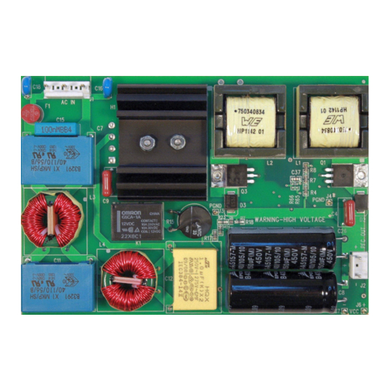
The following user guide supports the FAN9611 300W evaluation board for interleaved boundary-conduction-mode power-factor-corrected supply. It should be used in conjunction with the FAN9611 datasheet, Fairchild application note AN-6086 —Design Considerations for Interleaved Boundary-Conduction Mode PFC Using FAN9611 / and FAN9611/12 PFC Excel®-based Design Tool. - Page 5 Figure 1. FEBFAN9611_S01U300A, Top View, 152mm x 105mm Figure 2. FEBFAN9611_S01U300A, Side View (Low Profile), Cross Section=18mm Figure 3. FEBFAN9611_S01U300A, Bottom View, 152mm x 105mm © 2012 Fairchild Semiconductor Corporation FEBFAN9611_S01U300A • Rev. 0.0.1...
-
Page 6: Key Features
K1 V AGND DRV2 5µA PGND INPUT VOLTAGE SENSE COMP (Input Voltage Squarer, Input UVLO, Brownout) Phase Management 2µA PROTECTION LOGIC (Open FB, Brownout Protection, OVP, Latched OVP) Figure 4. Block Diagram © 2012 Fairchild Semiconductor Corporation FEBFAN9611_S01U300A • Rev. 0.0.1... -
Page 7: Specifications
AC line current remains sinusoidal. The phase-management function permits phase shedding / adding ~18% of the nominal output power for high line (230V ). This level can be increased by modifying the MOT resistor (R6) as described in Fairchild Application Note AN-6086 —Design Considerations for Interleaved Boundary- Conduction Mode PFC Using FAN9611 / FAN9612. -
Page 8: Test Procedure
AC input voltage is greater than 90V 3. Change load current (0~0.75A) and check the operation 4. Verify the output voltage is regulating between 395V <V <405V © 2012 Fairchild Semiconductor Corporation FEBFAN9611_S01U300A • Rev. 0.0.1... - Page 9 3. Disconnect (shut down) 12V DC bias power supply. 4. Disconnect (shut down) DC electronic load last to ensure that the output capacitors are fully discharged before handling the evaluation module. © 2012 Fairchild Semiconductor Corporation FEBFAN9611_S01U300A • Rev. 0.0.1...
-
Page 10: Schematic
5. Schematic Figure 6. FEBFAN9611_S01U300A 300W Evaluation Board Schematic © 2012 Fairchild Semiconductor Corporation FEBFAN9611_S01U300A • Rev. 0.0.1... -
Page 11: Boost Inductor Specification
Figure 7. Boost Inductor (L1, L2) in the Evaluation Board Figure 8. Wurth 750340834 Mechanical Drawing Table 3. Inductor Turns Specifications Turns Wire 1 6 69 (3 Layers) 30xAWG#38 Litz BOOST Insulation Tape 10 9 AWG#28 Insulation Tape © 2012 Fairchild Semiconductor Corporation FEBFAN9611_S01U300A • Rev. 0.0.1... -
Page 12: Four-Layer Pcb And Assembly Images
7. Four-Layer PCB and Assembly Images Figure 9. Layer 1 – Top Layer Figure 10. Layer 2 – Internal Layer © 2012 Fairchild Semiconductor Corporation FEBFAN9611_S01U300A • Rev. 0.0.1... - Page 13 Figure 11. Layer 3 – Internal Layer Figure 12. Layer 4 – Bottom Layer © 2012 Fairchild Semiconductor Corporation FEBFAN9611_S01U300A • Rev. 0.0.1...
- Page 14 Figure 13. Top Assembly Figure 14. Bottom Assembly © 2012 Fairchild Semiconductor Corporation FEBFAN9611_S01U300A • Rev. 0.0.1...
-
Page 15: Bill Of Materials (Bom)
750340834/NP1138-01 280µH Inductor, Coupled Wurth Thru-Hole L3-4 750311795 Common Mode Choke, 9mH Wurth Thru-Hole MOSFET, NCH, UniFET, Fairchild Q1, Q3 FDP22N50N TO-220 500V, 11.5A, 0.18Ω Semiconductor Continued on the following page… © 2012 Fairchild Semiconductor Corporation FEBFAN9611_S01U300A • Rev. 0.0.1... - Page 16 N1, N2 HNZ440 NUT HEX 4-40 ZINC PLATED Hardware 4 Layer, FR4, FAN9611 LOW- Fairchild PROFILE PWB - REV. 1.0 Semiconductor Notes: DNP = Do Not Populate STD = Standard Components © 2012 Fairchild Semiconductor Corporation FEBFAN9611_S01U300A • Rev. 0.0.1...
-
Page 17: Inrush Current Limiting
R16 PCB pad locations. A current probe can then be connected to the wire loop. The effectiveness of the inrush current limiting function is shown below in Figure 16. © 2012 Fairchild Semiconductor Corporation FEBFAN9611_S01U300A • Rev. 0.0.1... - Page 18 % Inrush Input Line Output Peak Line Current Peak Line Current Current Voltage Power (Inrush Circuit Disabled) (Inrush Circuit Enabled) Reduction =115V 300W 22.50A 8.45A 62.40% =230V 300W 26.9A 11.5A 57.3% © 2012 Fairchild Semiconductor Corporation FEBFAN9611_S01U300A • Rev. 0.0.1...
-
Page 19: Test Results
Figure 17. No-Load Startup at 115V DRV1 COMP Line Current CH1: Gate Drive 1 Voltage (20V/div), CH2: COMP Voltage (2V/div), CH3: Output Voltage (200V/div), CH4: Line Current (5A/div), Time (200ms/div) Figure 18. Full-Load Startup at 115V © 2012 Fairchild Semiconductor Corporation FEBFAN9611_S01U300A • Rev. 0.0.1... - Page 20 Figure 19. No-Load Startup at 230V DRV1 COMP Line Current CH1: Gate Drive 1 Voltage (20V/div), CH2: COMP Voltage (2V/div), CH3: Output Voltage (200V/div), CH4: Line Current (10A/div), Time (100ms/div) Figure 20. Full-Load Startup at 230V © 2012 Fairchild Semiconductor Corporation FEBFAN9611_S01U300A • Rev. 0.0.1...
-
Page 21: Steady State Operation
Figure 21. Zoom of Inductor Current Waveforms at Full-Load and 90V CH3: Inductor L1 Current (2A/div), CH4: Inductor L2 Current (2A/div), CH2: Sum of Two Inductor Current (2A/div), Time (2ms/div) Figure 22. Zoom of Inductor Current Waveforms at Full-Load and 230V © 2012 Fairchild Semiconductor Corporation FEBFAN9611_S01U300A • Rev. 0.0.1... - Page 22 Figure 23. Zero Valley Switching at Full Load, 115V DS(Q3) DRV1 ZCD1 CH1: DRV1 (20V/div), CH2: VDS(Q3) (100V/div) CH3: ZCD1 (1V/div), CH4: Inductor L2 Current (5A/div) Figure 24. Zero Valley Switching at Full Load, 230V © 2012 Fairchild Semiconductor Corporation FEBFAN9611_S01U300A • Rev. 0.0.1...
- Page 23 Figure 25. Zoom of Valley Switching at Full Load, 230V CH1: FAN9611, Pin 16 (100mV/div), CH2: FAN9611, Pin 15 (100mV/div) CH3: Inductor L2 Current (5A/div), CH4: Inductor L1 Current (5A/div) Figure 26. Current-Sense Waveforms at Full Load, 90V © 2012 Fairchild Semiconductor Corporation FEBFAN9611_S01U300A • Rev. 0.0.1...
- Page 24 CH1: Inductor L1 Current (5A/div), CH2: Inductor L2 Current (5A/div) CH3: Output Voltage (100V/div), CH4: Line Current (5A/div), Time (20ms/div) Figure 28. MOT Power Limit, 0.5A to 1.3A Load Transient, 115V © 2012 Fairchild Semiconductor Corporation FEBFAN9611_S01U300A • Rev. 0.0.1...
-
Page 25: Line Transient
Current CH1: Rectified Line Voltage (200V/div), CH2: Output Voltage (10V/div, AC), CH3: COMP Voltage (2V/div), CH4: Line Current (5A/div), Time (50ms/div) 230V Figure 30. Line Transient Response at Full-Load Condition (115V © 2012 Fairchild Semiconductor Corporation FEBFAN9611_S01U300A • Rev. 0.0.1... -
Page 26: Load Transient
CH1: Rectified Line Voltage (100V/div), CH2: Output Voltage (20V/div, AC), CH3: COMP Voltage (2V/div), CH4: Line Current (5A/div), Time (50ms/div) (No Load Full Load) Figure 32. Load Transient Response at 115V © 2012 Fairchild Semiconductor Corporation FEBFAN9611_S01U300A • Rev. 0.0.1... - Page 27 CH1: Rectified Line Voltage (100V/div), CH2: Output Voltage (20V/div, AC), CH3: COMP Voltage (5V/div), CH4: Line Current (5A/div), Time (50ms/div) (No Load Full Load) Figure 34. Load Transient Response at 230V © 2012 Fairchild Semiconductor Corporation FEBFAN9611_S01U300A • Rev. 0.0.1...
-
Page 28: Brownout Protection
Figure 35. Startup Slowly Increasing the Line Voltage Line Voltage DRV1 Line Current CH1: Line Voltage (100V/div), CH2: Gate Drive 1 Voltage (10V/div), CH4: Line Current (5A/div), Time (20ms/div) Figure 36. Shutdown Slowly Decreasing the Line Voltage © 2012 Fairchild Semiconductor Corporation FEBFAN9611_S01U300A • Rev. 0.0.1... -
Page 29: Phase Management
DRV2 CH1: Gate Drive 1 Voltage (20V/div), CH2: Gate Drive 2 Voltage (20V/div), CH3: Inductor L1 Current (1A/div), CH4: Inductor L2 Current (1A/div), Time (5µs/div) Figure 38. Phase-Shedding Operation (Zoomed-in Timescale) © 2012 Fairchild Semiconductor Corporation FEBFAN9611_S01U300A • Rev. 0.0.1... - Page 30 DRV2 CH1: Gate Drive 1 Voltage (20V/div), CH2: Gate Drive 2 Voltage (20V/div), CH3: Inductor L1 Current (1A/div), CH4: Inductor L2 Current (1A/div), Time (5µs/div) Figure 40. Phase-Adding Operation (Zoomed-in Timescale) © 2012 Fairchild Semiconductor Corporation FEBFAN9611_S01U300A • Rev. 0.0.1...
-
Page 31: Efficiency
Figure 42. Efficiency vs. Load (230V Efficiency vs. Load Efficiency vs. Load (115V , 400V Output, R =120KΩ, No Inrush Circuit) (230V , 400V Output, R =120KΩ, No Inrush Circuit) 100% 100% 100% 100% Output Power (%) Output Power (%) Figure 43. Efficiency vs. Load (115V Figure 44. Efficiency vs. Load (230V © 2012 Fairchild Semiconductor Corporation FEBFAN9611_S01U300A • Rev. 0.0.1... - Page 32 120kΩ, the maximum allowable output power is also increased to greater than 400W. To fully protect the power stage, a simple voltage divider and PNP clamp should be applied to the FAN9611 COMP voltage (pin 7) as detailed in AN-6086, Figure 15. © 2012 Fairchild Semiconductor Corporation FEBFAN9611_S01U300A • Rev. 0.0.1...
-
Page 33: Harmonic Distortion And Power Factor
230V . As observed, high power factor above 0.95 is obtained from 100% to 50% load. Figure 50 shows the total harmonic distortion at input voltages of 115V and 230V © 2012 Fairchild Semiconductor Corporation FEBFAN9611_S01U300A • Rev. 0.0.1... -
Page 34: Emi
1 PK MAXH MAXH 2 AV 2 AV MAXH MAXH EN55022Q EN55022Q EN55022A EN55022A 150 kHz 30 MHz 150 kHz 30 MHz Figure 53. 230 , Line Figure 54. 230V , Neutral © 2012 Fairchild Semiconductor Corporation FEBFAN9611_S01U300A • Rev. 0.0.1... -
Page 35: References
Fairchild warrantees that its products meet Fairchild’s published specifications, but does not guarantee that its products work in any specific application. Fairchild reserves the right to make changes without notice to any products described herein to improve reliability, function, or design. - Page 36 ON Semiconductor and are trademarks of Semiconductor Components Industries, LLC dba ON Semiconductor or its subsidiaries in the United States and/or other countries. ON Semiconductor owns the rights to a number of patents, trademarks, copyrights, trade secrets, and other intellectual property. A listing of ON Semiconductor’s product/patent coverage may be accessed at www.onsemi.com/site/pdf/Patent−Marking.pdf.
Need help?
Do you have a question about the FEBFAN9611 S01U300A and is the answer not in the manual?
Questions and answers