Table of Contents
Advertisement
SERVICE MANUAL
I CONTENTS
PANEL LAYOUT .......................................................................................... 3
CIRCUIT BOARD LAYOUT ......................................................................... 4
SERVICE PRECAUTIONS ........................................................................... 5
OVERALL ASSEMBLY WIRING .................................................................. 7
DISASSEMBLY PROCEDURES ................................................................ 17
LSI PIN DESCRIPTION .............................................................................. 26
IC BLOCK DIAGRAM ................................................................................ 27
CIRCUIT BOARDS ..................................................................................... 33
TEST PROGRAM ....................................................................................... 52
INSPECTIONS ........................................................................................... 59
UPDATING THE FIRMWARE .................................................................... 64
PARTS LIST
IC & DIODE FIGURES
BLOCK DIAGRAM
CIRCUIT DIAGRAM
Copyright (c) NEXO S.A. All rights reserved. PDF ' 08.01
Advertisement
Chapters
Table of Contents

Related Manuals for Nexo NXAMP4x1


Summary of Contents for Nexo NXAMP4x1
- Page 1 IC BLOCK DIAGRAM ................27 CIRCUIT BOARDS ..................33 TEST PROGRAM ..................52 INSPECTIONS ................... 59 UPDATING THE FIRMWARE ..............64 PARTS LIST IC & DIODE FIGURES BLOCK DIAGRAM CIRCUIT DIAGRAM Copyright (c) NEXO S.A. All rights reserved. PDF ’ 08.01...
- Page 2 NXAMP4x1 WARNING: This product contains chemicals known to the State of California to cause cancer, or birth defects or other reproductive harm. DO NOT PLACE SOLDER, ELECTRICAL/ELECTRONIC OR PLASTIC COMPONENTS IN YOUR MOUTH FOR ANY REASON WHAT SO EVER! Avoid prolonged, unprotected contact between solder and your skin! When soldering, do not inhale solder fumes or expose eyes to solder/flux vapor! If you come in contact with solder or components located inside the enclosure of this product, wash your hands before handling food.
-
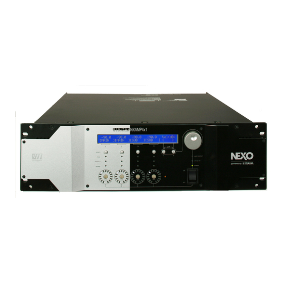
Page 3: Panel Layout
NXAMP4x1 PANEL LAYOUT • Front Panel 1 Power switch 7 Mute buttons 2 Amplifier indicators 8 Select buttons 3 LCD display 9 Channel indicators 4 Encoder 0 Air intakes 5 Navigation buttons (A & B) A Screw holes for handles 6 Volume indicators •... -
Page 4: Circuit Board Layout
NXAMP4x1 CIRCUIT BOARD LAYOUT RS232-GPI INANL OPT-AN OUTANL PAANL PAANL (PA unit) (PA unit) CONTROL PSANL Rear Panel OUTANL RS232-GPI OPT-AN INANL PSANL Front Panel PAANL PAANL PN-AN (PA unit) (PA unit) -
Page 5: Service Precautions
NXAMP4x1 SERVICE PRECAUTIONS Safety measures • Some component parts on the PSANH circuit board main- [Discharging Method] tain a high voltage even when the power is switched off. Before starting the service work, connect discharging For this reason to avoid an electrical shock, do not touch... - Page 6 NXAMP4x1 PSANL circuit diagram 220 ohms/10W C205 C205 C201 C201 220 ohms/10W 220 ohms/10W C305 C305 C316 C316 C322 C344 C344 C354 C354 C316 C316 D305 D305 C345 C345 C355 C355 C307 C307 220 ohms/10W C317 C323 220 ohms/10W 5...
-
Page 7: Overall Assembly Wiring
NXAMP4x1 OVERALL ASSEMBLY WIRING This product has various cables (wires and connector assemblies) inside. To prevent touching component to the cables and/ or connection mistake, perform the cable connection and fixing cables according to the following instructions referring the wiring diagram, P3 of the circuit diagram. -
Page 8: Connect The Connector Of The Fan To The Each Terminal. (Fig
NXAMP4x1 Confirm that the power switch is set to the off position as shown in the figure 6. (Fig. 6) Twist the wires of the power switch assembly more than three times. Connect the connector of the power switch assembly to the connector (CN103). (Fig. 7) - Page 9 NXAMP4x1 5. Wiring of the AC-INLET Set a cord holder before installing the PSAN circuit board Set a ferrite-core at the specified area on the PSAN cir- on the enclosure. (Fig. 10) cuit board, and fasten the ferrite-core with the cord holder.
- Page 10 NXAMP4x1 6. Wiring of the PA-UNIT Connect the wires to the connectors (CN401, CN403). (Fig. 16, 17) CN403 CN401 CN403 CN401 BLUE GREEN YELLOW Fig. 16 Fig. 17 NOTE: The followings are wires to be connected. NOTE: The followings are wires to be connected.
- Page 11 NXAMP4x1 Connect the wire (WK14210) of PA-UNIT (CH1, CH2) to the connector (CN312). Fasten the wire (WK14210) and the wire (WK02090) with a cord holder at the position where the wire (WK14210) is vertically pulled from PA-UNIT. Before fastening, pull the wire (WK02090) toward the front panel side in advance.
- Page 12 NXAMP4x1 Fasten these wires (WK17900, WK17910 and WK94710) with a cord holder to the hexagonal spacer. (Fig. 21) Bend the wire (WK14200) and wire (WK16820) connected to the connector (CN317), and fasten the wires (WK14210, WK16820 x 2 and WK14200) with a cord holder. (Fig. 21) Fig.
- Page 13 NXAMP4x1 The hole of the enclosure The hole of the enclosure Fig. 22...
- Page 14 NXAMP4x1 Bend the flat cable to avoid touching the top cover. (Fig. 23, 24) Fig. 23 Fig. 24 8. Color of the connectors connected to the connector CN012-CN015 Connect the connector assembly from the PA unit to the CONTROL circuit board as shown in the figure below. (Fig. 25)
- Page 15 NXAMP4x1 10. Insulation distance between WK17110 and primary side capacitor Perform wiring the connector assembly WK17110 with care so that its uncovered portion with the SUMI tube does not touch the capacitor C316 on primary side of the PSANL circuit board. (Fig. 28, 29) Fig.
- Page 16 NXAMP4x1 12. Prevention of touching WK02070 to connector terminal Perform wiring the connector assembly WK02070 with care so that its uncovered portion with the SUMI tube does not touch the bare terminal of the connector CN203 of the RS232-GPI circuit board. (Fig. 32)
-
Page 17: Disassembly Procedures
NXAMP4x1 DISASSEMBLY PROCEDURES Top Cover (Time required: about 3 minutes) 1-1. Remove the thirteen (13) screws marked [650]. (Fig. 1) 1-2. The top cover can then be removed. (Fig. 1) [650] [650] [650] Top cover Top cover Top cover [650]... - Page 18 NXAMP4x1 CONTROL Circuit Board, OPT angle and OPT-AN Circuit Board (Time required: about 10 minutes) 2-1. Remove the top cover. (See procedure 1.) 2-2. Remove the four (4) screws marked [430]. (Fig. 2) 2-3. Disconnect the connector assemblies from other units connected to the CONTROL circuit board. (Fig. 2) 2-4.
- Page 19 NXAMP4x1 OUTANL Circuit Board (Time required: about 15 minutes) 3-1. Remove the top cover. (See procedure 1.) 3-2. Remove the CONTROL circuit board and the OPT angle. (See procedure 2.) 3-3. Remove the eight (8) screws marked [280], the one (1) screw marked [290] and the one (1) screw marked [285]. (Fig. 3) 3-4.
- Page 20 NXAMP4x1 PSANL Circuit Board (Time required: about 20 minutes) 4-1. Remove the top cover. (See procedure 1.) 4-2. Remove the CONTROL circuit Board and the OPT angle. (See procedure 2.) 4-3. Remove the OUTANL Circuit Board. (See procedure 3.) 4-5.
- Page 21 NXAMP4x1 INANL Circuit Board RS232-GPI Circuit Board (Time required: about 7 minutes) (Time required: about 7 minutes) 5-1. Remove the top cover. (See procedure 1.) 6-1. Remove the top cover. (See procedure 1.) 5-2. Remove the sixteen (16) screws marked [70]. (Fig. 5) 6-2.
- Page 22 NXAMP4x1 Left (CH1, CH2) PA unit Right (CH3, CH4) PA unit (Time required: about 15 minutes) (Time required: about 15 minutes) 7-1. Remove the top cover. (See procedure 1.) 8-1. Remove the top cover. (See procedure 1.) 7-2. Remove the CONTROL circuit board and the OPT 8-2.
- Page 23 NXAMP4x1 Front Panel Assembly PN-AN Circuit Board (Time required: about 6 minutes) (Time required: about 10 minutes) 9-1. Remove the top cover. (See procedure 1.) 10-1. Remove the top cover. (See procedure 1.) 9-2. Remove the CONTROL circuit Board and the OPT 10-2.
- Page 24 NXAMP4x1 Left DC Fan (Time required: about 15 minutes) Right DC fan (Time required: about 15 minutes) 11-1. Remove the top cover. (See procedure 1.) 12-1. Remove the top cover. (See procedure 1.) 11-2. Remove the CONTROL circuit board and the OPT 12-2.
- Page 25 NXAMP4x1 Power switch (Time required: about 15 minutes) 13-1. Remove the top cover. (See procedure 1.) 13-2. Remove the CONTROL circuit Board and the OPT angle. (See procedure 2.) 13-3. Disconnect the connector of the power switch assembly connected to the PSANL circuit board. (Fig. 9) 13-4.
-
Page 26: Lsi Pin Description
NXAMP4x1 LSI PIN DESCRIPTION • PCM1803ADBR (X7357B0) A/D CONVERTER CONTROL: IC035, IC036, IC037, IC038 NAME FUNCTION Analog input, L-channel Analog input, R-channel – Reference voltage 1 decoupling capacitor – Reference voltage 2 decoupling capacitor – Analog power supply, 5 V AGND –... -
Page 27: Ic Block Diagram
NXAMP4x1 IC BLOCK DIAGRAM • 74HCT273PW,118 (X8681A0) • 74LVC169PW,118 (X8482A0) D-type Flip Flop Binaly Counter PN-AN: IC002, 003 CONTROL: IC044, 045 • 74HCT4514PW,118 (X8630A0) • CS3318-CQZ (X8486A0) Decoder Volume Controller PN-AN: IC004-007 CONTROL: IC001 REFI1 RESET OUT5 V CC latch... - Page 28 NXAMP4x1 • CS4272-CZZR (X8487A0) • DSPB56371AF180 (X8489A0) CODEC CONTROL: IC012, 013 CONTROL: IC022, 023 2.5V to 5V 3.3V to 5V Memory Expansion Area Hardware or Left and Internal Voltage Internal External I2C/SPI Right Mute Triple ESAI ESAI_1 GPIO EFCOP Reference...
- Page 29 NXAMP4x1 • MX25L1605AM2C-12G (X8718A0) • NJM431U (TE1) (X6770A0) Flash Memory SHUNT Regulator CONTROL: IC039 PSANL: IC204 CATHOD HOLD# REFERENCE SCLK Address Generator Memory Array Page Buffer ANODE Data Register REFERENCE (R) Y-Decoder ANODE CATHODE SRAM Buffer Output Sense Buffer Amplifire...
- Page 30 NXAMP4x1 • NJU7630-M (X8682A0) • PCM1803ADBR (X7357B0) Regulator A/D Converter PSANL: IC205 CONTROL: IC035-038 MODE1 MODE0 FMT1 FMT0 ER.AMP 0.8V AGND SCKI 0.2V PDWN Vref BYPAS DGND TEST DOUT Soft Start LRCK UVLO Latch Delta-Sigma Modulator Buffer LRCK 2µA DOUT...
- Page 31 NXAMP4x1 • SN74ABT245BNSR (XU009A0) • SN74LV14APWR (X6688A0) BUS Transceiver Inverter CONTROL: IC062 CONTROL: IC063 • SN74LV273APWR (X5074A0) • SN74LV541APWRBUS B (X5966A0) D-type Flip Flop Buffer/Driver CONTROL: IC057-061 CONTROL: IC055, 056 PN-AN: IC001 • SN74LV4052APWR (X6976A0) Demultiplexer CONTROL: IC049 1-COM 2-COM 1-COM •...
- Page 32 NXAMP4x1 • SN74LVC157APWR (X6786A0) • SN74LVC2G74DCTR (X8709A0) Data Selector Flip Flop CONTROL: IC046, 051 CONTROL: IC042 PRE 7 CLK 1 CLR 6 • SN74LVC245APWR (XZ287A0) • TC74LCX04FT (X8415A0) Bas Transceiver Inverter CONTROL: IC054 CONTROL: IC064 • TOP246YN 1PD (X8576A0) Regulator...
-
Page 33: Table Of Contents
NXAMP4x1 CIRCUIT BOARDS CONTENTS • CONTROL Circuit Board (X8710C0) ......34 • INANL Circuit Board (X8714C0) ......38 • LCD SPACER Circuit Board (X8711C0) ......41 • OPT-AN Circuit Board (X8711C0) ......41 • OUTANL Circuit Board (X8714C0) ......39 •... -
Page 34: Control Circuit Board (X8710C0)
NXAMP4x1 • CONTROL Circuit Board to PSANL to PSANL to OUTANL N.C. CN313 CN201 CN809, CN810 to PN-AN CN001 Component side 2NA-WJ97120-10... - Page 35 NXAMP4x1 to PAANL to PAANL to PAANL to PAANL to OUTANL (CH1) (CH2) (CH3) (CH4) CN809, CN810 CN401 CN403 CN401 CN403 to INANL W701 to OPT-AN CN301 to RS232-GPI CN201 Component side 2NA-WJ97120-10...
- Page 36 NXAMP4x1 • CONTROL Circuit Board Pattern side 2NA-WJ97120-10...
- Page 37 NXAMP4x1 Pattern side 2NA-WJ97120-10...
-
Page 38: Inanl Circuit Board (X8714C0)
NXAMP4x1 • INANL Circuit Board to CONTROL CN006 BALANCED INPUTS Component side Pattern side 2NA-WJ97320-10... - Page 39 NXAMP4x1 • OUTANL Circuit Board to PAANL (CH4) to PAANL (CH3) to PAANL (CH2) to PAANL (CH1) to PSANL W406 ( W405 ( W406 ( W405 ( CN202 YELLOW ORANGE YELLOW ORANGE Speakon D Speakon C Speakon B Speakon A...
- Page 40 NXAMP4x1 • OUTANL Circuit Board Pattern side 2NA-WJ97320-10...
-
Page 41: Lcd Spacer Circuit Board (X8711C0)
NXAMP4x1 • RS232-GPI Circuit Board to CONTROL CN10 RS232 GPIO Component side Pattern side • OPT-AN Circuit Board to CONTROL CN017 Expansion slot Component side Pattern side • LCD SPACER Circuit Board Component side Pattern side 2NA-WJ97170-10... -
Page 42: Pn-An Circuit Board (X8711C0)
NXAMP4x1 • PN-AN Circuit Board SELECT PEAK PROTECT SIGNAL MUTE MUTE MUTE Component side 2NA-WJ97170-10... - Page 43 NXAMP4x1 Encoder AMP PROTECT STAND-BY POWER to CONTROL CN009 MUTE Component side 2NA-WJ97170-10...
- Page 44 NXAMP4x1 • PN-AN Circuit Board Pattern side 2NA-WJ97170-10...
- Page 45 NXAMP4x1 Pattern side 2NA-WJ97170-10...
- Page 46 NXAMP4x1 • PAANL Circuit Board Reduction: 9/10 to CONTROL to OUTANL CN012, CN014 CN805, CN807 to CONTROL to OUTANL CN013, CN015 CN806, CN808 Component side Pattern side 2NA-WJ97310-10...
- Page 47 NXAMP4x1 Reduction: 9/10 to PSANL CN307, CN310 to PSANL to PSANL CN316, CN309 CN312, CN315 to PSANL CN305, CN308 Component side Pattern side 2NA-WJ97310-10...
- Page 48 NXAMP4x1 • PSANL Circuit Board Reduction: 7/10 to PAANL W403 to OUTANL W802 to PAANL W404 to PAANL W402 to PAANL W401 to FUN to CONTROL CN007 to OUTANL CN202 to CONTROL CN011 to FUN to PAANL CN401 to PAANL W402...
- Page 49 NXAMP4x1 Reduction: 7/10 Component side 2NA-WJ97350-50...
- Page 50 NXAMP4x1 • PSANL Circuit Board Reduction: 7/10 Pattern side 2NA-WJ97350-50...
- Page 51 NXAMP4x1 Reduction: 7/10 Pattern side 2NA-WJ97350-50...
-
Page 52: Test Program
NXAMP4x1 TEST PROGRAM 1. Required items Computer : DOS/V computer x1 (Pentium 200MHz or more, Windows XP, USB Port) Software : Software for version up (JTAG Programmer) Cable : RLINK-ST (USB-JTAG adapter) Measuring equipment : Power consumption meter Tools : RS-232C jig x1, GPI jig x1, SLOT jig x1... - Page 53 NXAMP4x1 Press the switch displayed on the LCD as instructed. 3. Operation If all instructed switches are OK, the display automati- 3-1. Entry of the test program cally returns to the test menu screen. While holding down the [SELECT4], [MUTE4] and [A] buttons simultaneously, turn the power switch on.
- Page 54 06 GPI 4-5. RS-232C test Connect the GPI jig to the GPIO port of the NXAMP4x1. 00 CHOOSE TEST < > Then press the [B] button to start the test, and the follow- 05 RS-232C ing display appears.
- Page 55 NXAMP4x1 Switch the GPI jig to the GPO [5:7] position. Press the Press the [B] button to start the test. The following dis- [B] button to continue the test. play appears. The test executes automatically. If the test result is OK, 09 WORD CLOCK the display automatically returns to the test menu screen.
- Page 56 Press the [B] button to continue the test. The test executes automatically. (Remove the [610] plate on the rear panel of the NXAMP4x1, and insert the SLOT jig into the expansion slot.) If the test result is OK, the display automatically returns Press the [B] button to start the test.
- Page 57 NXAMP4x1 4-15. ANALOG test Input the 1 kHz, +10 dBu sine wave to the channel 2 in- put terminal, and press the [B] button. The analog input 00 CHOOSE TEST < > level is automatically calibrated, and the following dis- 15 ANALOG play appears.
- Page 58 NXAMP4x1 Input the 1 kHz, +10 dBu sine wave to the channel 4 in- Connect the 8 ohms resistor to the channel 2 output ter- put terminal. minal. Adjust the ENCODER so that the output voltage obtained Adjust the input signal voltage so that the output voltage at the channel 4 output terminal is +39.1 dBu, and press...
-
Page 59: Inspections
NXAMP4x1 INSPECTIONS Measurement Conditions 1-1. Environment • Normal temperature: From 10 ˚C to 35 ˚C • Normal humidity: From 45 % to 85 % 1-2. Power Source • When measuring the electrical characteristics, set the power supply voltage and frequency as specified in the table below. - Page 60 Example of firmware version 1.00 -- [v 1.00] -- (c) NEXO 2007. 2) Confirm that all the fans start rotation at low speed within 4 seconds after turning the power switch on. 3) Confirm that the following display appears on the LCD within 18 ± 3 seconds after turning the power switch on. Also confirm that the POWER LED and only one of the VOLUME LEDs for each channel light up.
- Page 61 NXAMP4x1 Inspection with analog test mode Condition: • Perform each test item in this section with the analog test mode of the test program. (See page 57) Unless otherwise specified, perform the test with a 8 Ω resistor is connected to each output terminal.
- Page 62 NXAMP4x1 4-7. Channel separation 1) Ground the channel 2, channel 3 and channel 4 input terminals via a 600 Ω resistor. Input the 1 kHz, 0 dBu sine wave to the channel 1 input terminal and measure the output voltage obtained at the channel 1 output terminal as the reference voltage (0 dB).
- Page 63 NXAMP4x1 Inspection with BRIDGE mode Condition: • Perform each test item in this section with the bridge test mode of the test program. (See page 57) Connect individually the 16 Ω load resistors to channel 1 and channel 3 output terminals.
-
Page 64: Updating The Firmware
6) Restart the PC after completing the installation. 1-2. Connection Connect the USB port of the PC to the connector CN005 of the CONTROL circuit board installed in the NXAMP4x1 with the USB- JTAG adapter (RLINK-ST). Note: When you connect the USB-JTAG adapter (RLINK-ST) for the first time, the USB driver will be required. - Page 65 NXAMP4x1 5) Click the [Create] button, and the following JTAG Programmer screen appears. (Fig. 3) 6) Click the [Browse] button to select the desired file. Check the [All] at Select region. Select Program/Verify at Select operation. Note: This operation is needed when you start up for the first time. Click the [Save] button to save the set up file so that this operation will not be required again.
-
Page 66: Parts List
NXAMP4x1 PARTS LIST I CONTENTS OVERALL ASSEMBLY 1/2 ..............2 2/2 ..............4 PA UNIT ....................6 LCD ASSEMBLY ..................8 LOCATIONS OF HEAT SINK UNITS ............. 9 HEAT SINK UNIT L100 ................ 10 HEAT SINK UNIT L100 ................ 11 HEAT SINK UNIT L60 ................ -
Page 67: Overall Assembly 1/2
NXAMP4x1 OVERALL ASSEMBLY 1/2 Bottom section (See page 4) LCD Assembly (See page 8) 110a... - Page 68 NXAMP4x1 PART NO. DESCRIPTION 部 品 名 REMARKS REF NO. RANK OVERALL ASSEMBLY 総 組 立 Overall Assembly AN-PA-LOW U 総 組 立 (WK66600) Overall Assembly AN-PA-LOW CHN 総 組 立 (WK66620) Connector Assembly SWPS VH3P AWG22 SW 総 組...
- Page 69 NXAMP4x1 OVERALL ASSEMBLY 2/2 PA Unit (See page 6) 140a PA Unit (See page 6)
- Page 70 NXAMP4x1 PART NO. DESCRIPTION 部 品 名 REMARKS REF NO. RANK WK668500 Main Chassis AN-PA-LOW U 総 組 立 WK668600 Main Chassis AN-PA-LOW CHN 総 組 立 Bind Head Screw MFZN2B3 総 組 立 (WE96200) V 8 7 4 6 7 0 1...
-
Page 71: Pa Unit
NXAMP4x1 PA UNIT Q526 Q522 Q511P Q509P D503 Q518 Q506P Q502P Q506N Q502N Q514 D506 Q524 Q512P Q510P D504 Q520 Q508P Q504P Q508N Q504N Q517 FRONT REAR D505 Q523 Q521N Q510N D502 Q519 Q507P Q503P Q507N Q503N Q515 IC501 Q525... - Page 72 NXAMP4x1 PART NO. DESCRIPTION 部 品 名 REMARKS REF NO. RANK WJ949600 PA Unit AN-PA-LOW 8F27 フ ロ ン ト A s s ’y Heat Sink AN-PA-LOW フ ロ ン ト シ ャ ー シ (WJ94980) Hexagonal Spacer H=7.5 B=5.5 D...
-
Page 73: Lcd Assembly
NXAMP4x1 LCD ASSEMBLY PART NO. DESCRIPTION 部 品 名 REMARKS REF NO. RANK LCD Assembly PA 8F27_8F28 リ ア A s s ’ y (WK75670) Circuit Board PN-AN リ ア A s s ’ y (WJ97130) Circuit Board LCD SPACER リ... -
Page 74: Locations Of Heat Sink Units
NXAMP4x1 LOCATIONS OF HEAT SINK UNITS Details on PSANL Circuit Board Heat Sink Unit WK66910 (See page 10) Heat Sink Unit WK66920 (See page 11) Heat Sink Unit WM44760 (See page 15) Heat Sink Unit WK66930 (See page 12) Heat Sink Unit WK66950 (See page 14) -
Page 75: Heat Sink Unit L100
NXAMP4x1 HEAT SINK UNIT L100 PSANL Circuit Board WK66910 WK66910 部 品 名 PART NO. DESCRIPTION REMARKS REF NO. RANK 下 ケ ー ス 鍵 盤 A s s ’ y Heat Sink Unit AN-PA-HIGH 100mm (WK66910) 下 ケ ー ス 成 形 品( F )... - Page 76 NXAMP4x1 HEAT SINK UNIT L100 PSANL Circuit Board WK66920 WK66920 部 品 名 PART NO. DESCRIPTION REMARKS REF NO. RANK 下 ケ ー ス 鍵 盤 A s s ’ y Heat Sink Unit AN-PA-HIGH 100mm (WK66920) 下 ケ ー ス 成 形 品( F )...
-
Page 77: Heat Sink Unit L60
NXAMP4x1 HEAT SINK UNIT L60 PSANL Circuit Board WK66930 WK66930 部 品 名 PART NO. DESCRIPTION REMARKS REF NO. RANK 下 ケ ー ス 鍵 盤 A s s ’ y Heat Sink Unit AN-PA-HIGH 60mm (WK66930) 下 ケ ー ス 成 形 品( F )... - Page 78 NXAMP4x1 HEAT SINK UNIT L60 PSANL Circuit Board WK66940 WK66940 部 品 名 PART NO. DESCRIPTION REMARKS REF NO. RANK 下 ケ ー ス 鍵 盤 A s s ’ y Heat Sink Unit AN-PA-HIGH 60mm (WK66940) 下 ケ ー ス 成 形 品( F )...
-
Page 79: Heat Sink Unit L50
NXAMP4x1 HEAT SINK UNIT L50 PSANL Circuit Board WK66950 WK66950 部 品 名 PART NO. DESCRIPTION REMARKS REF NO. RANK 下 ケ ー ス 鍵 盤 A s s ’ y Heat Sink Unit AN-PA-HIGH 50mm (WK66950) 下 ケ ー ス 成 形 品( F )... -
Page 80: Heat Sink Unit Osh
NXAMP4x1 HEAT SINK UNIT OSH PSANL Circuit Board WM44760 WM44760 部 品 名 PART NO. DESCRIPTION REMARKS REF NO. RANK 下 ケ ー ス 鍵 盤 A s s ’ y Heat Sink Unit NX,TX6 25mm (WM44760) 下 ケ ー ス 成 形 品( F )... -
Page 81: Electrical Parts
NXAMP4x1 ELECTRICAL PARTS (電気部品) PART NO. DESCRIPTION 部 品 名 REMARKS REF NO. RANK ELECTRICAL PARTS 電 気 部 品 WK044100 Circuit Board CONTROL A T T T 5 シ ー ト (X8710C0) WJ972700 Circuit Board INANL C P U T 5 シ ー ト... - Page 82 NXAMP4x1 CONTROL PART NO. DESCRIPTION 部 品 名 REMARKS REF NO. RANK -136 Ceramic Capacitor-F (chip) 0.1uF 50V Z チ ッ プ セ ラ ( B ) (US06510) C137 Mylar Capacitor (chip) 2200pF 50V J ケ ミ コ ン (WB57540)
- Page 83 NXAMP4x1 CONTROL PART NO. DESCRIPTION 部 品 名 REMARKS REF NO. RANK C308 Electrolytic Cap. (chip) 100uF 16V マ イ ラ ー コ ン (UF03810) C309 Ceramic Capacitor-F (chip) 0.1uF 50V Z チ ッ プ セ ラ ( B )...
- Page 84 NXAMP4x1 CONTROL PART NO. DESCRIPTION 部 品 名 REMARKS REF NO. RANK IC047 NJM2904V(TE1) 積 層 マ イ ラ ー コ ン OP AMP (XR532A0) IC048 NJM2904V(TE1) ベ ー ス ポ ス ト OP AMP (XR532A0) IC049 SN74LV4052APWR F F C コ ネ ク タ...
- Page 85 NXAMP4x1 CONTROL PART NO. DESCRIPTION 部 品 名 REMARKS REF NO. RANK R140 Carbon Resistor (chip) 120 1/16W J タ ー ミ ナ ル 金 具 (RD35512) R162 Carbon Resistor (chip) 47K 1/16W D G N D 金 具 (RF45747)
- Page 86 NXAMP4x1 CONTROL and INANL and OUTANL PART NO. DESCRIPTION 部 品 名 REMARKS REF NO. RANK R313 Carbon Resistor (chip) 1/16W J デ ジ タ ル ト ラ ン ジ ス タ (RD35447) R315 Carbon Resistor (chip) 1/16W J ト...
- Page 87 NXAMP4x1 INANL and OUTANL and OPT-AN and PN-AN and RS232-GPI and LCD PART NO. DESCRIPTION 部 品 名 REMARKS REF NO. RANK -804 Diode 1SS355 TE-17 チ ッ プ 抵 抗 (VT33290) IC701 NJM2068M-D(TE2) チ ッ プ 抵 抗 OP AMP...
- Page 88 NXAMP4x1 OPT-AN and PN-AN and RS232-GPI and LCD PART NO. DESCRIPTION 部 品 名 REMARKS REF NO. RANK C201 Ceramic Capacitor-F (chip) 0.1uF 50V Z チ ッ プ 金 被 抵 抗 (US06510) -203 Ceramic Capacitor-F (chip) 0.1uF 50V Z チ...
- Page 89 NXAMP4x1 OPT-AN and PN-AN and RS232-GPI and LCD and PAANL PART NO. DESCRIPTION 部 品 名 REMARKS REF NO. RANK LD055 LED White (chip) WHITE SMLE12WBC7W チ ッ プ 抵 抗 CH3-VOL.8 (WK27910) LD056 LED White (chip) WHITE SMLE12WBC7W チ...
- Page 90 NXAMP4x1 PAANL PART NO. DESCRIPTION 部 品 名 REMARKS REF NO. RANK C414 Ceramic Capacitor-F (chip) 0.1uF 50V Z チ ッ プ 抵 抗 (US06510) C415 Monolithic Ceramic Cap. 22pF 630V J チ ッ プ 抵 抗 (WJ59260) C416 Electrolytic Cap.
- Page 91 NXAMP4x1 PAANL PART NO. DESCRIPTION 部 品 名 REMARKS REF NO. RANK D449 Zener Diode UDZS15B TE-17 15V チ ッ プ 抵 抗 (VU17300) D450 Diode 1SS355 TE-17 抵 抗 ア レ イ (VT33290) -453 Diode 1SS355 TE-17 抵 抗...
- Page 92 NXAMP4x1 PAANL PART NO. DESCRIPTION 部 品 名 REMARKS REF NO. RANK R417 Carbon Resistor (chip) 47K 1/16W J ダ イ オ ー ド (RD35747) R418 Carbon Resistor (chip) 47K 1/16W J ダ イ オ ー ド (RD35747) R419 Carbon Resistor (chip) 220 1/16W J ダ...
- Page 93 NXAMP4x1 PAANL PART NO. DESCRIPTION 部 品 名 REMARKS REF NO. RANK R528 Carbon Resistor (chip) 1/16W J チ ッ プ ト ラ ン ジ ス タ (RD35422) R529 Carbon Resistor (chip) 1/16W J チ ッ プ ト ラ ン ジ ス タ...
- Page 94 NXAMP4x1 PAANL and PSANL PART NO. DESCRIPTION 部 品 名 REMARKS REF NO. RANK R606 Carbon Resistor (chip) 4.7 1/16W J チ ッ プ 抵 抗 (RD35347) R607 Carbon Resistor (chip) 100K 1/16W J チ ッ プ 抵 抗 (RD35810)
- Page 95 NXAMP4x1 PSANL PART NO. DESCRIPTION 部 品 名 REMARKS REF NO. RANK C243 Ceramic Capacitor-F (chip) 0.1uF 50V Z チ ッ プ 抵 抗 (US06510) C244 Ceramic Capacitor-F (chip) 0.1uF 50V Z チ ッ プ 抵 抗 (US06510) C246 Ceramic Capacitor-F (chip) 0.1uF 50V Z...
- Page 96 NXAMP4x1 PSANL PART NO. DESCRIPTION 部 品 名 REMARKS REF NO. RANK CN305 Fasten Terminal 16611BL-2 規 格 認 定 コ ン (WA76770) -310 Fasten Terminal 16611BL-2 ケ ミ コ ン (WA76770) CN311 Connector Base Post PH 2P TE ケ...
- Page 97 NXAMP4x1 PSANL PART NO. DESCRIPTION 部 品 名 REMARKS REF NO. RANK IC301 SG2525AN PWM IC 規 格 認 定 コ ン K H PW MODULATOR (X8960A0) IC302 X2382A02 IR2110 ケ ミ コ ン P W DRIVER IC303...
- Page 98 NXAMP4x1 PSANL PART NO. DESCRIPTION 部 品 名 REMARKS REF NO. RANK -119 Carbon Resistor (chip) 1/16W J I C (RD35422) R122 Carbon Resistor (chip) 1/16W J I C (RD35410) R123 Carbon Resistor (chip) 1/16W J I C (RD35410) R124...
- Page 99 NXAMP4x1 PSANL PART NO. DESCRIPTION 部 品 名 REMARKS REF NO. RANK R321 Carbon Resistor (chip) 100K 1/16W J チ ッ プ 抵 抗 (RD35810) R322 Carbon Resistor (chip) 100K 1/16W J チ ッ プ 抵 抗 (RD35810) R323 Carbon Resistor (chip) 3.3K 1/16W J...
- Page 100 NXAMP4x1 CIRCUIT DIAGRAM I CONTENTS IC & DIODE FIGURES ..................2 WIRING DIAGRAM .................... 3 BLOCK DIAGRAM 1/5 ................... 4 2/5 ................... 5 3/5 ................... 6 4/5 ................... 7 5/5 ................... 8 OVERALL CIRCUIT DIAGRAM CONTROL 1/6 ................... 9 2/6 ................. 10 3/6 .................
-
Page 101: Ic & Diode Figures
NXAMP4x1 IC & DIODE FIGURES • LD1117STR (X8495A0) • NJM431U (X6770A0) • NJM7815FA (XD853A0) • NJM78M09DL1A (XZ940A0) REGULATOR REGULATOR REGULATOR +15V REGULATOR +15V PSANL: IC202, 203 CONTROL: IC006 CONTROL: IC024 PSANL: IC204 1: GND 1: INPUT 1: REF 2: VOUT... -
Page 102: Wiring Diagram
NXAMP4x1 WIRING DIAGRAM Note: B: Board in connector F: Fasten terminal Safety earth screw (CN101) S: Screw terminal FILTER RELAY (CN102) (CN311) PH2P Rush Current SMPS SMPS RELAY Protection POWER1 POWER2 (CN314) (CN103) PH2P VH3P MAINS SENSE SUB PS SUB PS... -
Page 103: Block Diagram 1/5
NXAMP4x1 BLOCK DIAGRAM 1/5 AC Supply Power Supply Block See Page. 5 Power Switch +24A_B +24A_A ANALOG AUDIO INPUTs +5A1 [+28dBu]MAX Analog Input Block -15A AGND Channel 1 GAIN: -14dB ANALOG AUDIO ANALOG AUDIO Signals Inter-Block Signals [+14dBu]MAX AGND INANH -> CONTROL... - Page 104 NXAMP4x1 BLOCK DIAGRAM 2/5 ±B(V) PSANL SUB POWER SUPPLY 1 MAIN POWER SUPPLY 1 AC (V) 100~120 94~113 220~240 104~113 NOTE) Voltage of +/-B with no LOAD AC VOLTAGE TRANSFORMER DETECT +5VA MAIN TRANSFORMER PS VOLTAGE +B(B) OVERCURRENT DETECT +15VA...
- Page 105 NXAMP4x1 BLOCK DIAGRAM 3/5 PAANL OUTANL +15V Voltage Sensor +15V -15V Total Gain: +37dB EEEngine Current Sensor POUT1 Anti-Oscillation Network Voltage Limitter ANALOG -15V AUDIO INPUTs [+1.8dBu]MAX ANA_OUT1(3) Power Out [+38.3dBu]Max Negative +15V Feedback POUT1(3) Differential Amplifier Stage Voltage Amplifier Stage...
- Page 106 NXAMP4x1 BLOCK DIAGRAM 4/5 +3.3D -15A +15A +3.3D RELAY_OUT[1:4] SENSE_U12_DIGI_OUT SENSE_U1 +1.25D +3.3D Serial Flash ROM /RESET_SENSE A/D 2ch 16Mbit 40MHz MCLK,SCLK,LRCK PCM1803A SENSE_U2 CODEC0_DIGI_OUT CODEC1_DIGI_OUT SENSE_U34_DIGI_OUT SENSE_U3 /DSP1_CS CODEC0_DIGI_IN /RESET_SENSE A/D 2ch /RESET_DSP1 ES_I2S_DATA0 MCLK,SCLK,LRCK PCM1803A SENSE_U4 SPI_I/F ES_I2S_DATA1 See page 6 +3.3D...
- Page 107 NXAMP4x1 BLOCK DIAGRAM 5/5 NXAMP4x1 LEVEL DIAGRAM This level diagram is for the purpose of circuit design only. The actual gain structure will depend on the firmware that is used. Input_Amp Input_VR ADC buffer DAC buffer Output_VR Power_Amp Digital Domain...
- Page 108 NXAMP4x1 CIRCUIT DIAGRAM 1/15 (CONTROL 1/6) <P.10: P9> <P.10: P10> <P.10: P7> <P.10: P8> <P.14: I2> <P.10: P4> <P.14: I2> <P.10: P4> <P.10: P2> <P.14: I2> <P.10: P3> <P.14: I1> <P.13: B3> <P.13: B7> <P.10: K3, P.13: I6> <P.10: K3, P.13: I6>...
- Page 109 NXAMP4x1 CIRCUIT DIAGRAM 2/15 (CONTROL 2/6) <P.9: H5> <P.12: J1, P.13: G11> <P.11: B1, P.12: J1, P.13: G12> <P.11: B1, P.12: J1, P.13: G11> <P.11: O3> <P.11: O3> <P.9: M10> <P.9: M7, P.13: I6> <P.9: M7, P.13: I6> <P.9: H6>...
- Page 110 NXAMP4x1 CIRCUIT DIAGRAM 3/15 (CONTROL 3/6) <P.10: K2, P.12: J1, P.13: G11> <P.10: K2, P.12: J1, P.13: G12> <P.14: C10> <P.12: E5> <P.14: C10> <P.12: E3> <P.12: E9> <P.12: E7> <P.10: K8> <P.10: K2> <P.10: K2> <P.14: C5> <P.14: C4>...
- Page 111 NXAMP4x1 CIRCUIT DIAGRAM 4/15 (CONTROL 4/6) <P.13: B3> <P.10: K2, P.11: B1, P.13: G12> <P.10: K2, P.13: G11> <P.10: K2, P.11: B1, P.13: G11> <P.14: C7> <P.13: D7> <P.11: B2> <P.14: C7> <P.14: C7> <P.11: B2> <P.14: C7> <P.14: C6>...
- Page 112 NXAMP4x1 CIRCUIT DIAGRAM 5/15 (CONTROL 5/6) <P.14: F5> <P.14: H3> <P.14: H3> <P.14: F5> <P.11: I3> <P.14: H8> <P.11: B3> <P.9: M7> <P.14: K8> <P.12: J1> <P.11: I8> <P.11: B8> <P.10: K3> <P.14: K9> <P.14: K9> <P.14: F5> <P.14: K10>...
- Page 113 NXAMP4x1 CIRCUIT DIAGRAM 6/15 (CONTROL 6/6) <P.9: H9> to PAANL_CN401 <P.9: M6> <P.13: D6> <P.20: P3> <P.13: I6> <P.9: M5> <P.11: O3> to PSANL_CN201 <P.9: M4> <P.22: A3> to INANL_W701 <P.15: D2> <P.9: H8> to PAANL_CN403 <P.20: P8> <P.13: D6>...
- Page 114 NXAMP4x1 CIRCUIT DIAGRAM 7/15 (INANL) to CONTROL_CN006 <P.14: J2> Note: See parts list for details of circuit board component parts. 28CC1-2001022114-10 NXAMP4x1 NXAMP4x1...
- Page 115 NXAMP4x1 CIRCUIT DIAGRAM 8/15 (OUTANL) to PSANL_CN202 to CONTROL_CN016 <P.22: A5> <P.14: C7> to PAANL_W405 <P.20: H1> Not installed to PAANL_W406 <P.20: G11> CN306 to PSANL_CN306 <P.23: B2> Not installed Not installed CN306 to PAANL_W405 to PSANL_CN317 <P.20: H1> <P.23: B7>...
-
Page 116: Pn-An
NXAMP4x1 CIRCUIT DIAGRAM 9/15 (PN-AN) to CONTROL_CN009 <P.14: J9> Note: XX : Not installed 28CC1-2001022128-10 1 See parts list for details of circuit board component parts. NXAMP4x1 NXAMP4x1... -
Page 117: Rs232-Gpi
NXAMP4x1 CIRCUIT DIAGRAM 10/15 (RS232-GPI) to CONTROL_CN010 <P.14: H9> Note: See parts list for details of circuit board component parts. 28CC1-2001022128-20 1 NXAMP4x1 NXAMP4x1... - Page 118 NXAMP4x1 CIRCUIT DIAGRAM 11/15 (OPT-AN) to CONTROL_CN017 <P.14: C9> 28CC1-2001022128-30 Note: See parts list for details of circuit board component parts. NXAMP4x1 NXAMP4x1...
- Page 119 NXAMP4x1 CIRCUIT DIAGRAM 12/15 (PAANL) to OUTANL_CN805 <P.16: P3> to OUTANL_CN807 <P.16: P7> to PSANL_CN305 <P.23: B2> to PSANL_CN308 <P.23: B7> to CONTROL_CN012 <P.14: C1> to CONTROL_CN014 <P.14: C4> CN316 to PSANL_CN309 <P.23: B7> to PSANL_CN316 <P.23: B2> to PSANL_CN307 <P.23: B3>...
-
Page 120: Psanl 1/3
NXAMP4x1 CIRCUIT DIAGRAM 13/15 (PSANL 1/3) <P.22: L3> Chinese model only <P.22: A2> Primary Secondary <P.22: A2> <P.22: A1> <P.23: P7> <P.23: P2> <P.23: P4> <P.22: L4> Note: See parts list for details of circuit board component parts. 28CC1-2001022145-1 3... - Page 121 NXAMP4x1 CIRCUIT DIAGRAM 14/15 (PSANL 2/3) <P.21: D4> <P.23: P4> Primary Secondary <P.23: P5> <P.21: D3> Not installed Not installed <P.23: P9> <P.23: B5> <P.23: P10> <P.23: B9> Not installed <P.21: B2> to CONTROL_CN011 <P.14: G2> <P.21: B6> <P.23: B8>...
- Page 122 NXAMP4x1 CIRCUIT DIAGRAM 15/15 (PSANL 3/3) Primary Secondary to PAANL_W402 <P.20: A2> to PAANL_W403 <P.21: B5> to OUTANL_W802 <P.20: A5> <P.16: F6> U.S.A. model only to PAANL_W404 <P.20: A8> 1.8/250[PP] <P.22: A5> 1.8/250[PP] Chinese model only <P.21: B6> <P.22: A5>...
- Page 123 011884...
Need help?
Do you have a question about the NXAMP4x1 and is the answer not in the manual?
Questions and answers