Sony XM-4060GTX Service Manual
Hide thumbs
Also See for XM-4060GTX:
- Operating instructions (2 pages) ,
- Limited warranty (1 page) ,
- Operating instructions (2 pages)
Table of Contents
Advertisement
Quick Links
SERVICE MANUAL
Ver. 1.1 2005. 05
AUDIO POWER SPECIFICATIONS (US MODEL)
POWER OUTPUT AND TOTAL HARMONIC DISTORTION
60 watts per channel minimum continuous average power into
4 ohms, both channels driven from 20 Hz to 20 kHz with no more
than 0.08% total harmonic distortion per Car Audio Ad Hoc
Committee standards.
Other Specifications
Circuit system
OTL (output transformerless) circuit
Pulse power supply
Inputs
RCA pin jacks
High level input connector
Outputs
Speaker terminals
Suitable speaker impedance
2 – 8 Ω (stereo)
4 – 8 Ω (when used as a bridging amplifier)
Maximum outputs
Four speakers:
120 W × 4 (at 4 Ω)
150 W × 4 (at 2 Ω)
Three speakers:
120 W × 2 + 300 W × 1 (at 4 Ω)
Rated outputs (supply voltage at 14.4 V)
Four speakers:
60 W × 4 (20 Hz – 20 kHz, 0.08% THD, at 4 Ω)
75 W × 4 (20 Hz – 20 kHz, 0.1% THD, at 2 Ω)
Three speakers:
60 W × 2 + 150 W × 1 (20 Hz – 20 kHz,
0.1% THD, at 4 Ω)
Frequency response
5 Hz – 50 kHz (
Harmonic distortion
0.005% or less (at 1 kHz)
Sony Corporation
9-961-369-02
2005E04-1
e Vehicle Group
© 2005. 05
Published by Sony Engineering Corporation
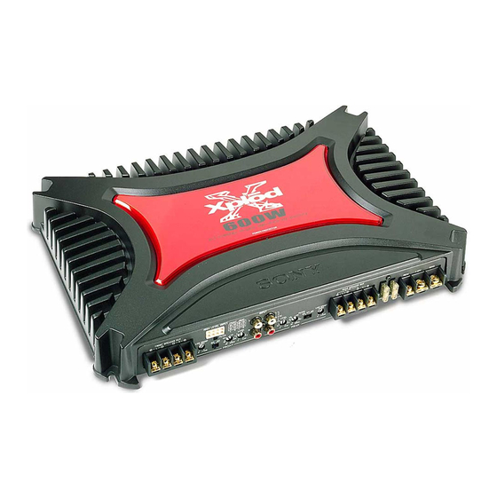
XM-4060GTX
SPECIFICATIONS
+0
dB)
–3
Input level adjustment range
0.3 – 6.0 V (RCA pin jacks)
1.2 – 12 V (High level input)
High-pass filter
50 – 300 Hz, –12 dB/oct
Low-pass filter
50 – 300 Hz, –12 dB/oct
Low boost
0 – 10 dB (40 Hz)
Power requirements
12 V DC car battery
(negative ground)
Power supply voltage
10.5 – 16 V
Current drain
at rated output : 31 A (4 Ω)
Remote input : 1 mA
Dimensions
Approx. 400 × 55 × 276 mm
(w/h/d) (15
3/4
projecting parts and controls
Mass
Approx. 4.6 kg (10 lb. 3 oz.) not incl. accessories
Supplied accessories
Mounting screws (4)
High level input cord (1)
Protection cap (1)
Design and specifications are subject to change without
notice.
STEREO POWER AMPLIFIER
US Model
Canadian Model
AEP Model
UK Model
E Model
× 2
× 10
in.) not incl.
1/4
7/8
1
Advertisement
Table of Contents

Related Manuals for Sony XM-4060GTX


Summary of Contents for Sony XM-4060GTX
- Page 1 Design and specifications are subject to change without Frequency response 5 Hz – 50 kHz ( notice. –3 Harmonic distortion 0.005% or less (at 1 kHz) STEREO POWER AMPLIFIER Sony Corporation 9-961-369-02 2005E04-1 e Vehicle Group © 2005. 05 Published by Sony Engineering Corporation...
-
Page 2: Table Of Contents
LES COMPOSANTS IDENTIFIÉS PAR UNE MARQUE 0 SUR LES DIAGRAMMES SCHÉMATIQUES ET LA LISTE DES PIÈCES SONT CRITIQUES POUR LA SÉCURITÉ DE FONCTIONNEMENT. NE REMPLACER CES COMPOSANTS QUE PAR DES PIÈCES SONY DONT LES NUMÉROS SONT DONNÉS DANS CE MANUEL OU DANS LES SUPPLÉMENTS PUBLIÉS PAR SONY. - Page 3 XM-4060GTX SECTION 1 GENERAL This section is extracted from instruction manual.
- Page 4 XM-4060GTX...
- Page 5 XM-4060GTX...
-
Page 6: Disassembly
XM-4060GTX SECTION 2 DISASSEMBLY Note : This set can be disassemble according to the following sequence. 2-1. BOTTOM PLATE (Page 6) 2-2. MAIN BOARD SECTION (Page 7) 2-4. LED BOARD 2-3. MAIN BOARD, (Page 8) HI-LEVEL BOARD (Page 7) Note : Follow the disassembly procedure in the numerical order given. - Page 7 XM-4060GTX 2-2. MAIN BOARD SECTION three screws screw 3 x 8) 3 x 8) three screws 3 x 8) 5 MAIN board section three screws 3 x 8) heat sink (main) 6 CN850 2-3. MAIN BOARD, HI-LEVEL BOARD 5 HI-LEVEL board...
-
Page 8: Led Board
XM-4060GTX 2-4. LED BOARD screw 2 LED board (+BT 3 x 6) light guide plate heat sink (main) -
Page 9: Electrical Adjustment
XM-4060GTX SECTION 3 ELECTRICAL ADJUSTMENT Bias Adjustment Note : The Bias adjustment should be performed only if any of Q109 and Q110 for RV104, Q209 and Q210 for RV204, Q309 and Q310 for RV304, and Q409 and Q410 for RV404 are replaced. -
Page 10: Diagrams
XM-4060GTX SECTION 4 DIAGRAMS • Semiconductor Location (MAIN SECTION) THIS NOTE IS COMMON FOR PRINTED WIRING BOARDS Ref. No. Location Ref. No. Location AND SCHEMATIC DIAGRAMS. (In addition to this, the necessary note is D101 D-10 Q201 H-12 D141 E-12... -
Page 11: Block Diagram
XM-4060GTX 4-2. BLOCK DIAGRAM (FRONT) S801-1 PRE AMP FILTER LINE AMP IC801 (1/2) IC806 (1/2) CN810 IC802 (1/2) LOW BOOST OVER LOAD CNJ100-1 LINE FRONT IC806 (2/2) SWITCH SPEAKER Q112 Q102 DIFFERENTIAL DRIVE POWER CNJ802 (1/2) RV801-2 FILTER Q103 Q107... -
Page 12: Printed Wiring Board -Main Section
XM-4060GTX 4-3. PRINTED WIRING BOARD — MAIN SECTION — • Refer to page 10 for Common Note on Printed Wiring Boards and Semiconductor Location. JW114 Q803 R806 JW115 Q813 R807 Q814 Q805 R829 R856 C807 C808 Q804 R809 Q812 Q850... -
Page 13: Schematic Diagram -Main Section (1/2)
XM-4060GTX 4-4. SCHEMATIC DIAGRAM — MAIN SECTION (1/2) — • Refer to page 10 for Common Note on Schematic Diagrams. R129 R133 C133 Q107 D101 R135 R151 R131 RV104 Q109 C125 R106 R137 R145 R117 Q112 Q102 C104 IC806(2/2) C123... -
Page 14: Schematic Diagram -Main Section (2/2)
XM-4060GTX 4-5. SCHEMATIC DIAGRAM — MAIN SECTION (2/2) — • Refer to page 10 for Common Note on Schematic Diagrams and IC Block Diagram. (Page 13) R856 R812 R821 CN851 CN850 C809 R827 C817 Q805 R800 R807 D811 R854 Q901... -
Page 15: Printed Wiring Boards -Hi-Level, Led Section
XM-4060GTX 4-6. PRINTED WIRING BOARDS — HIGH-LEVEL, LED SECTION — • Refer to page 10 for Common Note on Printed Wiring Boards. (Page 12) (Page 12) CNJ101 C220 JW313 JW314 R225 R325 R425 C218 C318 C217 C317 C118 C418 C117... -
Page 16: Exploded Views
XM-4060GTX SECTION 5 EXPLODED VIEWS NOTE: • The mechanical parts with no reference • Color Indication of Appearance Parts The components identified by mark 0 or dotted line with mark number in the exploded views are not supplied. Example : 0 are critical for safety. -
Page 17: Main Board Section
XM-4060GTX 5-2. MAIN BOARD SECTION not supplied (HI-LEVEL board) not supplied not supplied Ref. No. Part No. Description Remark Ref. No. Part No. Description Remark 3-262-164-01 PANEL, FRONT 3-225-183-31 SCREW (+PSW.TT.3XL) A-3274-684-A MAIN BOARD, COMPLETE 3-225-184-11 SCREW (+PS.TT.3XL) 3-249-924-01 BRACKET (HIGH LEVEL) -
Page 18: Electrical Parts List
XM-4060GTX SECTION 6 HI-LEVEL MAIN ELECTRICAL PARTS LIST NOTE: • Due to standardization, replacements in • Items marked “*” are not stocked since The components identified by mark 0 or dotted line with mark the parts list may be different from the they are seldom required for routine service. - Page 19 XM-4060GTX MAIN Ref. No. Part No. Description Remark Ref. No. Part No. Description Remark C215 1-163-251-11 CERAMIC CHIP 100PF C804 1-136-165-00 FILM 0.1uF C221 1-164-489-11 CERAMIC CHIP 0.22uF C806 1-115-339-11 CERAMIC CHIP 0.1uF C222 1-163-251-11 CERAMIC CHIP 100PF C807 1-162-962-11 CERAMIC CHIP...
- Page 20 XM-4060GTX MAIN Ref. No. Part No. Description Remark Ref. No. Part No. Description Remark < CONNECTOR > < PHOTO TRANSISTOR > CN850 1-506-468-11 PIN, CONNECTOR 3P IC902 8-719-800-42 PHOTO TRANSISTOR TLP521-1-A CNP101 1-784-917-11 PIN, CONNECTOR (PWB) 9P < JUMPER RESISTOR >...
- Page 21 XM-4060GTX MAIN Ref. No. Part No. Description Remark Ref. No. Part No. Description Remark Q310 8-729-053-85 FET IRF9540 R127 1-216-837-11 METAL CHIP 1/10W Q311 8-729-041-66 TRANSISTOR 2SC4015TV2 R128 1-216-829-11 METAL CHIP 4.7K 1/10W Q312 8-729-200-13 TRANSISTOR 2SC2712-Y R129 1-216-829-11 METAL CHIP 4.7K...
- Page 22 XM-4060GTX MAIN Ref. No. Part No. Description Remark Ref. No. Part No. Description Remark R301 1-216-837-11 METAL CHIP 1/10W R415 1-216-845-11 METAL CHIP 100K 1/10W R302 1-216-837-11 METAL CHIP 1/10W R416 1-216-845-11 METAL CHIP 100K 1/10W R303 1-216-845-11 METAL CHIP...
- Page 23 XM-4060GTX MAIN Ref. No. Part No. Description Remark Ref. No. Part No. Description Remark R847 1-216-827-11 METAL CHIP 3.3K 1/10W < TRANSFORMER > R850 1-216-833-11 METAL CHIP 1/10W R854 1-216-841-11 METAL CHIP 1/10W T801 1-439-636-11 TRANSFORMER, DC-DC CONVERTER R855 1-216-841-11 METAL CHIP...
- Page 24 XM-4060GTX MEMO...
- Page 25 XM-4060GTX US Model Canadian Model SERVICE MANUAL AEP Model UK Model E Model Ver. 1.1 2005. 05 SUPPLEMENT-1 File this supplement with the service manual. Subject : Change the MAIN, HI-LEVEL and LED boards. Printed wiring board and schematic diagram of new type, and changed parts list are described in this Supplement-1.
- Page 26 XM-4060GTX TABLE OF CONTENTS 1. Printed Wiring Board –Main Section– ........3 2. Schematic Diagram –Main Section (1/2)– ......4 3. Schematic Diagram –Main Section (2/2)– ......5 4. Printed Wiring Boards –High-Level, LED Section– ....6 5. Electrical Parts List ..............6 •...
- Page 27 XM-4060GTX 1. PRINTED WIRING BOARD — MAIN SECTION — • Refer to page 2 for Semiconductor Location. JW114 Q803 R806 JW115 Q813 R807 Q814 Q805 R829 R856 C807 R809 C808 Q804 Q812 Q850 JW92 R854 JW110 JW93 JW310 JW311 JW315...
- Page 28 XM-4060GTX 2. SCHEMATIC DIAGRAM — MAIN SECTION (1/2) — R129 R133 C133 Q107 D101 R135 R151 R131 RV104 C125 Q109 R106 R137 R145 R117 Q112 Q102 C104 IC806(2/2) C123 Q103 R140 R158 TP11 C102 IC802(1/2) R102 IC806(1/2) C106 C107 S801...
- Page 29 XM-4060GTX 3. SCHEMATIC DIAGRAM — MAIN SECTION (2/2) — • Refer to page 2 for IC Block Diagram. ((Page 4)) R856 R812 R821 CN851 CN850 C809 R827 C817 Q805 D811 R800 R807 R854 Q850 Q901 Q813 R818 R804 R855 C821...
- Page 30 XM-4060GTX HI-LEVEL MAIN 4. PRINTED WIRING BOARDS — HIGH-LEVEL, LED SECTION — 5. ELECTRICAL PARTS LIST NOTE: • Due to standardization, replacements in • Items marked “*” are not stocked since The components identified by mark 0 or dotted line with mark the parts list may be different from the they are seldom required for routine service.
- Page 31 XM-4060GTX MAIN Ref. No. Part No. Description Remark Ref. No. Part No. Description Remark C221 1-164-489-11 CERAMIC CHIP 0.22uF C806 1-115-339-11 CERAMIC CHIP 0.1uF C222 1-163-251-11 CERAMIC CHIP 100PF C807 1-162-962-11 CERAMIC CHIP 470PF C223 1-126-786-11 ELECT 47uF C808 1-162-962-11 CERAMIC CHIP...
- Page 32 XM-4060GTX MAIN Ref. No. Part No. Description Remark Ref. No. Part No. Description Remark CNP101 1-784-917-11 PIN, CONNECTOR (PWB) 9P < PHOTO TRANSISTOR > < JACK > IC902 8-719-800-42 PHOTO TRANSISTOR TLP521-1-A CNJ100 1-779-078-41 JACK, PIN 4P (INPUT) < JUMPER RESISTOR >...
- Page 33 XM-4060GTX MAIN Ref. No. Part No. Description Remark Ref. No. Part No. Description Remark Q310 8-729-053-85 FET IRF9540 R127 1-216-837-11 METAL CHIP 1/10W Q311 8-729-041-66 TRANSISTOR 2SC4015TV2 R128 1-216-829-11 METAL CHIP 4.7K 1/10W Q312 8-729-271-31 TRANSISTOR 2SC2713-G R129 1-216-829-11 METAL CHIP 4.7K...
- Page 34 XM-4060GTX MAIN Ref. No. Part No. Description Remark Ref. No. Part No. Description Remark R301 1-216-837-11 METAL CHIP 1/10W R415 1-216-845-11 METAL CHIP 100K 1/10W R302 1-216-837-11 METAL CHIP 1/10W R416 1-216-845-11 METAL CHIP 100K 1/10W R303 1-216-845-11 METAL CHIP...
- Page 35 XM-4060GTX MAIN Ref. No. Part No. Description Remark Ref. No. Part No. Description Remark R847 1-216-827-11 METAL CHIP 3.3K 1/10W < TRANSFORMER > R850 1-216-833-11 METAL CHIP 1/10W R854 1-216-841-11 METAL CHIP 1/10W T801 1-439-636-11 TRANSFORMER, DC-DC CONVERTER R855 1-216-841-11 METAL CHIP...
- Page 36 XM-4060GTX REVISION HISTORY Clicking the version allows you to jump to the revised page. Also, clicking the version at the upper on the revised page allows you to jump to the next revised page. Ver. Date Description of Revision 2003. 11 2005.
Need help?
Do you have a question about the XM-4060GTX and is the answer not in the manual?
Questions and answers