Philips LX7500R Service Manual
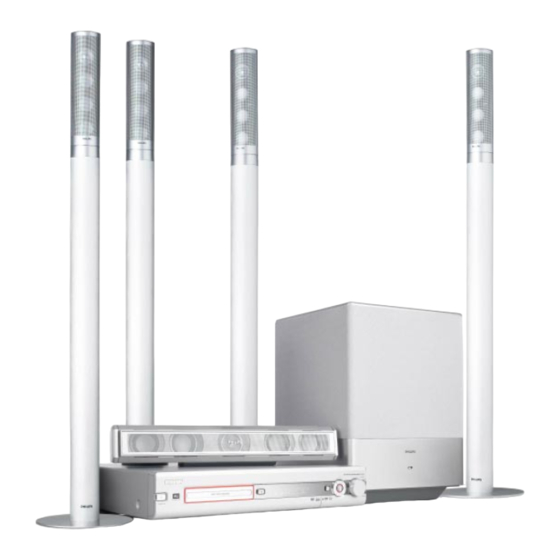
Dvd+rw receiver
Hide thumbs
Also See for LX7500R:
- Specifications (2 pages) ,
- User manual (70 pages) ,
- Quick use manual (7 pages)
Table of Contents
Advertisement
Quick Links
Download this manual
See also:
User Manual
DVD+RW Receiver
For servicing the DVD+RW Basic Engine we refer to
Service Manual 3122 785 14850
DVD+RW Basic Engine VAD8041
Only designated workshops can perform these repairs!
TABLE OF CONTENTS
Technical specification..........................................................2
Location of printed circuit boards..........................................4
Warnings & Safety ................................................................5
Brief Operating Instructions ..................................................6
Dismantling Instructions......................................................15
Service hints .......................................................................22
Diagnostic Software............................................................23
Block Diagrams...................................................................61
Wiring Diagram ...................................................................65
Exploded Views ..................................................................66
Circuit Diagrams and PWB Layouts
Switched Mode Power Supply ............................................69
Auxiliary Supply board ........................................................73
Display/Control board .........................................................75
Standby board ....................................................................76
Tray light boards left/right ...................................................76
©
Copyright 2004 Philips Consumer Electronics B.V. Eindhoven, The Netherlands
All rights reserved. No part of this publication may be reproduced, stored in a retrieval
system or transmitted, in any form or by any means, electronic, mechanical, photocopying,
or otherwise without the prior permission of Philips.
Published by MS 0448 Service Audio
Version 1.1
Printed in The Netherlands
Subject to modification
Combi board .......................................................................78
Amplifier board....................................................................87
Loudspeaker Socket board.................................................92
Analog Video (AV) board ....................................................93
µP Sub board (CECO) ......................................................101
Digital board......................................................................105
Alignments ........................................................................117
Circuit- and IC descriptions...............................................120
Abbreviations A/V-, Digital board......................................148
Spare parts list..................................................................150
Revision list.......................................................................181
LX7500R
/01/04/05
CLASS 1
LASER PRODUCT
©
3103 785 25301
Advertisement
Table of Contents

Related Manuals for Philips LX7500R


Summary of Contents for Philips LX7500R
-
Page 1: Table Of Contents
LASER PRODUCT © Copyright 2004 Philips Consumer Electronics B.V. Eindhoven, The Netherlands All rights reserved. No part of this publication may be reproduced, stored in a retrieval system or transmitted, in any form or by any means, electronic, mechanical, photocopying, or otherwise without the prior permission of Philips. -
Page 2: Technical Specification
Frequency response at SCART 1 (L+R) output :100 Hz - 12 kHz / 0± 3dB Pin Signals: S/N according to DIN 45405, 7, 1967 and PHILIPS standard test Audio R 1.8V RMS pattern video signal :FM: ≥ 50dB Audio R AM ≥... - Page 3 Technical specification LX7500R EN 3 Video - YC (Hosiden) Power Amplifier Input voltage Y :1Vpp ± 3dB Power stage protection : temperature and short circuit Input impedance Y :75 W Input voltage C :burst 300 mVpp ± 3 dB Output power (1kHz, 10% distortion)
-
Page 4: Location Of Printed Circuit Boards
EN 4 LX7500R Location of printed boards LOCATION OF PRINTED BOARDS top cover removed LS Sockets Audio Tuner AV Board below Combi Board Amplifier Board Combi Board Aux Supply DVD+RW Basic Engine AV3.5 Switched Mode Digital Board Power Supply figure 1... -
Page 5: Safety Information
Safety Information LX7500R EN 5 © ñ WARNING WAARSCHUWING All ICs and many other semiconductors are susceptible to Alle IC´s en vele andere halfgeleiders zijn gevoelig voor electrostatic discharges (ESD). Careless handling during electrostatische ontladingen (ESD). repair can reduce life drastically. -
Page 6: Brief Operating Instructions
The following excerpt of the Owner´s Manual serves as a very short introduction to the set. The complete Owners Manual can be downloaded in several languages from the Internet site of Philips Customer Care Center: www.p4c.philips.com Controls and connections 5 6 7 8 9... -
Page 7: Controls And Connections
Brief Operating Instructions LX7500R EN 7 Controls and connections 1 1 1 8 9 0 ! FOR PLAYBACK VIDEO OUT COMPONENT Connections on the rear MAINS ~ OUT / DIGITAL After all other connections have been made , connect to the digital coaxial input of digital equipment. -
Page 8: Remote Control
EN 8 LX7500R Brief Operating Instructions Remote control Remote control buttons REC/OTR starts recording the TV channel or the video source selected on the DVD recorder system. STANDBY 2 switches the DVD recorder system to standby . DVD/MON switches betw een the disc in the tray and the TV channel selected on the DVD recorder system. - Page 9 ™ SEARCH system. skips to the beginning of the next chapter/title/track, TV: enters the system menu of your Philips TV. searches forwards, 3, 4, 1, 2 tunes to a radio station with a higher frequency. move up,down ,left or right in a menu.
- Page 10 EN 10 LX7500R Brief Operating Instructions...
- Page 11 Brief Operating Instructions LX7500R EN 11...
- Page 12 EN 12 LX7500R Brief Operating Instructions Addendum LX7500R Attention – Atención – Achtung – Let op – Attenzione Viktigt – Vigtig – Huomio – Atenção 3103 605 2285.1 VieChr0441...
- Page 13 Brief Operating Instructions LX7500R EN 13...
- Page 14 EN 14 LX7500R Brief Operating Instructions...
-
Page 15: Dismantling Instructions
Dismantling Instructions LX7500R EN 15 DISMANTLING INSTRUCTIONS Dismantling the Top Cover Manual Opening the Tray • Remove 9 screws as shown in picture 1. In case the loader is defect or cannot be opened electrically, proceed • Release side walls on bottom and raise top cover as follows: upwards. - Page 16 EN 16 LX7500R Dismantling Instructions Dismantling the Digital Board Dismantling the DVD Basic Engine • Dismantle Top Cover as described before. • Dismantle the ornamental cover of the tray first (see picture 6). • Loosen 4 screws to dismantle Digital Board (see picture 7).
- Page 17 Dismantling Instructions LX7500R EN 17 Dismantling the DVD Basic Engine Dismantling the Amplifier Board (continued) • Remove 4 screws. • Turn the Amplifier Board out of the set and put it in service • Now the head of the last screw on the right side has become free position as shown in picture 14.
- Page 18 EN 18 LX7500R Dismantling Instructions Dismantling the Switched Mode Power Supply Board • Remove 4 screws as shown in picture 16 and loosen the ground wire from the cabinet. • Disengage catch of the airguide foils (see picture 17). • Lift the unit on the rear side and move it backwards to release the board from the catches on the front side (see picture 18).
- Page 19 Dismantling Instructions LX7500R EN 19 Dismantling the Front panel assembly • Dismantle the ornamental cover of the tray first (see picture 6). • Loosen 3 screws to bottom cabinet as shown in picture 20. • Release catches on both sides (see picture 21) and move the front panel out.
- Page 20 EN 20 LX7500R Dismantling Instructions Dismantling the Combi Board • Loosen 8 screws as shown in pictures 25 and 26. Note: The Combi Board is fixed with metal screws M3x4 and plastite screws 3x8. The metal screws are indicated with a text on the printed board and with a white ring on the rear plate →...
- Page 21 Dismantling Instructions LX7500R EN 21 Dismantling the Analog Video Board • Dismantle Combi Board and put it to rest (service) position as described before. The AV Board can now be accessed on the component side. To get access to the copper side: •...
-
Page 22: Service Hints
Due to this fact some rules have to be respected by the workshop during a repair: • Use only lead-free soldering-tin Philips SAC305 with order code 0622 149 00106. If lead-free solder-paste is required, please contact the manufacturer of your solder-equipment. -
Page 23: Diagnostic Software
The Demo mode can be switched on/off again via the System Menu of the set: Press System Menu on the remote control. Select A → w → Standby → Low power Normal Demo mode servtest LX7500R sh 1, 181004... - Page 24 Set_Fan_Ctrl which controls the speed of the set fan. In each test step of the temperature test the speed of the set fan can be set in four steps. servtest LX7500R sh 2, 041004...
- Page 25 See figure 2. fig. 2 PLAY button STOP button pressed? pressed? The DISPLAY test is intended to check the driver circuits and the LEDs for open- or short-circuits. Back to main menu. servtest LX7500R sh 3, 051004...
- Page 26 The correct tuner version is defined by the version detection resistor 3052 mounted on the Combi board. 3052 mounted = USA version without RDS. The stored preset frequencies serve as provision for other tuner modules only. servtest LX7500R sh 4, 091004...
- Page 27 1205 or 1701. In all test steps with digital input signal (2, 3, 4, 10 and 11) NO SIGNAL will be shown on the display when the SPDIF in/out IC 7603 does not recognize any signal. servtest LX7500R sh 5, 111004...
- Page 28 IIC bus. The functionality of these ICs can therefore not be tested with the IIC Test. For testing these ICs use the AUDIO TEST. STOP button pressed? Back to main menu. Back to main menu. servtest LX7500R sh 6, 111004...
- Page 29 Diagnostic Software LX7500R EN 29 5. Diagnostic Software Due to the complexity of the DVD recorder, the time to find a 5.1.2 Structure defect in the recorder can become long. To reduce this time, the recorder has been equipped with Diagnostic and Service software (DS).
- Page 30 EN 30 LX7500R Diagnostic Software Virgin mode 5.3.2 Error Handling Each nucleus returns an error code. This code contains six If you want that the recorder starts up in Virgin mode, follow this numerals, which means: procedure: • Unplug the recorder •...
- Page 31 Diagnostic Software LX7500R EN 31 Error messages startup Diversity String Input 1. Execute nucleus 1226 to enter the string. Please see adjustment instructions in chapter 8 for details Nucleus 1226 execution with string Figure 5-5 Error messages D&S program Figure 5-8 1.
- Page 32 EN 32 LX7500R Diagnostic Software Chrysalis (CHR) Nucleus Name DS_CHR_DevTypeGet Nucleus Number Description Sends the device ID and the module ids and revisions of the PNX7100 (Chrysalis) to the stdout port. User Input None Example DS:> 100 Device ID 7100 Codec ID PNX7100_MF2 F-BCU (0x0102) 1.0 INTC (0x011d) 1.0 PCI-XIO(0x0113) 1.0...
- Page 33 Diagnostic Software LX7500R EN 33 Example DS:> 102 010200: Test OK @ Nucleus Name DS_CHR_SineOn Nucleus Number Description Generate an audio sine signal on the audio output of the digital board. Note: Left channel 6kHz, right channel 12 kHz sine. Make sure to route the signal first.
- Page 34 EN 34 LX7500R Diagnostic Software Nucleus Name DS_CHR_MacroVisionOn Nucleus Number Description Turn on MacroVision. User Input None Example DS:> 110 011000: Test OK @ Nucleus Name DS_CHR_MacroVisionOff Nucleus Number Description Turn off MacroVision. User Input None Example DS:> 111 011100:...
- Page 35 Diagnostic Software LX7500R EN 35 Example DS:> 201 020100: Test OK @ NVRAM Nucleus Name DS_NVRAM_Communication Nucleus Number Description Check the communication between the IIC controller of the Chrysalis and the EEPROM User Input None Example DS:> 300 030000: Test OK @...
- Page 36 EN 36 LX7500R Diagnostic Software Description Check all data lines and address lines of the SDRAM User Input None Example DS:> 401 040100: Test OK @ Nucleus Name DS_SDRAM_Write Nucleus Number Description Write to a specific memory address User Input...
- Page 37 Diagnostic Software LX7500R EN 37 Nucleus Name DS_FLASH_CalculateChecksum Nucleus Number Description Calculate the checksum over all memory addresses. Used to check entire FLASH contents User Input None Example DS:> 504 050400: The Checksum = 0xBABE30A4 Test OK @ Nucleus Name...
- Page 38 EN 38 LX7500R Diagnostic Software Example DS:> 604 1 060400: Test OK @ Digital Video Input Output (DVIO) Nucleus Name DS_DVIO_LinkDevTypeGet Nucleus Number Description Get the device (revision) type information of the 1394 Link layer IC User Input None Example DS:>...
- Page 39 Diagnostic Software LX7500R EN 39 Progressive Scan (PSCAN) Nucleus Name DS_PSCAN_CommunicationDenc Nucleus Number Description Check the communication between the IIC controller of the chrysalis and the progressive scan DENC-IC User Input None Example DS:> 801 080100: Test OK @ Nucleus Name...
- Page 40 EN 40 LX7500R Diagnostic Software Nucleus Name DS_PSCAN_DevTypeGetDeinterlacer Nucleus Number Description Get the device (revision) type information of the progressive scan deinterlacer. User Input None Example DS:> 807 080700: Chip name : 2300 Chip version : 1 Test OK @...
- Page 41 Diagnostic Software LX7500R EN 41 User Input None Example DS:> 905 090500: Test OK @ Nucleus Name DS_BE_WriteReadDvdRw Nucleus Number Description Write data to and read data from a DVD+RW disc through the basic engine for verification of the writing...
- Page 42 EN 42 LX7500R Diagnostic Software Nucleus Name DS_BE_ErrorLogReset Nucleus Number Description Reset the error log in the basic engine User Input None Example DS:> 911 091100: Test OK @ Nucleus Name DS_BE_JitterOptimise Nucleus Number Description Perform jitter optimisation:A formatted DVD must be loaded into the engine before...
- Page 43 Diagnostic Software LX7500R EN 43 Nucleus Name DS_BE_RadialCalibration Nucleus Number Description Calibrate the radial loop User Input A formatted DVD must be loaded into the engine before executing this nucleus Example DS:> 919 091900: Test OK @ Nucleus Name DS_BE_Tilt...
- Page 44 EN 44 LX7500R Diagnostic Software Example DS:> 925 The entirely disc will be erased. Are you sure you want this?[y/n] 092500: Test OK @ Nucleus Name DS_BE_RegionCodeSet Nucleus Number Description Set the region code in the AV3. User Input Region code Example DS:>...
- Page 45 Diagnostic Software LX7500R EN 45 User Input None Example DS:> 1001100100: DCB version: 13Test OK @ Nucleus Name DS_DCB_LightDisplay Nucleus Number 1002 Description Light the entire display of the DCB, and clear the display after confirmation.User confirmation is necessary. User Input...
- Page 46 EN 46 LX7500R Diagnostic Software Example DS:> 1102 110200: Test OK @ Nucleus Name DS_ANAB_CommunicationIicDataSlicer Nucleus Number 1103 Description Check the communication between the digital board and the data slicer on the analogue board User Input None Example DS:> 1103...
- Page 47 Diagnostic Software LX7500R EN 47 Nucleus Name DS_ANAB_SoftwareVersionDiagnosticsGet Nucleus Number 1110 Description Get the software version of the diagnostic software of the analogue board User Input None Example DS:> 1110 111000: Diagnostics application version : 11.00.13 Test OK @ Nucleus Name...
- Page 48 EN 48 LX7500R Diagnostic Software Input signal is from REAR VIDEO(CVBS) IN and will be routed to the digital board. Input signal is from FRONT S-VIDEO(Y/C) IN and the signal received will be routed to the digital board. Input signal is from REAR S-VIDEO(Y/C) IN and will be routed to the digital board.
- Page 49 Diagnostic Software LX7500R EN 49 Input Audio Signal is routed from FRONT Cinch In to Digital Board.(This is same as path ID Input Signal is from Rear Cinch In1 and it will be routed to Digital Board.. No routing. No routing.
- Page 50 EN 50 LX7500R Diagnostic Software Nucleus Name DS_ANAB_ClockReference Nucleus Number 1117 Description Generate a 1 kHz signal on pin 7 (INT) of the clock IC User Input None Example DS:> 1117 111700: Test OK @ Nucleus Name DS_ANAB_ClockCorrection Nucleus Number...
- Page 51 Diagnostic Software LX7500R EN 51 Byte containing 8 bit fields for TRUE/FALSE : BIT 0: Decoder BIT 1: Modulation BIT 2: NICAM NICAM/stereo bit for Europe SAP/stereo bit for NAFTA BIT 3: Satpreset BIT 4: Presetdefined Preset defined bit is only used for Europe. For NAFTA,...
- Page 52 EN 52 LX7500R Diagnostic Software Example DS:> 1204 120400: Software Diagnostics Version = 0001 Test OK @ Nucleus Name DS_SYS_EepromUpload Nucleus Number 1205 Description Upload the contents of the NVRAM on the analogue board or the digital board to the...
- Page 53 Diagnostic Software LX7500R EN 53 Example DS:> 1210 0 0xa0 1 121000: Value read =0x06T est OK @ Nucleus Name DS_SYS_UartWrite Nucleus Number 1211 Description Perform an UART write action on the digital board on a specified UART User Input The user inputs the UART to write to, the number of bytes and the bytes to be written to the UART.
- Page 54 EN 54 LX7500R Diagnostic Software Example DS:> 1215 cvbs ntsc 121500: Test OK @ DS:> 1215 cvbs pal 121508: The VideoInputProcessor cannot detect a sync-signal. Error @ DS:> 1215 yuv ntsc 121511: Error in luminance signal(Y) Error in chrominance signal(U)
- Page 55 Diagnostic Software LX7500R EN 55 Nucleus Name DS_SYS_DisplayFatalOn Nucleus Number 1223 Description Turn on the display-fatal functionality which displays debug-information on the display when encountering a fatal error condition from which could not be recovered automatically User Input None Example DS:>...
- Page 56 EN 56 LX7500R Diagnostic Software Example DS:> 1229 122900: 6D7920626F61726400020300010101020101000020080000 Test OK @ Nucleus Name DS_SYS_AudioLoopThroughStart Nucleus Number 1230 Description Description: The audio input is routed from the an input to all outputs. Input is set with the routing nucleus 1113. All outputs are enabled.
- Page 57 Diagnostic Software LX7500R EN 57 Nucleus Name DS_SYS_SettingsDoubleCheck Nucleus Number 1233 Description This nucleus sets the HW-Id in the HW-diversity string User Input <HW-ID> - The hardware ID to set -No input - The user will be asked for the ID Example DS:>...
- Page 58 EN 58 LX7500R Diagnostic Software Example DS:> script Executing User/Dealer script. Busy executing NUC1100 1-28 Hello Analogue Board Busy executing NUC1000 2-28 Busy executing NUC200 3-28 Busy executing NUC1228 4-28 Settings ID: 4C4541440D00000000030300010101020101000020080000 Board name: LEAD Hardware ID: 0 Codec IC: PNX7100_MF3...
- Page 59 Diagnostic Software LX7500R EN 59 Example Busy executing NUC601 16-28 Busy executing NUC700 17-28 Device type of the link layer IC: ffc00301 Busy executing NUC701 18-28 Device type of the phy layer IC: 0 Busy executing NUC702 19-28 Busy executing NUC703 20-28...
- Page 60 EN 60 LX7500R Diagnostic Software...
-
Page 61: Block Diagrams
CLOCK & BACKUP STBY CONTROL µP to sheet 2, 1300 AUX. Supply board 1986 5N_STBY COMPONENT VIDEO OUT 5V_STBY Block diagram 1 LX7500R, 251104 33V_STBY VIDEO AUDIO I2S 1946 1947 1900 to sheet 2, 1900 Dig. board to sheet 2, 1104Dig. board to sheet 2, 1904 Dig. - Page 62 1904 Dig. board separate block diagram to 1704 Dig. board 1102 1600 from sheet 1, 1900 A/V board Block diagram 2 LX7500R, 221104 from sheet 1, 1986 uP sub- board from sheet 1, 1947 A/V board from sheet 1, 1946 A/V board...
- Page 63 AD_ACLK A_YCVBS F4709 D_CVBS F4712 D_C F4716 D_R F4718 D_B F4722 DVD PART LX7500R, 09112004 A: DC, 200mV/Div 2V / div AC 50ns / div A: DC, 200mV/Div A: DC, 200mV/Div 2V / div AC 10us / div 2V / div AC 200ns / div...
-
Page 64: Digital Board
Audio (M24C16) Supply VSA1 (STV6618) (HEF IC'S) (for EUROPE VSA2 only) ASC1S For EUROPE only AKILL Combi Board EEPROM Combi µP (M24C02) TMP88CU74F IPOR_DC POR_DC Display Control Board Front µP Display TMP87CH74F Blockdiagram Control lines and bus systems LX7500R, 09112004... -
Page 65: Wiring Diagram
PH SIDE ENTRY XH SIDE ENTRY FLASH TOP ENTRY FFC TOP ENTRY 1.0 FFC SIDE ENTRY 1.0 SPECIAL HEADER FFC 1 to 1 (AD) FFC 1 to n (BD) 8001 3103 308 9419. 8041 3103 308 9488. wiring diagram LX7500R, 181104... - Page 66 3103 604 00622 FOOT, RUBBER Pl.3x8 201-3 3103 607 50491 FOOT ASSY 201-2 3103 607 90941 ORNAMENTAL COVER, TRAY LX7500R 215 ! 2422 070 98231 MAIN SCORD, IEC M3x4 215 ! 2422 070 98236 MAINS CORD, UK 3103 607 10051 FAN 60X60X20...
- Page 67 Pl. 3x8 3103 607 51321 KNOB VOLUME 8020 3103 308 94411 FIREWIRE CABLE, 650mm, EEE1394 Only those parts of which a service code number is stated are normal service parts. Pl. 3x8 8020 Pl. 2,5x8 EV2 front complete LX7500R, 270904...
- Page 68 3103 607 51391 DOOR FRONT, LX7500/01/04 3103 607 51421 DOOR FRONT, LX7500/05 3103 604 00441 HINGE, DOOR FRONT Only those parts of which a service code number is stated are normal service parts. Pl. 2x6 EV3 front assy mech. LX7500R, 280904...
- Page 69 Switched Mode Power Supply FOR ORIENTATION ONLY SMPS "AC6191" Drawing 1 +27,6V 307V -27,6V 4,8V -5,2V 5,2V 12,3V 12,3V 33,6V -27,7 3,7V TL494CN (MOTOROLA) Pulse with modulator VOLTAGE SENSE ...V DC voltages measured in Stop mode with no audio output. SMPS LX7500R, 221104 (original status 080904)
-
Page 70: Circuit Diagrams And Pwb Layouts Switched Mode Power Supply
Circuit Diagrams and PWB Layouts LX7500R EN 70 Switched Mode Power Supply FOR ORIENTATION ONLY SMPS "AC6191" Drawing 2 230V 120V 120/230V SMPS AC6191 (LX7500R), 221104 original status 080904... - Page 71 Circuit Diagrams and PWB Layouts LX7500R EN 71 Switched Mode Power Supply FOR ORIENTATION ONLY SWITCHED MODE POWER SUPPLY / component side view SMPS AC6191 (LX7500R), 150904 original status 080904...
- Page 72 Circuit Diagrams and PWB Layouts LX7500R EN 72 Switched Mode Power Supply FOR ORIENTATION ONLY SWITCHED MODE POWER SUPPLY / copper side view SMPS AC6191 (LX7500R), 150904 original status 080904...
- Page 73 3339 A5 2312 3340 B5 10u 16V 3341 C5 0,1V BZX384-C6V8 3322 3342 C7 +12V_A ...V DC voltages measured in Stop mode # for provision only with no audio output. 4000 A8 6301 4001 A8 AUX SUPPLY BOARD LX7500R, 241104...
- Page 74 Circuit Diagrams and PWB Layouts LX7500R EN 74 1300 A1 6305 A2 1301 A2 7301 A2 1303 A1 7303 A1 AUX. SUPPLY BOARD / component side view 1304 A2 7304 A1 1305 A3 7306 A1 1306 A2 7308 A3 1307 A3...
-
Page 75: Display/Control Board
VOLUME P4<0:7> P9<0:7> 6105 B14 6106 C14 6109 G8 EC12 6110 D7 0303 6111 E4 BARCODE 6112 E3 P5<0:3> 7100 A5 GND GND 7101 B13 7102 D13 7103 E11 7104 F4 7105 E3 Display board .6 LX7500R, 221104 7106 E7... -
Page 76: Standby Board
HP_RIGHT GND_FC 5203 F2212 F2215 06FE-BT-VK-N TC38-103-01 Display board .6 LX7500R, 230904 tray light left board LX7500R .6, 240904 tray light right board LX7500R .6, 240904 1130 C1 1931 A4 3301 A3 3303 B3 7300 A3 F3001 A1 F3003 B1... - Page 77 DISPLAY/CONTROL BOARD / copper side view to AV board to COMBI board to STBY board to COMBI board Front Display board LX7500R .6, 240904 DISPLAY/CONTROL BOARD / component side view to STBY board to COMBI board PLAY to COMBI board...
-
Page 78: Combi Board
2,5V 2,3V 3082 G11 F195 H7 3117 2042 3083 G11 F196 H7 /37 only 3084 G3 F197 H7 3085 G7 F198 I7 Combi board LX7500R, 181004 3086 G7 F199 H7 3087 G7 3088 G6 3089 G7... - Page 79 3224 C12 DAC_SL 470R 3225 C2 2353 # for provision only ...V DC voltages measured in Stop mode with no audio output. 3226 C14 3227 C10 3228 C11 /37 only 3229 C9 GND_ALR GND_AS Combi board LX7500R, 181004 3230 C2...
- Page 80 3448 F6 F325 06FE-ST-VK-N 3449 H10 4304 3450 I9 GND_ALR GND_HP 3451 H11 3452 F11 ...V DC voltages measured in Stop mode # for provision only 4305 3453 G10 with no audio output. 3454 H10 Combi board LX7500R, 181004 3455 H11...
- Page 81 100p 3615 1,5V 3616 1,5V LM833D 1,5V GND_ALR 7414-1 1,5V 7414-2 3617 LM833D GND_ALR +OP_DAC ADC_IN_L 2455 +OP_DAC # for provision only ...V DC voltages measured in Stop mode with no audio output. 100p GND_ALR Combi board LX7500R, 221104 GND_ALR...
- Page 82 SPDIF_ERF_3V3 F547 SDO1 F521 100R 3766 100R 3722 3854 F544 SDO0 F522 GPIO SDI<0:3> SCAN SCAN ESAI_1 3768 PLL_GND IO_GND CORE_GND # for provision only ...V DC voltages measured in Stop mode with no audio output. Combi board LX7500R, 221104...
- Page 83 3826 C5 3118 7609-5 3827 C7 74LVU04D 100R 3828 C6 3829 C9 ...V DC voltages measured in Stop mode DIG DIG with no audio output. 3830 C1 3832 C4 3833 C6 3834 C4 # for provision only Combi board LX7500R, 221104...
- Page 84 F718 E2 F719 E2 F720 E2 F721 E2 F722 F2 ...V DC voltages measured in Stop mode # for provision only F723 F12 with no audio output. F724 G12 F725 G2 Combi board LX7500R, 081004 F726 H2 F727 G12 F728 D10...
- Page 85 SOURCE SEL. SOUND PROC. IC SUBWOOFER/ CENTER µP 1100 1020 1205 1810 1302 Combi board LX7500R .4 , 071004 This assembly drawing shows a summary of all possible versions. For components used in a specific version see schematic diagram respectively partslist.
- Page 86 Aux supply board to Front board 1950 & 1953 1305 1304 1910 Combi board LX7500R .4 , 081004 This assembly drawing shows a summary of all possible versions. For components used in a specific version see schematic diagram respectively partslist.
- Page 87 Circuit Diagrams and PWB Layouts LX7500R EN 87 6-channel class-D amplifier Basic operation of a class-D amplifier Basically, the output stage of a class-D amplifier outputs a continuous square wave swinging between positive and negative power supplies with a fixed frequency (“clock” frequency) far beyond the audible range. The duty cycle of this square wave is modulated with the audio signal.
- Page 88 Circuit Diagrams and PWB Layouts LX7500R EN 88 MECHANICAL EXPLODED VIEW Block diagram and operation SINGLE ENDED 6 x 75W/100W BRIDGE 3 x 100W TDA8920/TDA8924 TDA8920 output 1 output 1 input 1 input 1 output 2 input 2 TDA8920/TDA8924 TDA8920...
-
Page 89: Amplifier Board
DC voltages measured in Stop mode 3106 D6 F135 L12 3107 B8 F139 B12 with no audio output. 3108 B6 F140 C2 3109 E8 F141 F3 6x100W amplifier LX7500R, 210904 Vss Vss 3151 C11 F142 F2 3152 D11 F143 K3 3153 C11... - Page 90 Circuit Diagrams and PWB Layouts LX7500R EN 90 AMPLIFIER BOARD / component side view This assembly drawing shows a summary of all possible versions. 3139 113 3526 pt3 dd wk0345 For components used in a specific version see schematic diagram and respective parts list.
- Page 91 Circuit Diagrams and PWB Layouts LX7500R EN 91 AMPLIFIER BOARD / copper side view This assembly drawing shows a summary of all possible versions. For components used in a specific version see schematic diagram and respective parts list. 3139 113 3526 pt3 dd wk0345...
- Page 92 WH08D-1 LS SOCKET BOARD / component side view LS SOCKET BOARD / copper side view Center LQR3215-0402F 1936 2932 GND SL 2933 GND SR 1931 WH08D-1 LQR3215-0102F satellite, center and sub-woofer LS socket board LX7500R, 210904 Grey Blue Green Purple...
- Page 93 1703 G3956M K3953M G3956M ..V MEASURED IN RECORD MODE L’ 1704 TPS 5,5 MHz TPS 5,5 MHz 1706 TPS 6,0 MHz 3731 270R 330R 270R 4700 4701 7709 TDA9818 SFS_TS for MSTD only 7710 TDA9817 TDA9817 A/V board LX7500R, 231104...
- Page 94 F4207 F1 from/to uP Board from/to uP Board from/to uP Board to Digital Board from/to uP Board from / to Digital Board F4209 F1 A/V board LX7500R, 231104 F4210 E1 F4505 I3 F4707 I9 I465 I461 I462 I463 A_CVBS I405...
- Page 95 7508 D9 A: DC, 500mV/Div 7509 F2 500us/Div 7511 F4 F501 E2 OSCILLOGRAMS 5NSTBY F502 E2 ..V MEASURED IN PLAYBACK MODE F504 D2 ..V MEASURED IN RECORD MODE I501 C2 I502 D2 A/V board LX7500R, 231104 I503 D2 I504 D2...
- Page 96 1600 I631 E2 I610 I611 18M432 ...V DC voltages measured in Stop mode with no audio output. 5601 I612 5602 I613 A/V board LX7500R, 241104 OSCILLOGRAMS ..V MEASURED IN PLAYBACK MODE ..V MEASURED IN RECORD MODE A/V board LX7500R, 241104...
- Page 97 3932 SDASW 100R I998 I992 3933 RESERVED I994 2936 TEST I991 CBLK I956 2942 2944 I958 VSSA VSSD VSSO 2937 I995 I957 3940 2945 3941 I959 2943 L1101-95264-0E1 180p 180p A/V board LX7500R, 221104 3946 3947 A/V board LX7500R, 231104...
- Page 98 3026 F7 I013 3027 C7 7005 100n UDA1361TS 3029 D8 Φ 3030 D8 VDDD VDDA 3034 F8 24-BIT AUDIO 3035 F9 A/V board LX7500R, 231104 3039 F8 SYSCLK I028 I030 I014 3041 4004 2029 3041 E8 DATAO VINR ARADC 3043 D2...
- Page 99 FRONT/DISPLAY BOARD 1922 DIGITAL BOARD 1900 AUX SUPPLY BOARD 1300 This assembly drawing shows a summary of all possible versions. A/V board LX7500R .4, 231104 For components used in a specific version see schematic diagram respectively partslist. TEST POINTS F 011...
- Page 100 F4722 F4720 I502 I723 This assembly drawing shows a summary of all possible versions. A/V board LX7500R .4, 231104 For components used in a specific version see schematic diagram respectively partslist. TEST POINTS F 010 A7 F 501 A5 F4714 B3...
- Page 101 100R 7819 I818 A_YCVBS BC857BW from B2 100R GNDD GNDD GNDD GNDD GNDD from / to IOV from / to IOV from / to IOV GNDD GNDD GNDD GNDD GNDD A: DC, 1 V/Div 20us/Div µP Sub board LX7500R, 231104...
- Page 102 I905 for SET FAN only 6903 from CECO BAV70W 3927 GNDD 12VSTBY 12VSTBY 7902-4 LM324D GNDD GNDD 7902-2 LM324D F910 GNDD I906 6901 BAV70W GNDD GNDD 3921 I907 GNDD BE_FAN 470R to CECO not used µP Sub board LX7500R, 231104...
- Page 103 Circuit Diagrams and PWB Layouts LX7500R EN 103 uP Sub Board: (top view) uP Sub Board: (bottom view)
- Page 104 Circuit Diagrams and PWB Layouts LX7500R EN 104 uP Sub Board TESTPOINT OVERVIEW F8001 C3 F831 C1 F8610 C3 I808 A3 F8002 C3 F832 A2 F8701 A1 I809 C1 F8003 C3 F833 C1 F8702 A3 I810 B3 F8004 C3 F834 A1...
-
Page 105: Digital Board
Circuit Diagrams and PWB Layouts LX7500R EN 105 DIGITAL BOARD Chrysalis PPS E4 AV3+ 1100 A10 4117 E6 1102 B14 4118 F8 1103 H14 4119 F8 1104 G9 4121 H6 VDD_PNX_PAD 1105 B10 4122 B5 2108 7103 1106 I5 4123 B5... - Page 106 Circuit Diagrams and PWB Layouts LX7500R EN 106 DIGITAL BOARD Chrysalis PPS E4 AV3+ 1201 D1 3289 H13 1203 A1 3290 I13 2200 B2 3291 I13 2201 C2 3292 I13 2202 D1 3293 I13 +3V3_IEEE_A +3V3_IEEE_D +3V3_IEEE_PLL +3V3_IEEE_D +3V3_IEEE_D +3V3_IEEE_D...
- Page 107 Circuit Diagrams and PWB Layouts LX7500R EN 107 DIGITAL BOARD Chrysalis PPS E4 AV3+ 2300 A3 2301 A4 2302 B2 2303 C1 4304 2304 B4 PLL_OUT 2305 C1 not used 2306 C2 FSCLK3_OUT 2307 E3 I300 5300 2308 F7 4314...
- Page 108 Circuit Diagrams and PWB Layouts LX7500R EN 108 DIGITAL BOARD Chrysalis PPS E4 AV3+ 1400 C14 3490 E11 1401 I5 3491 E10 2400 A9 3492 E11 PCI_AD(31:0) VDD_PNX_PAD 2401 A9 3493 E10 PCI_CON SDRAM 2402 A9 3494 E11 I418 3400...
- Page 109 F1509 2521 I506 B5 I507 B6 100n I508 C2 I509 C2 not used 2524 I510 C3 4500 I511 D2 B12B-PH-SM3-TBT 100n I512 D3 I511 I512 1507 1000mA 1501 1502 1503 1504 2525 100n F1512 2526 100n Digital board LX7500R, 241104...
- Page 110 Circuit Diagrams and PWB Layouts LX7500R EN 110 DIGITAL BOARD Chrysalis PPS E4 AV3+ 1704 D13 I727 C9 2700 B4 I728 E8 2701 G11 I729 E9 I730 C2 2703 D5 2704 B4 I731 C2 2705 C5 I732 C2 2706 B2...
- Page 111 Circuit Diagrams and PWB Layouts LX7500R EN 111 DIGITAL BOARD Chrysalis PPS E4 AV3+ 0605 E3 0609 F3 2806 A12 2807 A13 2808 A12 +3V3 VDD_NOR 2809 A13 5803 I805 2810 A12 7807 VDD_NOR 2811 A13 7805 PCI_AD(31:0) PCI_AD(31:0) PCI_AD(31:0)
- Page 112 Circuit Diagrams and PWB Layouts LX7500R EN 112 DIGITAL BOARD Chrysalis PPS E4 AV3+ 1900 E14 5913 H4 1901 G13 5914 F10 1904 A14 5915 F10 2036 I5 5916 H13 2046 G12 7900 E9 2900 A4 7901 F9 2901 A4...
- Page 113 Circuit Diagrams and PWB Layouts LX7500R EN 113 DIGITAL BOARD Chrysalis PPS E4 AV3+ 1000 B2 F011 D13 1001 G9 F012 F9 2000 B3 F013 H3 F014 H3 2001 B3 I002 2002 B3 F015 H3 3023 VDDA_7118 2003 B4 F016 H3...
- Page 114 3216 A1 3445 D1 3908 A3 5906 A1 2731 A3 3217 B1 3446 D1 3909 A1 5908 A3 Digi board Chrysalis LX7500R, 191004 2832 D2 3218 B1 3447 D2 3910 A1 5909 A1 2833 D2 3220 B1 3448 D2 3911 A3...
- Page 115 4906 A1 2416 C2 3093 B1 3717 A2 4910 A2 2417 C2 3095 B3 3718 A2 4911 A3 Digi board Chrysalis LX7500R, 191004 2418 C3 3096 C3 3721 A2 4912 A2 2419 C3 3097 B1 3722 A2 5001 A1 2420 C2...
- Page 116 Circuit Diagrams and PWB Layouts LX7500R EN 116 DIGITAL BOARD / TESTPOINT OVERVIEW I227 B3 I504 C1 I745 A5 F0001 C1 F0238 D1 F1510 B1 I009 A1 F0003 C1 I300 B3 I505 C1 I746 A2 F0239 D1 F1512 A1 I010 A1...
-
Page 117: Alignments
Alignments LX7500R EN 117 8. Alignments Alignment Instructions Analog Board Test equipment: 2 HF - AGC adjustment [3724]: 1. Dual-trace oscilloscope Service tasks after replacement of IC 7710: Voltage range : 0.001 ~ 50 V/div Frequency : DC ~ 50 MHz Purpose: Set amplifier control. - Page 118 The slash version is stored with command 1217, followed by the slash version as parameter. The NVM, item 7808, on the Microprocessor Sub board The slash versions used in LX7500R are the following: contains the following factory settings: • LX7500R/01: 35 1.
- Page 119 Alignments LX7500R EN 119 – 05 = change code (this is not used for this calculation) – 01 = YEAR – 36 = Production WEEK – 130156 = Lot and SERIAL number 2. Calculate the unique number: this number always exists out of 10 hexadecimal numbers.
- Page 120 EN 120 LX7500R Circuit-, IC descriptions and list of abbreviations 9. Circuit-, IC descriptions and list of abbreviations Display Board 9.1.7 REC-LED The REC-LED-ring is made with 3 red LED, controlled via pin 9.1.1 Microcontroller 3 (only for flashing) and pin 12 for on/off switching, of the microcontroller.
- Page 121 Circuit-, IC descriptions and list of abbreviations LX7500R EN 121 [1986]). By generating a high level on pin 16 of the CC the A quasi-split audio system is used. Separate surface-wave digital PCB can be reset (inverter [7817] in between).
- Page 122 EN 122 LX7500R Circuit-, IC descriptions and list of abbreviations 9.3.3 Audio routing TR 01055_001 170502...
- Page 123 Circuit-, IC descriptions and list of abbreviations LX7500R EN 123 The processing of audio is always done in stereo (e.g. separate “DIGITAL IN”). The capacitors [2256] and [2266] perform an left- and right-channel) and the complete switching is realized AC-coupling between connector- and set-ground. The second by using HEF4052, which is a dual four-to-one multiplexer.
- Page 124 EN 124 LX7500R Circuit-, IC descriptions and list of abbreviations (“D_IKLL”-line) or the “IPFAIL”-signal from power-supply-unit (in this case it’s the combination of “A_KILL” and “IPFAIL”). In addition to that the DAC [7001] and the cinch outputs can be killed (muted) in case of “digital silence” by the circuit around [7008], [7009] and [7010], when no audio data are available (e.g.
- Page 125 Circuit-, IC descriptions and list of abbreviations LX7500R EN 125 9.3.5 Video-routing Figure 9-1...
- Page 126 EN 126 LX7500R Circuit-, IC descriptions and list of abbreviations The Video-I/O-switching is basically realized by the matrix 9.3.7 Analog Follow-Me switch STV6618 [7408], which is controlled via I C-bus by the CC. All used outputs excluding pin 21 (Y/CVBS-REC) have a 6 This circuit compares the video signal from the internal dB-amplification and a 75 Ohms driver-stage inside.
- Page 127 Circuit-, IC descriptions and list of abbreviations LX7500R EN 127 9.4.2 Audio routing TR 01057_001 170502 Figure 9-2...
- Page 128 EN 128 LX7500R Circuit-, IC descriptions and list of abbreviations The sound processing is always done in stereo (that means in parallel. To avoid plops and any other audible noise on the separate left- and right-channel). output there is a mute-stage implemented [7509], [7511] for each channel.
- Page 129 Circuit-, IC descriptions and list of abbreviations LX7500R EN 129 9.4.4 Video-routing Figure 9-3...
- Page 130 EN 130 LX7500R Circuit-, IC descriptions and list of abbreviations Digital Board Chrysalis F The Video-I/O-switching is basically realized by the matrix switch STV6618 [7408], which is controlled via I C-bus by the 9.5.1 Introduction CC. All used outputs excluding pin 21 (Y/CVBS-REC) have a 6dB-amplification and a 75 Ohms-driver-stage inside.
- Page 131 Circuit-, IC descriptions and list of abbreviations LX7500R EN 131 9.5.2 Record Mode Block diagram Chrysalis Digital Board TO/FROM BE AV3 OPTIONAL HDD, PCMCIA BE AV2 IDE CONNECTOR UART I2S EEPROM EEPROM 64Kbit 64Kbit I2C 0 I2C 0 I2C0 7004...
- Page 132 EN 132 LX7500R Circuit-, IC descriptions and list of abbreviations 9.5.4 Clock Distribution Clock distribution on Chrysalis board 24.576 MHz BE INTERFACE 7004 VIP7118 7400 7703 7804 133MHz SDRAM ADV7196 CHRYSALIS 7812 PNX7100 SDRAM 7201 1394 LINK 7200 1394 PHY...
- Page 133 Circuit-, IC descriptions and list of abbreviations LX7500R EN 133 9.5.7 Reset Reset concept Chrysalis board Reset_IDEn 7104-3 & Reset_1394n 7400 7104-4 & 7106 NCP303 >1 PNX7100_Resetn Reset_BEn 7107-1 & Reset_PSn 7107-2 CHRYSALIS GPIO & PNX7100 Analog_Resetn 7107-3 & VIP_Resetn 7104-1 &...
- Page 134 EN 134 LX7500R Circuit-, IC descriptions and list of abbreviations Service UART Interface Logic IC 74HCT14D (item 7111) is used to make a level conversion from microprocessor (LVTTL) to +/-5V (compatible with most RS232 interfaces) and vice versa. The control line MPIO19_CTL_SERVICE is used to activate service and diagnostic SW at start up procedure.
- Page 135 Circuit-, IC descriptions and list of abbreviations LX7500R EN 135 IC Descriptions 9.8.1 Display Board IC 7103 TMP87CH74F Display Board, Front Microprocessor Figure 9-8...
- Page 136 EN 136 LX7500R Circuit-, IC descriptions and list of abbreviations Figure 9-9...
- Page 137 Circuit-, IC descriptions and list of abbreviations LX7500R EN 137 Figure 9-10...
-
Page 138: Pin Description
EN 138 LX7500R Circuit-, IC descriptions and list of abbreviations 9.8.2 IC’s Analog Board IC7408: STV6618 Analog Board, Video Switch Matrix Pin Description Pin No. Symbol Description Y/CVBSIN_TUN Y/CVBS Input from Tuner DIGOUT3 Digital Output Pin 3 GND1 Ground Supply 1 for Video Inputs... - Page 139 Circuit-, IC descriptions and list of abbreviations LX7500R EN 139 Pin No. Symbol Description +5 V Digital Power Supply I²C Bus Clock I²C Bus Data GNDD Digital Ground Supply CIN_TV Chroma Input from TV (SCART1 or external Cinch) Y/CVBSIN_TV Y/CVBS Input from TV (SCART1 or external Cinch)
- Page 140 EN 140 LX7500R Circuit-, IC descriptions and list of abbreviations Figure 3: STV6618 Block Diagram DIGOUT6 DIGOUT5 DIGOUT4 DIGOUT3 DIGOUT2 DIGOUT1 C_GATE...
- Page 141 Circuit-, IC descriptions and list of abbreviations LX7500R EN 141 IC7411: NJM2285 Analog Board, Video Switch...
- Page 142 EN 142 LX7500R Circuit-, IC descriptions and list of abbreviations IC7313 TEA 1507 Analog Board, Power Supply Control BLOCK DIAGRAM andbook, full pagewidth...
- Page 143 Circuit-, IC descriptions and list of abbreviations LX7500R EN 143 IC7404: AD1582 Analog Board, Digital/Analogue Converter FUNCTIONAL BLOCK DIAGRAM CLOCK DIGITAL CONTROL DATA SUPPLY INPUT VOLUME MUTE SERIAL CONTROL VOLTAGE AUTO-CLOCK AD1852 REFERENCE DIVIDE CIRCUIT INTERFACE 16-/18-/20-/24-BIT MULTIBIT SIGMA- ATTEN/...
- Page 144 EN 144 LX7500R Circuit-, IC descriptions and list of abbreviations AD1852 PIN FUNCTION DESCRIPTIONS Input/Output Pin Name Description DGND Digital Ground. MCLK Master Clock Input. Connect to an external clock source at either 256 F , 384 F 512 F...
- Page 145 Circuit-, IC descriptions and list of abbreviations LX7500R EN 145 9.8.3 ICs Digital Board Chrysalis IC7106 NCP303LSN29, Digital Board 2.1 Chrysalis, Reset Circuit NCP303LSNxxT1 Open Drain Output Configuration Input Reset Output IC7501 NCP1570D, Digital Board 2.1 Chrysalis, DC/DC Converter Control...
-
Page 146: Functional Block Diagram
EN 146 LX7500R Circuit-, IC descriptions and list of abbreviations PACKAGE PIN DESCRIPTION PACKAGE PIN # SO–8 PIN SYMBOL FUNCTION Power supply input. PWRGD Open collector output goes low when V is out of regulation. User must externally limit current into this pin to less than 20 mA. - Page 147 Circuit-, IC descriptions and list of abbreviations LX7500R EN 147 ADV7196A PIN FUNCTION DESCRIPTIONS Mnemonic Input/Output Function 1, 12 Digital Power Supply 2–11 Y0–Y9 10-Bit Progressive Scan/HDTV Input Port for Y Data. Input for G data when RGB data is input.
- Page 148 EN 148 LX7500R Circuit-, IC descriptions and list of abbreviations List of Abbreviations PWM_FIL Control line for Filament Voltage Generation PWONSW Amplifier Switch Audio A/D Converter Analog Board Pal/Secam-Select +5VSTBY Permanent Supply 5V RECLED Control Signal for REC-LED 8SC2 Pin8 Scart2 (only for Europe)
- Page 149 Circuit-, IC descriptions and list of abbreviations LX7500R EN 149 A_MUTE Audio Mute ABCK Audio Bit Clock AD (1:10) Address bus lines for Host I/F of Link+Codec IC7431 AEMP1 PCM1 emphasis ON/OFF for PCM1 output AFS1 Audio sampling frequency indication...
-
Page 150: Spare Parts List
EN 150 LX7500R Spare Parts List ACCESSORIES 338 4x 340 4x click 338-4 338-2 338-1 338-3 341-1 339-1 accessories LX7500R, 201004... - Page 151 201-2 3103 604 00622 FOOT, RUBBER 201-3 3103 607 50491 FOOT ASSY 3103 607 90941 ORNAMENTAL COVER, TRAY LX7500R ! 2422 070 98231 MAIN SCORD, IEC 215 ! 2422 070 98236 MAINS CORD, UK 3103 607 10051 FAN 60X60X20 ACCESSORIES –––––––––––––––––––––––––––––––––––––––––––––––––––––...
- Page 152 EN 152 LX7500R Spare Parts List AUXILIARY SUPPLY BOARD RESISTORS ––––––––––––––––––––––––––––––––––––––––––––––––––––– 3337 © 3198 021 31540 150kΩ 0,06W MISCELLANEOUS 3338 © 3198 021 32240 220kΩ 0,06W ––––––––––––––––––––––––––––––––––––––––––––––––––––– 3339 © 3198 021 31010 100Ω 0,06W 1304 2422 025 17897 FFC-CONNECTOR, 6P, SIDE ENTRY 3340 ©...
- Page 153 Spare Parts List LX7500R EN 153 FRONT BOARDS RESISTORS ––––––––––––––––––––––––––––––––––––––––––––––––––––– Display Board, Standby Board, Tray Light Boards 3116 © 3198 021 33310 330Ω 0,06W 3117 © 3198 021 31030 10kΩ 0,06W 3118 © 3198 021 33310 330Ω 0,06W MISCELLANEOUS 3119 © 3198 021 34710 470Ω...
- Page 154 EN 154 LX7500R Spare Parts List COILS COMBI BOARD ––––––––––––––––––––––––––––––––––––––––––––––––––––– 5103 © 2422 549 44607 FERRITE BEAD MISCELLANEOUS 5104 4822 157 50964 100µH, 10% ––––––––––––––––––––––––––––––––––––––––––––––––––––– 5201 © 2422 549 44197 FILTER 100MHz 1018 4822 265 11535 FFC-CONNECTOR, 8P, SIDE ENTRY 5202 ©...
- Page 155 Spare Parts List COMBI BOARD LX7500R EN 155 CAPACITORS CAPACITORS ––––––––––––––––––––––––––––––––––––––––––––––––––––– ––––––––––––––––––––––––––––––––––––––––––––––––––––– 2046 © 3198 016 31890 18pF 2320 © 3198 016 32210 220pF 2048 © 3198 016 31890 18pF 2321 3198 037 54780 4,7µF 2049 © 3198 016 31890...
- Page 156 EN 156 LX7500R Spare Parts List COMBI BOARD CAPACITORS CAPACITORS ––––––––––––––––––––––––––––––––––––––––––––––––––––– ––––––––––––––––––––––––––––––––––––––––––––––––––––– 2424 © 3198 017 34720 4,7nF 2538 © 3198 017 31520 1,5nF 2425 3198 028 24790 47µ 2539 © 3198 017 33310 330pF 2426 © 2022 552 05742 470nF 2540 ©...
- Page 157 Spare Parts List COMBI BOARD LX7500R EN 157 CAPACITORS RESISTORS ––––––––––––––––––––––––––––––––––––––––––––––––––––– ––––––––––––––––––––––––––––––––––––––––––––––––––––– 3013 ! 4822 052 10228 2712 © 3198 017 31040 100nF 2,2Ω 0,33W 2713 © 3198 017 31040 100nF 3014 © 3198 021 31030 10kΩ 0,06W 2714 © 3198 017 31040 100nF 3015 ©...
- Page 158 EN 158 LX7500R Spare Parts List COMBI BOARD RESISTORS RESISTORS ––––––––––––––––––––––––––––––––––––––––––––––––––––– ––––––––––––––––––––––––––––––––––––––––––––––––––––– 3080 © 3198 021 31030 10kΩ 0,06W 3225 © 3198 021 32220 2,2kΩ 0,06W 3081 © 3198 021 31030 10kΩ 0,06W 3226 © 3198 021 31030 10kΩ 0,06W 3082 ©...
- Page 159 Spare Parts List COMBI BOARD LX7500R EN 159 RESISTORS RESISTORS ––––––––––––––––––––––––––––––––––––––––––––––––––––– ––––––––––––––––––––––––––––––––––––––––––––––––––––– 3294 © 3198 021 34720 4,7kΩ 0,06W 3525 © 3198 021 31030 10kΩ 0,06W 3295 © 3198 021 31020 1kΩ 0,06W 3526 © 3198 021 31030 10kΩ 0,06W 3296 ©...
- Page 160 EN 160 LX7500R Spare Parts List COMBI BOARD RESISTORS RESISTORS ––––––––––––––––––––––––––––––––––––––––––––––––––––– ––––––––––––––––––––––––––––––––––––––––––––––––––––– 3592 © 3198 021 32210 220Ω 0,06W 3742 © 3198 021 31010 100Ω 0,06W 3593 © 3198 021 33920 3,9kΩ 0,06W 3743 © 3198 021 31010 100Ω 0,06W 3594 ©...
- Page 161 Spare Parts List COMBI BOARD LX7500R EN 161 RESISTORS TRANSISTORS ––––––––––––––––––––––––––––––––––––––––––––––––––––– ––––––––––––––––––––––––––––––––––––––––––––––––––––– 3837 © 2322 704 61803 18kΩ 0,06W 7202 © 4822 130 42804 BC817-25 3839 © 3198 021 32220 2,2kΩ 0,06W 7203 © 4822 130 42804 BC817-25 3843 © 2322 730 61399 39Ω...
- Page 162 EN 162 LX7500R Spare Parts List AMPLIFIER BOARD CAPACITORS ––––––––––––––––––––––––––––––––––––––––––––––––––––– MECHANICAL PARTS 2304 2222 601 55649 100nF 100V ––––––––––––––––––––––––––––––––––––––––––––––––––––– 2305 © 2222 580 15649 100nF 0008 3104 211 29861 SPRING, TRANSISTOR 2306 2020 021 91431 22µF 100V 2307 2222 601 55649...
- Page 163 Spare Parts List AMPLIFIER BOARD LX7500R EN 163 CAPACITORS RESISTORS ––––––––––––––––––––––––––––––––––––––––––––––––––––– ––––––––––––––––––––––––––––––––––––––––––––––––––––– 2700 © 2020 552 96507 10µF 3722 © 4822 051 30103 10kΩ 0,06W 4410 © 4822 051 30008 CHIP JUMPER 0603 RESISTORS 4501 © 4822 051 30008 CHIP JUMPER 0603 –––––––––––––––––––––––––––––––––––––––––––––––––––––...
- Page 164 EN 164 LX7500R Spare Parts List AV BOARD /01 (EU) CAPACITORS ––––––––––––––––––––––––––––––––––––––––––––––––––––– 2421 2020 009 90074 10µF MISCELLANEOUS 2423 © 3198 017 41050 1µF ––––––––––––––––––––––––––––––––––––––––––––––––––––– 1001 ! 2422 086 10919 FUSE 125mA 65V MP13 2427 © 3198 017 41050 1µF...
- Page 165 Spare Parts List AV BOARD /01 (EU) LX7500R EN 165 CAPACITORS RESISTORS ––––––––––––––––––––––––––––––––––––––––––––––––––––– ––––––––––––––––––––––––––––––––––––––––––––––––––––– 2609 © 3198 016 35690 56pF 3017 © 3198 021 32280 2,2Ω 0,06W 2610 © 3198 017 31030 10nF 3018 © 3198 021 32290 22Ω 0,06W...
- Page 166 EN 166 LX7500R Spare Parts List AV BOARD /01 (EU) RESISTORS RESISTORS ––––––––––––––––––––––––––––––––––––––––––––––––––––– ––––––––––––––––––––––––––––––––––––––––––––––––––––– 3439 © 3198 021 31030 10kΩ 0,06W 3522 © 3198 021 32210 220Ω 0,06W 3440 © 3198 021 31030 10kΩ 0,06W 3523 3198 011 01020 1kΩ...
- Page 167 Spare Parts List AV BOARD /01 (EU) LX7500R EN 167 RESISTORS COILS ––––––––––––––––––––––––––––––––––––––––––––––––––––– ––––––––––––––––––––––––––––––––––––––––––––––––––––– 3935 © 3198 021 31010 100Ω 0,06W 5403 4822 157 11706 10µH, 5% 3936 © 3198 021 31030 10kΩ 0,06W 5406 4822 157 11706 10µH, 5% 3937 ©...
- Page 168 EN 168 LX7500R Spare Parts List TRANSISTORS A/V BOARD /05 (GB) ––––––––––––––––––––––––––––––––––––––––––––––––––––– 7506 © 9340 219 30115 BC817-25W MISCELLANEOUS 7508 © 9340 219 30115 BC817-25W ––––––––––––––––––––––––––––––––––––––––––––––––––––– 7509 © 9340 219 30115 BC817-25W 1001 ! 2422 086 10919 FUSE 125mA 65V MP13...
- Page 169 Spare Parts List AV BOARD /05 (UK) LX7500R EN 169 CAPACITORS CAPACITORS ––––––––––––––––––––––––––––––––––––––––––––––––––––– ––––––––––––––––––––––––––––––––––––––––––––––––––––– 2421 2020 009 90074 10µF 2609 © 3198 016 35690 56pF 2423 © 3198 017 41050 1µF 2610 © 3198 017 31030 10nF 2427 © 3198 017 41050 1µF...
- Page 170 EN 170 LX7500R Spare Parts List AV BOARD /05 (UK) RESISTORS RESISTORS ––––––––––––––––––––––––––––––––––––––––––––––––––––– ––––––––––––––––––––––––––––––––––––––––––––––––––––– 3020 © 3198 021 32290 22Ω 0,06W 3445 © 3198 021 31510 150Ω 0,06W 3024 © 2322 704 64703 47kΩ 0,06W 3446 © 3198 021 34730 47kΩ...
- Page 171 Spare Parts List AV BOARD /05 (UK) LX7500R EN 171 RESISTORS RESISTORS ––––––––––––––––––––––––––––––––––––––––––––––––––––– ––––––––––––––––––––––––––––––––––––––––––––––––––––– 3525 © 3198 021 32210 220Ω 0,06W 3955 © 3198 021 31030 10kΩ 0,06W 3526 © 3198 021 31020 1kΩ 0,06W 4003 © 3198 021 90030 CHIP JUMPER 0603 3527 ©...
- Page 172 EN 172 LX7500R Spare Parts List AV BOARD /05 (UK) DIODES INTEGRATED CIRCUITS ––––––––––––––––––––––––––––––––––––––––––––––––––––– ––––––––––––––––––––––––––––––––––––––––––––––––––––– 6001 © 4822 130 11397 BAS316 7503 5322 209 11102 HEF4052BT 6003 © 4822 130 11397 BAS316 7504 5322 209 11102 HEF4052BT 6314 © 4822 130 10837 UDZS8.2B...
- Page 173 Spare Parts List LX7500R EN 173 sub µP BOARD RESISTORS ––––––––––––––––––––––––––––––––––––––––––––––––––––– 3827 © 3198 021 31020 1kΩ 0,06W MISCELLANEOUS 3828 © 3198 021 31030 10kΩ 0,06W ––––––––––––––––––––––––––––––––––––––––––––––––––––– 1986 2422 025 16677 FFC-CONNECTOR, 10P, SIDE ENTRY 3829 © 3198 021 31030 10kΩ...
- Page 174 EN 174 LX7500R Spare Parts List RESISTORS DIGITAL BOARD ––––––––––––––––––––––––––––––––––––––––––––––––––––– 3923 © 3198 021 31030 10kΩ 0,06W MISCELLANEOUS 3924 © 3198 021 31030 10kΩ 0,06W ––––––––––––––––––––––––––––––––––––––––––––––––––––– 1102 2422 025 18185 FFC-CONNECTOR, 40P, TOP ENTRY 3925 © 2322 704 61003 10kΩ...
- Page 175 Spare Parts List DIGITAL BOARD LX7500R EN 175 CAPACITORS CAPACITORS ––––––––––––––––––––––––––––––––––––––––––––––––––––– ––––––––––––––––––––––––––––––––––––––––––––––––––––– 2125 © 3198 017 31040 100nF 2433 © 3198 017 31040 100nF 2129 © 3198 016 34710 470pF 2436 © 3198 016 33390 33pF 2200 © 3198 017 41050 1µF...
- Page 176 EN 176 LX7500R Spare Parts List DIGITAL BOARD CAPACITORS RESISTORS ––––––––––––––––––––––––––––––––––––––––––––––––––––– ––––––––––––––––––––––––––––––––––––––––––––––––––––– 2907 © 3198 017 31040 100nF 3100 © 3198 021 31030 10kΩ 0,06W 2908 © 3198 017 31040 100nF 3101 © 3198 021 33390 33Ω 0,06W 2909 © 3198 017 31040 100nF 3103 ©...
- Page 177 Spare Parts List DIGITAL BOARD LX7500R EN 177 RESISTORS RESISTORS ––––––––––––––––––––––––––––––––––––––––––––––––––––– ––––––––––––––––––––––––––––––––––––––––––––––––––––– 3218 © 3198 021 33390 33Ω 0,06W 3285 © 3198 021 31090 10Ω 0,06W 3219 © 3198 021 31030 10kΩ 0,06W 3287 © 3198 021 34720 4,7kΩ 0,06W 3220 ©...
- Page 178 EN 178 LX7500R Spare Parts List DIGITAL BOARD RESISTORS RESISTORS ––––––––––––––––––––––––––––––––––––––––––––––––––––– ––––––––––––––––––––––––––––––––––––––––––––––––––––– 3445 © 3198 021 32290 22Ω 0,06W 3709 © 2322 704 63001 300Ω 0,06W 3446 © 3198 021 32290 22Ω 0,06W 3710 © 2322 704 67509 75Ω 0,06W 3447 ©...
- Page 179 Spare Parts List DIGITAL BOARD LX7500R EN 179 RESISTORS Note: ––––––––––––––––––––––––––––––––––––––––––––––––––––– 3910 © 3198 021 36890 68Ω 0,06W Components printed in grey colour are considered 3911 © 3198 021 35610 560Ω 0,06W as standard spareparts and thus not available on 3912 ©...
- Page 180 EN 180 LX7500R Spare Parts List DIGITAL BOARD COILS TRANSISTORS ––––––––––––––––––––––––––––––––––––––––––––––––––––– ––––––––––––––––––––––––––––––––––––––––––––––––––––– 1001 © 2422 543 89017 XTAL 24.576MHZ 7003 © 5322 130 60159 BC846B 1001 © 2422 543 01422 XTAL 24.576MHZ 7403 © 3198 010 42310 BC847BW 1201 2422 543 01115 RESONATOR 24M576 CX-11F 7500 ©...
-
Page 181: Revision List
Revision List LX7500R EN 181 REVISION LIST SERVICE MANUAL 3103 785 25300 First edition with still missing/incomplete information (Block Diagrams, partslist without 4822... code numbers) SERVICE MANUAL 3103 785 25301 - Block Diagrams completed/corrected - Minor updates added to several schematic diagrams...
Need help?
Do you have a question about the LX7500R and is the answer not in the manual?
Questions and answers