
Related Manuals for Sony MDS-W1


Summary of Contents for Sony MDS-W1
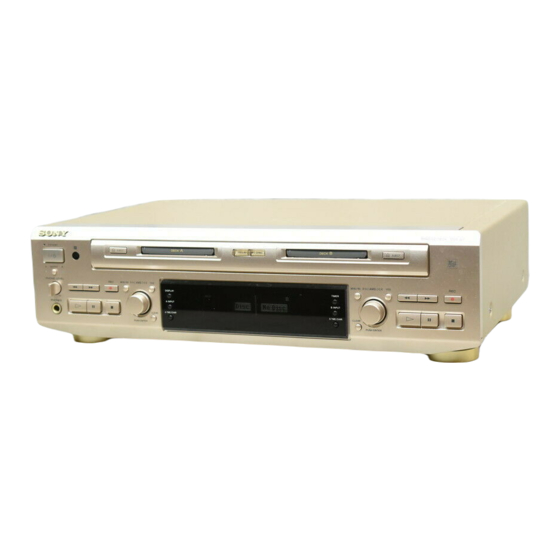
- Page 1 MDS-W1 SERVICE MANUAL AEP Model Model Name Using Similar Mechanism MDS-JE520 MD Mechanism Type MDM-5B Optical Pick-up Type KMS-260A/J1N SPECIFICATIONS — Continued on next page — MINIDISC DECK MICROFILM – 1 –...
- Page 2 SELF-DIAGNOSIS FUNCTION The self-diagnosis function consists of error codes for customers which are displayed automatically when errors occur, and error codes which show the error history in the test mode during servicing. For details on how to view error codes for the customer, refer to the following box in the instruction manual.
- Page 3 ITEMS OF ERROR HISTORY MODE ITEMS AND CONTENTS Selecting the Test Mode Display Details of History Displays the recording time. total rec Displayed as “rππππππh”. The displayed time is the total time the laser is set to the high power state. This is about 1/4 of the actual recording time.
- Page 4 WITH MARK ! ON THE SCHEMATIC DIAGRAMS AND IN THE PARTS LIST ARE CRITICAL TO SAFE OPERATION. REPLACE THESE COMPONENTS WITH SONY PARTS WHOSE PART NUMBERS APPEAR AS SHOWN IN THIS MANUAL OR IN SUPPLEMENTS PUBLISHED BY SONY. – 4 –...
-
Page 5: Table Of Contents
TABLE OF CONTENTS 1. SERVICING NOTE ............6 2. GENERAL ................ 11 3. DISASSEMBLY 3-1. Front Panel ................. 35 3-2. Slider (Cam) ................ 35 3-3. Base Unit (MBU-5B) and BD Board ........36 3-4. SW Board and Loading Motor (M103) ......36 4. -
Page 6: Servicing Note
SECTION 1 SERVICING NOTE JIG FOR CHECKING BD BOARD WAVEFORM The special jig (J-2501-149-A) is useful for checking the waveform of the BD board. The names of terminals and the checking items to be performed are shown as follows. GND : Ground I+3V : For measuring IOP (Check the deterioration of the optical pick-up laser) IOP : For measuring IOP (Check the deterioration of the optical pick-up laser) TEO : TRK error signal (Traverse adjustment) - Page 7 IOP DATA RECORDING AND DISPLAY WHEN PICKUP AND NON-VOLATILE MEMORY (IC171 OF BD BOARD) ARE REPLACED The IOP value labeled on the pick-up can be recorded in the non-volatile memory. By recording the value, it will eliminate the need to look at the value on the label of the optical pick-up.
- Page 8 CHECKS PRIOR TO PARTS REPLACEMENT AND ADJUSTMENTS Before performing repairs, perform the following checks to determine the faulty locations up to a certain extent. Details of the procedures are described in “5 Electrical Adjustments”. Criteria for Determination Measure if unsatisfactory: (Unsatisfactory if specified value is not satisfied) Laser power check •...
- Page 9 RETRY CAUSE DISPLAY MODE • In this test mode, the causes for retry of the unit during recording can be displayed on the fluorescent indicator tube. During playback, the “track mode” for obtaining track information will be set. This is useful for locating the faulty part of the unit. •...
- Page 10 Reading the Retry Cause Display Lower Bits Higher Bits Hexa- Hexadecimal Cause of Retry Occurring conditions decimal b7 b6 b5 b4 b3 b2 b1 b0 Binary shock When track jump (shock) is detected When ADER was counted more than five times ader5 continuously Discontinuous address...
-
Page 11: General
SECTION 2 GENERAL Front Panel Location of Parts and Controls 1 OUTPUT button and A. B indicator 20 B TIME/CHAR button 2 STANDBY indicator 21 B INPUT button 3 1/u (Power) button 22 TIMER button 4 Remote sensor 23 Display window 5 §... -
Page 35: Disassembly
SECTION 3 DISASSEMBLY Note: Follow the disassembly procedure in the numerical order given. 3-1. FRONT PANEL 3 Two screws (BVTT3x8) 1 Two screws (M3x8) 4 Cover 8 Flat type wire 7 Flat type wire (22core, CN811) 2 Two screws (M3x8) (17core, CN821) 9 Connector (CN551) -
Page 36: Base Unit (Mbu-5B) And Bd Board
3-3. BASE UNIT (MBU-5B) AND BD BOARD 2 Base unit (MBU-5B) 5 Flexible board (CN104) 6 Flexible board (CN101) 1 Three screws (BTP2.6x6) 3 Remove the solder (Five portion) 7 BD board 4 Screw (M1.7x4) 3-4. SW BOARD AND LOADING MOTOR (M103) 1 Screw (PTPWH M2.6x6) 2 Gear B 3 Two screws... -
Page 37: Test Mode
SECTION 4 TEST MODE 4-1. PRECAUTIONS FOR USE OF TEST MODE • As loading related operations will be performed regardless of the test mode operations being performed, be sure to check that the disc is stopped before setting and removing it. Even if the §EJECT button is pressed while the disc is rotating during continuous playback, continuous recording, etc., the disc will not stop rotating. - Page 38 4-5. SELECTING THE TEST MODE There are 31 types of test modes as shown below. The groups can be switched by rotating the AMS knob. After selecting the group to be used, press the YES button. After setting a certain group, rotating the AMS knob switches between these modes. Refer to “Group”...
- Page 39 4-5-1. Operating the Continuous Playback Mode 1. Entering the continuous playback mode 1 Set the disc in the unit. (Whichever recordable discs or discs for playback only are available.) 2 Rotate the AMS knob and display “CPLAY MODE” (S: 30). 3 Press the YES button to change the display to “CPLAY MID”.
- Page 40 4-7. TEST MODE DISPLAYS Each time the LEVEL/DISPLAY/CHAR button is pressed, the display changes in the following order. 1. Mode display Displays “TEMP ADJUST”, “CPLAYMODE”, etc. Mode display 2. Error rate display Error rate display Displays the error rate in the following way. AD = Address display C = Indicates the C1 error.
-
Page 41: Electrical Adjustments
SECTION 5 ELECTRICAL ADJUSTMENTS 5-1. PARTS REPLACEMENT AND ADJUSTMENT • Check and adjust the MDM and MBU as follows. The procedure changes according to the part replaced • Abbreviation : Optical pick-up OWH: Overwrite head • Temperature compensation offset check •... - Page 42 5-2. PRECAUTIONS FOR CHECKING LASER DIODE 4) Use the following tools and measuring devices. • Check Disc (MD) TDYS-1 EMISSINON (Parts No. 4-963-646-01) To check the emission of the laser diode during adjustments, never • TEST DISK (MDW-74/AU-1) (Parts No. 8-892-341-41) view directly from the top as this may lose your eye-sight.
- Page 43 5-6. CHECKS PRIOR TO REPAIRS Note 1: After step 4, each time the YES button is pressed, the display will be switched between “LD 0.7 mW $ ”, “LD These checks are performed before replacing parts according to 6.2 mW $ ”, and “LD Wp ”.
- Page 44 10. Observe the waveform of the oscilloscope, and check that the 5-6-4. Focus Bias Check specified value is satisfied. Do not rotate the AMS knob. Change the focus bias and check the focus tolerance amount. Checking Procedure : (Traverse Waveform) 1.
- Page 45 5-7. INITIAL SETTING OF ADJUSTMENT VALUE 5-9. TEMPERATURE COMPENSATION OFFSET ADJUTMENT Note: Save the temperature data at that time in the non-volatile memory Mode which sets the adjustment results recorded in the non-volatile as 25 ˚C reference data. memory to the initial setting value. However the results of the Note : temperature compensation offset adjustment will not change to the 1.
- Page 46 5-11. TRAVERSE ADJUSTMENT 7. Then, rotate the AMS knob and display “LDPWR CHECK” (S: 2). Connection : 8. Press the YES button once and display “LD 0.9 mW $ ”. Oscilloscope Check that the reading of the laser power meter become 0.85 to 0.91 mW.
- Page 47 5-12. FOCUS BIAS ADJUSTMENT 11. Rotate the AMS knob until the waveform of the oscilloscope moves closer to the specified value. Adjusting Procedure : In this adjustment, waveform varies at intervals of approx. 2%. 1. Load a test disk (MDW-74/AU-1). Adjust the waveform so that the specified value is satisfied as 2.
- Page 48 5-13. ERROR RATE CHECK 5-15. AUTO GAIN CONTROL OUTPUT LEVEL 5-13-1. CD Error Rate Check ADJUSTMENT Checking Procedure : Be sure to perform this adjustment when the pickup is replaced. 1. Load a check disc (MD) TDYS-1. If the adjustment results becomes “Adjust NG!”, the pickup may be 2.
- Page 49 5-15. ADJUSTING POINTS AND CONNECTING POINTS [BD BOARD] (SIDE A) CN101 D101 CN110 I+3V NOTE IC171 [BD BOARD] (SIDE B) IC101 IC121 IC192 NOTE:It is useful to use the jig. for checking the waveform. (Refer to Servicing Note on page 6.) –...
-
Page 50: Diagrams
SECTION 6 DIAGRAMS 6-1. CIRCUIT BOARDS LOCATION SW board AC board (DECK A) TRANS board POWER board KEY-A board MAIN board HP board BD board (DECK A) JACK board SEQ board BD board (DECK B) KEY-B board SW board (DECK B) –... -
Page 51: Block Diagrams
MDS-W1 DIGITAL SERVO SIGNAL PROCESSOR, DIGITAL SIGNAL PROCESSOR 6-2. BLOCK DIAGRAMS EFM/ACIRC ENCODER/DECODER, SHOCK-PROOF MEMORY CONTROLLER, ATRAC ENCODER/DECODER – BD SECTION – IC121 OVER WRITE HEAD DRIVE IC181 • Deck B is omitted. DADTI HR901 (From Deck B) • Signal path... -
Page 52: Input/Output Section
MDS-W1 – INPUT/OUTPUT SECTION – DIGITAL OUTPUT SELECTOR IC521 DOUT DINO B-DECK CLK SW DOUT IC316 IC321 (DECK A) BCKI IC321 (DECK B) FS DIVIDER 512/256FS SEL IC306 IC311 LRCK IC491 (DECK A) DIGITAL LRCKI OPTICAL IC321 INPUT (DECK B) -
Page 53: Control Section
MDS-W1 – CONTROL SECTION – IC701 • R -ch is omitted. SYSTEM • DECK B is omitted. CONTROL (DECK A) XIN-T X801 32KHz JOGA-0 XOUT-T SENS SENS XOUT X701 JOGA-1 MNT1 SHCK (MNT1) 7MHz XOUT DIG-RST DIG-RST JOGB-0 X802 MNT2... -
Page 54: Power Section
MDS-W1 – POWER SECTION – A MUTE POWER TRANSFORMER CONTROL TR201 SECTION A MUTE (Page 55) A MUTE CONTROL Q103,D110,113,114 INPUT/OUTPUT A+6V SWITCHING REG SECTION IC101 (Page 53) A-6V +6VREG IC161 RECT DIG+3.3V D161,162 +5VREG Q104 171,172 -6VREG SYS+3.3V +3.3VREG... - Page 55 MDS-W1 WAVEFORMS THIS NOTE IS COMMON FOR PRINTED WIRING BOARDS AND SCHEMATIC DIAGRAMS. • BD BOARD (1/2) • MAIN BOARD (In addition to this, the necessary note is printed in each block.) For schematic diagrams. 0.46Vp-p Note: 3.4Vp-p 5.5Vp-p • All capacitors are in µF unless otherwise noted. pF: µµF...
-
Page 56: Printed Wiring Board - Bd Section
MDS-W1 6-3. PRINTED WIRING BOARD – BD SECTION – • See page 50 for Circuit Boards Location. • Semiconductor Location Ref. No. Location • Semiconductor Location IC101 IC121 Ref. No. Location IC123 IC124 D101 IC152 D181 IC181 D183 IC192 IC103... -
Page 57: Schematic Diagram - Bd (1/2) Section
MDS-W1 6-4. SCHEMATIC DIAGRAM – BD (1/2) SECTION – • See page 60 for Waveforms. • See page 101 for IC Block Diagrams. • See page 105 for IC Pin Functions. – 63 – – 64 –... -
Page 58: Schematic Diagram - Bd (2/2) Section
MDS-W1 6-5. SCHEMATIC DIAGRAM – BD (2/2) SECTION – • See page 60 for Waveforms. • See page 61 Printed Wiring Board. • See page 102 for IC Block Diagrams. • See page 106 for IC Pin Functions. – 66 –... -
Page 59: Schematic Diagram - Jack (1/2) Section
MDS-W1 6-6. SCHEMATIC DIAGRAM – JACK (1/2) SECTION – • See page 71 Printed Wiring Board. – 67 – – 68 –... -
Page 60: Schematic Diagram - Jack (2/2) Section
MDS-W1 6-7. SCHEMATIC DIAGRAM – JACK (2/2) SECTION – • See page 103 for IC Block Diagrams. – 69 – – 70 –... -
Page 61: Printed Wiring Board - Jack Section
MDS-W1 6-8. PRINTED WIRING BOARD – JACK SECTION – • Semiconductor Location • See page 50 for Circuit Boards Location. Ref. No. Location IC301 IC311 IC321 IC331 IC371 IC381 IC411 IC421 IC481 IC485 IC491 IC501 Q301 Q302 Q303 Q304 Q321... - Page 62 MDS-W1 6-9. PRINTED WIRING BOARD – MAIN SECTION – • See page 50 for Circuit Boards Location. • Semiconductor Location Ref. No. Location IC701 IC801 IC851 IC861 IC891 IC901 IC951 Q461 Q851 Q951 – 74 – – 73 –...
-
Page 63: Printed Wiring Board - Main Section
MDS-W1 PRINTED WIRING BOARD – MAIN SECTION – • See page 50 for Circuit Boards Location. • Semiconductor Location Ref. No. Location D441 D-10 D442 D443 D-10 D444 D801 D802 D871 D872 IC301 IC306 IC311 IC316 IC321 IC331 IC351 IC441... -
Page 64: Schematic Diagram - Main (1/5) Section
MDS-W1 6-10. SCHEMATIC DIAGRAM – MAIN (1/5) SECTION – • See page 60 for Waveforms. • See page 73 Printed Wiring Board. • See page 104 for IC Block Diagrams. • See page 109 for IC Pin Functions. – 78 –... -
Page 65: Schematic Diagram - Main (2/5) Section
MDS-W1 6-11. SCHEMATIC DIAGRAM – MAIN (2/5) SECTION – • See page 60 for Waveforms. • See page 73 Printed Wiring Board. • See page 103 for IC Block Diagrams. • See page 111 for IC Pin Functions. – 79 –... -
Page 66: Schematic Diagram - Main (3/5) Section
MDS-W1 6-12. SCHEMATIC DIAGRAM – MAIN (3/5) SECTION – • See page 60 for Waveforms. • See page 75 Printed Wiring Board. • See page 104 for IC Block Diagrams. • See page 113 for IC Pin Functions. – 82 –... -
Page 67: Schematic Diagram - Main (4/5) Section
MDS-W1 6-13. SCHEMATIC DIAGRAM – MAIN (4/5) SECTION – • See page 60 for Waveforms. • See page 103 for IC Block Diagrams. • See page 75 Printed Wiring Board. – 83 – – 84 –... -
Page 68: Schematic Diagram - Main (5/5) Section
MDS-W1 6-14. SCHEMATIC DIAGRAM – MAIN (5/5) SECTION – • See page 60 for Waveforms. • See page 75 Printed Wiring Board. • See page 103 for IC Block Diagrams. – 85 – – 86 –... -
Page 69: Schematic Diagram - Bd Switch Section
MDS-W1 6-15. SCHEMATIC DIAGRAM – BD SWITCH SECTION – (Page 73, 74) 6-16. PRINTED WIRING BOARD – BD SWITCH SECTION – • See page 50 for Circuit Boards Location. (Page 73, 74) – 87 –... -
Page 70: Printed Wiring Board - Panel Section
MDS-W1 6-17. PRINTED WIRING BOARD – PANEL SECTION – • See page 50 for Circuit Boards Location. – 89 – – 90 –... -
Page 71: Schematic Diagram - Panel Section
MDS-W1 6-18. SCHEMATIC DIAGRAM – PANEL SECTION – – 91 – – 92 –... -
Page 72: Printed Wiring Board - Power Section
MDS-W1 6-19. PRINTED WIRING BOARD – POWER SECTION – • See page 50 for Circuit Boards Location. • Semiconductor Location Ref. No. Location D101 D102 D103 D104 D105 D106 D107 D108 D109 D110 D111 D112 D113 D114 D131 D141 D151... -
Page 73: Schematic Diagram - Power Section
MDS-W1 6-20. SCHEMATIC DIAGRAM – POWER SECTION – • See page 103 for IC Block Diagrams. – 95 – – 96 –... -
Page 74: Printed Wiring Board - Trans Section
MDS-W1 6-21. PRINTED WIRING BOARD – TRANS SECTION – • See page 50 for Circuit Boards Location. – 97 – – 98 –... -
Page 75: Schematic Diagram - Trans Section
MDS-W1 6-22. SCHEMATIC DIAGRAM – TRANS SECTION – – 99 – – 100 –... -
Page 76: Ic Block Diagrams
6-23. IC BLOCK DIAGRAMS IC121 CXD2654R • BD section IC101 CXA2523AR 100 99 98 97 96 95 94 93 92 91 90 89 88 87 86 85 84 83 82 81 80 79 78 77 76 SPINDLE GENERATOR SERVO 75 TE 43 42 MNT0 74 SE... -
Page 77: Main Section
• Jack (2/2) section IC311, 316, 521 SN74HC157APW-E20 IC501 SN74HCU04AN STROEE • Main section SELECT IC301 SN74HCU04APW-E20 IC331, 351 AK4321-VF-E2 19 18 17 16 15 SERIAL INPUT INTERFACE ∆Σ 8 × MODULATOR INTERPOLATOR IC306 SN74HC74APW-E20 ∆Σ 8 × MODULATOR INTERPOLATOR CLOCK OSC/DIVIDER DE-EMPHASIS CONTROL... - Page 78 IC471, 831 SN74LVC125APW-E20 IC751, 951 LB1830M-S-TE-L VREF VCONT 1 OE 14 VCC VREF 4 OE LOGIC PREDRIVER 2 OE 3 OE OUT2 OUT1 VS IC991 TC4W53FU-TE12L IC491 TC7W74FU (TE12R) • Power section IC101 LA5632 IC511, 516 SN74HC153APW-E20 – DATA INPUTS STBY STROBE OUTPUT...
-
Page 79: Ic Pin Functions
6-24. IC PIN FUNCTIONS • IC101 RF Amplifier (CXA2523AR) Pin No. Pin Name Function I-V converted RF signal I input I-V converted RF signal J input Middle point voltage (+1.5V) generation output 4 to 9 A to F Signal input from the optical pick-up detector Light amount monitor input Laser APC output APCREF... - Page 80 • IC121 Digital Signal Processor, Digital Servo Signal Processor, EFM/ACIRC Encoder/Decoder, Shock-proof Memory Controller, ATRAC Encoder/Decoder, 2M Bit DRAM (CXD2654R) Pin No. Pin Name Function FOK signal output to the system control (monitor output) MNT0 (FOK) “H” is output when focus is on MNT1 (SHCK) Track jump detection signal output to the system control (monitor output) MNT2 (XBUSY)
- Page 81 Pin No. Pin Name Function Data input/output for DRAM 50, 51 D2, D3 MVCI I (S) Clock input from an external VCO (Fixed at “L”) ASYO Playback EFM duplex signal output ASYI I (A) Playback EFM comparator slice level input AVDD —...
- Page 82 Pin No. Pin Name Function Tracking servo drive PWM output (+) TFDR — +3V power supply (Digital) DVDD Focus servo drive PWM output (+) FFDR Focus servo drive PWM output (–) FRDR 176.4 kHz clock signal output (X’tal) (Not used) Sled servo drive PWM output (–) SRDR Sled servo drive PWM output (+)
- Page 83 • IC701 (DECK A) System Control (M30610MCA-254FP) Pin No. Pin Name Function 1, 2 — DA OUT0 Not used DA OUT1 SQSY ATP address sync or subcode Q sync input from CXD2654R — Not used — Not used BYTE Input switched by data bus (Connected to ground) CNVSS —...
- Page 84 Pin No. Pin Name Function Loading motor control output LD-OUT Loading motor voltage control output LD-LOW Loading motor control output LD-IN Not used — Detection signal input from the recording position detection switch REC. P Detection signal input from the playback position detection switch PB.
- Page 85 • IC801 Master Control (M30612MAA-202FP) Pin No. Pin Name Function — Not used REMOCOM Remote controller Sircs input — Not used BYTE Data bus switching signal input CNVSS — Ground XIN-T Clock input (32 kHz) XOUT-T Clock output (32 kHz) SYSTEM-RESET System reset signal input “L”:Reset XOUT...
- Page 86 Pin No. Pin Name Function Fluorescent display tube module data output 65-72 DISPLAY D7-D0 — Not used 73-76 — MD SYNC LED output LED3 (MD SYNC) SEQUENCE LED output LED2 (SEQUENCE) OUTPUT LED output LED0 (MONITOR) POWER LED output LED1 (POWER) 81-88 —...
- Page 87 • IC901 (DECK B) System Control (M30610MCA-254FP) Pin No. Pin Name Function 1, 2 — DA OUT0 Not used DA OUT1 SQSY ATP address sync or subcode Q sync input from CXD2654R — Not used — Not used BYTE Input switched by data bus (Connected to ground) —...
- Page 88 Pin No. Pin Name Function Loading motor control output LD-OUT Loading motor voltage control output LD-LOW Loading motor control output LD-IN Not used — Detection signal input from the recording position detection switch REC. P Detection signal input from the playback position detection switch PB.
-
Page 89: Exploded Views
SECTION 7 EXPLODED VIEWS NOTE: The components identified by • Items marked “*” are not stocked since they are mark ! or dotted line with mark seldom required for routine service. Some delay ! are critical for safety. should be anticipated when ordering these items. Replace only with part number •... -
Page 90: Front Panel Section
* 68 1-668-304-11 HP BOARD 3-354-981-01 SPRING (SUS), RING X-4949-906-1 ESCUTCHEON ASSY 4-900-235-01 PLATE, INDICATION 4-996-690-71 LID (CARTRIDGE) 4-996-698-61 EMBLEM, SONY 4-999-360-11 PANEL, FRONT 4-996-690-81 LID (CARTRIDGE) 4-951-620-01 SCREW (2.6X8), +BVTP 4-996-683-21 BUTTON (POWER) 4-976-593-01 SPRING (LID), TORSION * 57... -
Page 91: Chassis Section
7-3. CHASSIS SECTION not supplied TR201 not supplied not supplied The components identified by mark ! or dotted line with mark ! are critical for safety. Replace only with part number specified. Ref. No. Part No. Description Remark Ref. No. Part No. -
Page 92: Mechanism Deck Section (Mdm-5B)
7-4. MECHANISM DECK SECTION (MDM-5B) M103 MBU-5A Ref. No. Part No. Description Remark Ref. No. Part No. Description Remark * 201 1-668-111-11 SW BOARD 4-996-227-01 LEVER (HEAD) * 202 4-996-217-01 CHASSIS 4-996-223-01 INSULATOR (F)(BLACK) 4-996-229-01 SPRING (HEAD LEVER), TORSION * 204 4-996-218-01 BRACKET (GUIDE R) 4-996-212-01 LEVER (LIMITTER) 4-996-277-01 SPRING (O/C), TENSION... -
Page 93: Base Unit Section (Mbu-5B)
7-5. BASE UNIT SECTION (MBU-5B) HR901 not supplied not supplied M101 S102 M102 The components identified by mark ! or dotted line with mark ! are critical for safety. Replace only with part number specified. Ref. No. Part No. Description Remark Ref. -
Page 94: Electrical Parts List
SECTION 8 ELECTRICAL PARTS LIST Note: • Due to standardization, replacements in the parts list • SEMICONDUCTORS The components identified by In each case, u: µ , for example: may be different from the parts specified in the mark ! or dotted line with mark uA...: µ... - Page 95 Ref. No. Part No. Description Remark Ref. No. Part No. Description Remark C144 1-163-251-11 CERAMIC CHIP 100PF L151 1-412-029-11 INDUCTOR CHIP 10uH C146 1-163-038-91 CERAMIC CHIP 0.1uF L152 1-412-029-11 INDUCTOR CHIP 10uH L153 1-412-032-11 INDUCTOR CHIP 100uH C151 1-126-206-11 ELECT CHIP 100uF 6.3V C152...
- Page 96 JACK Ref. No. Part No. Description Remark Ref. No. Part No. Description Remark R151 1-216-073-00 METAL CHIP 1/10W < RESISTOR > R152 1-216-073-00 METAL CHIP 1/10W R551 1-249-429-11 CARBON 1/4W R158 1-216-097-91 RES,CHIP 100K 1/10W R552 1-249-429-11 CARBON 1/4W R159 1-216-097-91 RES,CHIP 100K 1/10W...
- Page 97 JACK Ref. No. Part No. Description Remark Ref. No. Part No. Description Remark C392 1-126-022-11 ELECT 47uF Q391 8-729-141-30 TRANSISTOR 2SC3623A-LK C393 1-126-022-11 ELECT 47uF Q392 8-729-141-30 TRANSISTOR 2SC3623A-LK C394 1-126-022-11 ELECT 47uF Q393 8-729-141-30 TRANSISTOR 2SC3623A-LK C395 1-126-022-11 ELECT 47uF Q394 8-729-141-30 TRANSISTOR 2SC3623A-LK...
- Page 98 KEY-A JACK Ref. No. Part No. Description Remark Ref. No. Part No. Description Remark R384 1-215-424-00 METAL 1.3K 1/4W A-4724-103-A KEY-A BOARD, COMPLETE R385 1-215-424-00 METAL 1.3K 1/4W ********************* R386 1-215-424-00 METAL 1.3K 1/4W R387 1-259-484-11 CARBON 220K 1/6W 3-362-478-01 HOLDER (T), LED R388 1-259-484-11 CARBON 220K...
- Page 99 KEY-A KEY-B MAIN Ref. No. Part No. Description Remark Ref. No. Part No. Description Remark S634 1-762-875-21 SWITCH, KEYBOARD (0 (DECK A)) C305 1-414-235-11 INDUCTOR CHIP 0uH S635 1-762-875-21 SWITCH, KEYBOARD () (DECK A)) C306 1-163-038-91 CERAMIC CHIP 0.1uF C307 1-163-275-11 CERAMIC CHIP 0.001uF 1-762-875-21 SWITCH, KEYBOARD (REC r (DECK A))
- Page 100 MAIN Ref. No. Part No. Description Remark Ref. No. Part No. Description Remark C446 1-163-038-91 CERAMIC CHIP 0.1uF C807 1-163-251-11 CERAMIC CHIP 100PF C447 1-163-038-91 CERAMIC CHIP 0.1uF C808 1-163-251-11 CERAMIC CHIP 100PF C448 1-163-038-91 CERAMIC CHIP 0.1uF C449 1-163-038-91 CERAMIC CHIP 0.1uF C809 1-163-251-11 CERAMIC CHIP...
- Page 101 MAIN Ref. No. Part No. Description Remark Ref. No. Part No. Description Remark D801 8-719-016-74 DIODE 1SS352 L513 1-500-245-11 INDUCTOR CHIP 0uH L520 1-500-245-11 INDUCTOR CHIP 0uH D802 8-719-016-74 DIODE 1SS352 L522 1-500-245-11 INDUCTOR CHIP 0uH D871 8-719-016-74 DIODE 1SS352 L524 1-500-245-11 INDUCTOR CHIP 0uH D872...
- Page 102 MAIN Ref. No. Part No. Description Remark Ref. No. Part No. Description Remark R453 1-216-667-11 METAL CHIP 4.7K 0.5% 1/10W R814 1-216-073-00 METAL CHIP 1/10W R815 1-216-073-00 METAL CHIP 1/10W R454 1-216-667-11 METAL CHIP 4.7K 0.5% 1/10W R816 1-216-073-00 METAL CHIP 1/10W R455 1-216-295-91 SHORT...
- Page 103 MAIN POWER Ref. No. Part No. Description Remark Ref. No. Part No. Description Remark R929 1-216-073-00 METAL CHIP 1/10W C144 1-126-933-11 ELECT 100uF C151 1-126-933-11 ELECT 100uF R930 1-216-073-00 METAL CHIP 1/10W R931 1-216-073-00 METAL CHIP 1/10W C152 1-162-306-11 CERAMIC 0.01uF R936 1-216-073-00 METAL CHIP...
- Page 104 MDS-W1 Ref. No. Part No. Description Remark Ref. No. Part No. Description Remark IC171 8-759-604-94 IC M5F79M06L MISCELLANEOUS IC191 8-759-604-86 IC M5F7807L ************* < TRANSISTOR > 1-783-177-11 WIRE (FLAT TYPE) (27 CORE) 1-783-176-11 WIRE (FLAT TYPE) (23 CORE) Q103 8-729-422-57 TRANSISTOR UN4111...
Need help?
Do you have a question about the MDS-W1 and is the answer not in the manual?
Questions and answers