Table of Contents
Advertisement
Quick Links
Download this manual
See also:
Instruction Manual
MODEL
STANDBY/ON
DISPLAY
PLAY MODE
STANDBY
POWER
DIMMER
CLEAR
ON
OFF
Black, Silver and Golden models
BMDD1N, BMDC1N
BMUP2P, SMUP2P
BMUS4P, BMUT3P,
GMUK3P, GMUR6P,
GMUT3P, SMUS4P
SAFETY-RELATED COMPONENT
WARNING!!
COMPONENTS IDENTIFIED BY MARK
SCHEMATIC DIAGRAM AND IN THE PARTS LIST ARE
CRITICAL FOR RISK OF FIRE AND ELECTRIC SHOCK.
REPLACE THESE COMPONENTS WITH ONKYO
PARTS WHOSE PART NUMBERS APPEAR AS SHOWN
IN THIS MANUAL.
MAKE LEAKAGE-CURRENT OR RESISTANCE
MEASUREMENTS TO DETERMINE THAT EXPOSED
PARTS ARE ACCEPTABLY INSULATED FROM THE
SUPPLY CIRCUIT BEFORE RETURNING THE
APPLIANCE TO THE CUSTOMER.
SERVICE MANUAL
SERVICE MANUAL
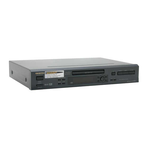
DVD PLAYER
DV-SP501
TOP MENU
MENU
RETURN
SETUP
120V AC, 60Hz
230-240V AC, 50Hz
110-240V AC, 50/60Hz
Ref. No. 3766
ON
STANDBY
OPEN/
CLOSE
REPEAT
A-B
RANDOM
PLAY MODE
1
2
3
DISPLAY
4
5
6
DIMMER
7
8
9
0
CLEAR
TOP MENU
MENU
ENTER
RETURN
SETUP
PAUSE
STOP
PLAY
AUDIO
ANGLE SUBTITLE ZOOM
TV CONTROL
TV/VIDEO
CHANNEL
ON/
STANDBY
VOLUME
RC-524DV
RC-524DV
North American model
ON THE
DV-SP501
072003
ON
STANDBY
OPEN/
CLOSE
REPEAT
A-B
RANDOM
PLAY MODE
1
2
3
DISPLAY
4
5
6
DIMMER
7
8
9
0
CLEAR
TOP MENU
MENU
ENTER
RETURN
SETUP
AUDIO
ANGLE SUBTITLE ZOOM
RC-523DV
RC-523DV
Other models
Advertisement
Table of Contents

Related Manuals for Onkyo DV-SP501


Summary of Contents for Onkyo DV-SP501
-
Page 1: Dvd Player
COMPONENTS IDENTIFIED BY MARK ON THE SCHEMATIC DIAGRAM AND IN THE PARTS LIST ARE CRITICAL FOR RISK OF FIRE AND ELECTRIC SHOCK. REPLACE THESE COMPONENTS WITH ONKYO PARTS WHOSE PART NUMBERS APPEAR AS SHOWN IN THIS MANUAL. MAKE LEAKAGE-CURRENT OR RESISTANCE... -
Page 2: Other
DV-SP501 SPECIFICATIONS North American model: Standard NTSC Video system Other models: PAL/AUTO North American model: 1, European model: 2, Region code Australian and South American models: 4, Asian model: 3, Chinese model: 6 Laser Semiconductor laser, wavelength 650 nm (DVD), 780 nm (CD) 4 HzÐ20 kHz @ 48 kHz sampling rate... -
Page 3: Protection Of Eyes From Laser Beam During Servicing
DV-SP501 SERVICE PROCEDURES-1 PROTECTION OF EYES FROM LASER BEAM DURING SERVICING This set employs a laser. Therefore, be sure to follow carefully the instructions below when servicing. Laser Diode Properties WARNING!! Wavelength: 650/780nm (DVD/CD) SERVICE WARNING : DO NOT APPROACH THE LASER EXIT WITH THE EYE TOO CLOSELY. - Page 4 DV-SP501 SERVICE PROCEDURES-2 2. Safety-check out (Only U.S.A. model) After correcting the original service problem perform the following safety check before releasing the set to the customer Connect the insulating-resistance tester between the plug of power supply cord and terminal GND on the back panel.
- Page 5 DV-SP501 EXPLODED VIEW A11a P910 P702 A11a P502 P501 P503 P701 A27 x 3 Z91A S731 P901A P910...
- Page 6 DV-SP501 EXPLODED VIEW TRAVERSE MECHANISM 15 (Torque : 0.15 +/- 0.01 N•m) Silicone Adhesive GEM1037 DVDM CN101 (Pickup Assy) 4 (Adjustment screw) Silicone Adhesive GEM1037 Screw Tight 15 (Torque : 0.15 +/- 0.01 N•m) GYL1001 (Adjustment spring) To DVDM CN102...
- Page 7 DV-SP501 EXPLODED VIEW / PARTS LIST LOADING MECHANISM Note : Refer to Refer to "2.5 TRAVERSE MECHA. ASSY-S". " Application of Lubricant". To DVDM CN101 (Pickup Assy-S) To DVDM CN104 (Stepping Motor) Daifree To DVDM CN102 (Spindle Motor) GEM1036 Lubricating Oil...
-
Page 8: Vsel1
DV-SP501 P201 Q351 JFJ3000 C221 R221 R231 OPTICAL_OUT P292A 470/6.3 L201 C360 P/XI R224 ASPECT R232 104Z C222 104K R222 L202 C223 R223 R233 L203 SIGNAL 470/6.3 P201 Except <MUP> 1000/6.3 C224 L354 BK1608LM182-T P350 1000/6.3 C225 B/CB RI_OUT P352... -
Page 9: Table Of Contents
SCHEMATIC DIAGRAM : OUTPUT TERMINAL PC BOARD NAAR-7997 OPTIC C354 -27V L351 BK1608LM182-T FLAC1 VDET C356 FLAC2 IRIN EVER+5V BK1608 DEMO SYSRESET RESET P_ON R351 C363 XSCK L352 223Z XRDY BK1608LM182-T R102 C364 VSEL1 VSEL1 223Z R103 VSEL2 VSEL2 R357 470 L353 BK1608LM182-T R104... -
Page 10: Squeeze
DV-SP501 SCHEMATIC DIAGRAM : OUTPUT TERMINAL PC BOARD NAAR-7997 P201 Q351 JFJ3000 C221 R221 R231 OPTICAL_OUT P292A 470/6.3 L201 C360 P/XI R224 ASPECT R232 C354 104Z -27V C222 104K R222 L202 L351 BK1608LM182-T FLAC1 C223 R223 R233 VDET L203 C356... -
Page 11: Letter
DV-SP501 MUP MUT/MUK MUS/MUA Region R738 R739 R740 : STANDBY SWITCH R741 PC BOARD NADIS-7999 R742 R743 R752 R753 R754 R755 R756 R757 Q705 REMSENS 1.8K 3.9K R751 2.7K STB_L STB_L C706 Q708 100/6.3 R759 R760 R761 R762 R763 R764 RN1407 1.8K... -
Page 12: Other
SCHEMATIC DIAGRAM Model Setup Integra Others : DISPLAY CIRCUIT PC BOARD NADIS-7998 R736 R737 HNV-13SS12T Q702 Q706 R725 Q707 R724 FL_ON/OFF STB_L K2 20 VDET 19 AVSS 18 VCOFF 17 42: NC4 REMO 16 IRIN 15 R708 ACK 14 NC10 DISPKLAYMODE 13 R707 SYSR... - Page 13 DV-SP501 SCHEMATIC DIAGRAM MUP MUT/MUK MUS/MUA Model Setup Region Integra Others R738 : DISPLAY CIRCUIT PC BOARD NADIS-7998 R736 R739 R737 R740 : STANDBY SWITCH R741 PC BOARD NADIS-7999 R742 R743 HNV-13SS12T Q702 R752 R753 R754 R755 R756 R757 Q705 REMSENS 1.8K...
-
Page 14: Cy/G
DV-SP501 5V Reg. (C/V) (C/V) (C/V) (PR/R) (PR/R) (PR/R) (PB/B) (PB/B) (PB/B) (CY/G) (CY/G) (CY/G) (C/V) : VIDEO SIGNAL ROUTE (C/V) : S VIDEO SIGNAL ROUTE (Y) : S VIDEO SIGNAL ROUTE (Y) (PR/R) : VIDEO SIGNAL ROUTE (PR/R) (CY/G) - Page 15 SCHEMATIC DIAGRAM DVD MAIN CIRCUIT PC BOARD (3/3) DB-VPB501/XJ 1.8V Reg. 1.8V Reg.
- Page 16 DV-SP501 SCHEMATIC DIAGRAM DVD MAIN CIRCUIT PC BOARD (3/3) DB-VPB501/XJ 1.8V Reg. 1.8V Reg. 5V Reg. (C/V) (C/V) (C/V) (PR/R) (PR/R) (PR/R) (PB/B) (PB/B) (PB/B) (CY/G) (CY/G) (CY/G) (C/V) : VIDEO SIGNAL ROUTE (C/V) : S VIDEO SIGNAL ROUTE (Y)
- Page 17 DV-SP501 : FE_DATA SIGNAL ROUTE (RF) : RF SIGNAL ROUTE (C/V) : VIDEO SIGNAL ROUTE (C/V) : S VIDEO SIGNAL ROUTE (Y) : S VIDEO SIGNAL ROUTE (C) (AD) : AUDIO DATA SIGNAL ROUTE : AUDIO SIGNAL ROUTE (DIGITAL) (DVD)
- Page 18 SCHEMATIC DIAGRAM DVD MAIN CIRCUIT PC BOARD (2/3) DB-VPB501/XJ (AD) (AD)
- Page 19 DV-SP501 SCHEMATIC DIAGRAM DVD MAIN CIRCUIT PC BOARD (2/3) DB-VPB501/XJ : FE_DATA SIGNAL ROUTE (RF) : RF SIGNAL ROUTE (C/V) : VIDEO SIGNAL ROUTE (C/V) : S VIDEO SIGNAL ROUTE (Y) : S VIDEO SIGNAL ROUTE (C) (AD) : AUDIO DATA SIGNAL ROUTE...
- Page 20 DV-SP501 (RF) : RF SIGNAL ROUTE : FOCUS SERVO LOOP LINE : TRACKING SERVO LOOP LINE : STEPPING SERVO LOOP LINE (RF) (RF) (RF)
- Page 21 SCHEMATIC DIAGRAM DVD MAIN CIRCUIT PC BOARD (1/3) CLAMP DB-VPB501/XJ UNCLAMP OPENC CLOSEC ROT DRV LOAD DRVC XDRV MUTE XDRV MUTE2 (RF) (RF) (RF) (RF) (RF) (RF)
- Page 22 DV-SP501 SCHEMATIC DIAGRAM DVD MAIN CIRCUIT PC BOARD (1/3) CLAMP DB-VPB501/XJ UNCLAMP OPENC CLOSEC (RF) : RF SIGNAL ROUTE ROT DRV : FOCUS SERVO LOOP LINE LOAD DRVC : TRACKING SERVO LOOP LINE : STEPPING SERVO LOOP LINE XDRV MUTE...
-
Page 23: Gnd2
DV-SP501 SCHEMATIC DIAGRAM U20 : POWER SUPPLY UNIT NGPS-0040-100-120V <MDD/ MDC> NGPS-0041-100-240V Except <MDD/ MDC> EV+12V C4: 250WXA68M 16x20 <MDD/MDC> P-con 400WXA68A 18x20 Wxcept <MDD/MDC> D1-D4 SJW1 VS1 C1 49101.6PAR SW+8V C30 R32 SW+8V 49101.6PAR AC-H AC-G 15 -16 PHC1... -
Page 24: Gnd4
DV-SP501 PC BOARD CONNECTION DIAGRAM DPS-5.4 ONLY P801 NAETC-8005 P851B P802 U1: OUTPUT TERMINAL PCB U5: INLET TERMINAL PCB NAAR-7997 NAPS-8001 P981A P981A P351B BROWN WHITE P982A P982B P292A P-ON P851A E+5V SW+5V SW+M8V SW+8V CN903 E+12V -27V CN902 FLAC2... - Page 25 DV-SP501 R1006 D604 D603 R1014 R1013 D605 D602 Q604 Q607 Q601 D606 Q606 Q608 R608 C602 Q601 R1011 R1015 R1017 D601 R1010 R1012 R1016 Q603 Q602 R601 R602 R603 Q605 R606...
- Page 26 PRINTED CIRCUIT BOARD FROM SOLDERING SIDE VIEW : OUTPUT TERMINAL PC BOARD NAAR-7997 C367 C360 C354 Q352 R435 Q352 Q407 Q405 Q406 C361 R1003 C903 Q463 C352 Q460 R458 R431 R119 R461 R460 D101 C901 Q403 Q404 R427 D922 R428 D921 Q402 R463...
- Page 27 DV-SP501 PRINTED CIRCUIT BOARD FROM SOLDERING SIDE VIEW : OUTPUT TERMINAL PC BOARD NAAR-7997 C367 C354 C360 R1006 Q352 R435 Q352 Q407 Q405 Q406 C361 R1003 Q463 C903 C352 D604 Q460 R458 R431 D603 R1014 R119 R461 R1013 D605 D602...
- Page 28 DV-SP501 P205 P203 P201 P601 P205 P201 P203 J180 J152 C221 C251 B/CB P292A J159 R/CR C223 C252 J173 J174 J160 J156 J166 J176 J162 C601 C603 J175 J164 J177 J157 CN903 J179 CN902 J178...
-
Page 29: Gnd5
C405 J139 C404 C403 C922 C401 J307 J308 J302 J112 C402 J301 P-ON E+5V SW+5V 25137997C C911 C906 SW+M8V SW+8V NCAR-7997 E+12V J142 -27V FLAC2 J304 Component side FLAC1 J104 P702B J116 P351A J143 DV-SP501 DPS-5.4 J115 CN901 J132 P701A... -
Page 30: Gnd3
DV-SP501 PRINTED CIRCUIT BOARD FROM SOLDERING SIDE VIEW : OUTPUT TERMINAL PC BOARD NAAR-7997 Q356 Q351 P352 P205 P350 P802 P401 P402 P203 P104 Q356 P802 J109 J102 P402 Q351 P350 J101 P352 P201 J108 P601 J149 P205 J128 Q801... - Page 31 DV-SP501 PRINTED CIRCUIT BOARD FROM BOTTOM VIEW : STANDBY SWITCH PC BOARD NADIS-7999 25137999 NCDIS-7999 Q708 S716 Soldering side Component side : INLET TERMINAL PC BOARD : POWER SWITCH PC BOARD NAPS-8001 NASW-8000 25138000 P981A NCSW-8000 P981A S991 WHITE BROWN...
- Page 32 DV-SP501 PRINTED CIRCUIT BOARD FROM SOLDERING SIDE VIEW : DISPLAY CIRCUIT PC BOARD NADIS-7998 P731 P702A J723 P701B J702 NCDIS-7998 25137998 C701 C706 PLAY STOP OPEN PAUSE X701 S710 S701 J724 S703 S702 PLAY_MODE DISPLAY J733 MENU TOP_MENU J715 S713...
- Page 33 PRINTED CIRCUIT BOARD FROM SOLDERING SIDE VIEW : DISPLAY CIRCUIT PC BOARD NADIS-7998 P731 P702A J723 P701B C701 PLAY STOP OPEN PAUSE X701 S710 J724 S701 S703 S702 MENU J733 TOP_MENU S706 S704 J731 SETUP RETURN J729 S707 S705 DOWN S708 J717 S709...
- Page 34 DV-SP501 J702 NCDIS-7998 25137998 C706 X701 PLAY_MODE DISPLAY J715 S713 S714 Q705 Q705 J707 J712 J713 J708 J703 J711 J709 J714 J704 J705 J706 J710 Q702 R7001 S712 S715 CLEAR DIMMER Q702 Component side Soldering side...
-
Page 35: Loab Assy
DV-SP501 PRINTED CIRCUIT BOARD VIEW LOAB ASSY SIDE A SIDE B LOAB S101 LOAD+ VWG2426- CN602 C102 CN602 LOAD- PYKC F6 VNP1910- C101 CN601 CN601 CN602 CN601 CN601 CN602 CN103 LOADING MOTOR ASSY... -
Page 36: Gnd2
DV-SP501 PRINTED CIRCUIT BOARD VIEW DVD MAIN CIRCUIT PC BOARD (DB-VPB501/XJ) SIDE A SIDE A SPINDLE STEPPING PICKUP ASSY Output terminal MOTOR MOTOR CN1013 CN601 CN901 CN105 CN104 CN101 IC421 CN101 IC601 CN104 CN105 CN901 Q726 CN121 CN122 IC701 CN921... - Page 37 DV-SP501 PRINTED CIRCUIT BOARD VIEW DVD MAIN CIRCUIT PC BOARD (DB-VPB501/XJ) SIDE B SIDE B CN931 R1011 CN111 HEAT-RESISITANCE R1012 CN941 IC603 PRE-FLAX CN911 R452 Q452 Q603 C233 C230 IC501 CN112 NORMAL SOLDER C200 R210 R200 LEAD FREE SOLDER (L210)
-
Page 38: Gnd1
DV-SP501 IC BLOCK DIAGRAM / TERMINAL DESCRIPTION Q532 : TC74VHCU04FT Hex inverter Pin layout 14 Vcc 13 6A 12 6Y 11 5A Truth table 10 5Y 9 4A 8 4Y... - Page 39 DV-SP501 IC BLOCK DIAGRAM/ TERMINAL DESCRIPTION Q601 : TC4053B TRIPLE 2 - CHANNEL MULTIPLEXER / DEMULTIPLEXER PIN LAYOUT TRUTH TABLE CONTROL INPUTS "ON" CHANNEL Y-COM INHIBIT X-COM 0X, 0Y, 0Z Z-COM 1X, 0Y, 0Z 0X, 1Y, 0Z 1X, 1Y, 0Z...
- Page 40 DV-SP501 IC BLOCK DIAGRAM / TERMINAL DESCRIPTION IC301 : STM6316ATXXA FRONT END IC Block Diagram...
-
Page 41: Gnda1
DV-SP501 IC BLOCK DIAGRAM / TERMINAL DESCRIPTION IC301 : STM6316AT R IF t i c t i c t s i t s i t s i t s i t s i i t i i t i... - Page 42 DV-SP501 IC BLOCK DIAGRAM / TERMINAL DESCRIPTION IC301 : STM6316AT t s i l l u / IF / IF i t i l l u - t l l i c y t i d l l - t l...
- Page 43 DV-SP501 IC BLOCK DIAGRAM / TERMINAL DESCRIPTION IC301 : STM6316AT l l i l l i t i c l i b y t i...
- Page 44 DV-SP501 IC BLOCK DIAGRAM / TERMINAL DESCRIPTION IC601 : STM5589CVA BACK END IC Dir. & l a i l a i . t i . t i...
- Page 45 DV-SP501 IC BLOCK DIAGRAM / TERMINAL DESCRIPTION IC601 : STM5589CVA BACK END IC Dir. t i s t i s t i s t i s t i s t i s t i s t i s t s i...
- Page 46 DV-SP501 IC BLOCK DIAGRAM / TERMINAL DESCRIPTION IC601 : STM5589CVA BACK END IC Dir. ' L ' L' ' L' ' L' ' : ' L : ' L c i t i t i c i t i t i...
- Page 47 DV-SP501 IC BLOCK DIAGRAM / TERMINAL DESCRIPTION IC601 : STM5589CVA BACK END IC Dir. r i f ' L ' ' L ' ' L ' t i r ' L ' ' L ' ' L ' L' '...
- Page 48 DV-SP501 IC BLOCK DIAGRAM / TERMINAL DESCRIPTION IC601 : STM5589CVA BACK END IC Dir. ' L ' l a i l a i...
- Page 49 DV-SP501 IC BLOCK DIAGRAM / TERMINAL DESCRIPTION IC601 : STM5589CVA BACK END IC Dir.
- Page 50 DV-SP501 IC BLOCK DIAGRAM / TERMINAL DESCRIPTION IC101 : M63018FP (BTL DRIVER)-1 Pin Arrangement Block Diagram...
- Page 51 DV-SP501 IC BLOCK DIAGRAM / TERMINAL DESCRIPTION IC101 : M63018FP (BTL DRIVER)-2 Pin Function...
- Page 52 DV-SP501 IC BLOCK DIAGRAM/ TERMINAL DESCRIPTION Q401,Q402,Q403,Q404 NJM4580M-D (2-ch Ope. amp.) Pin description 1. A OUTPUT 2. A -INPUT 3. A +INPUT 4. V- 5. B +INPUT 6. B -INPUT 7. B OUTPUT 8. V+ (Top view)
- Page 53 DV-SP501 IC BLOCK DIAGRAM/ TERMINAL DESCRIPTION Q703: S-80130CLMC-JKM VOLTAGE DETECTOR (13.0V CMOS, Active L: out) Pin Layout Detection voltage: 3.0V +/-2% Delay time: 200ms typ. Pin Description Symbol Description Top view ON/OFF switch for delay time Non-connection Voltage detection output pin Voltage input pin *1.
-
Page 54: Vdet
DV-SP501 MICROPROCESSOR TERMINAL DESCRIPTION Q701 : MPD780232GC VDD1 VLOAD VDD1 VLOAD VSS1 VSS1 VDD2 VDD2 -- > FIP20 FIP21 -- > -- > -- > FIP22 RESET -- > -- > ~RESET FIP23 -- > -- > XSCK P27/~SCK1 P30/FIP24 -- >... - Page 55 DV-SP501 MICROPROCESSOR TERMINAL DESCRIPTION PIN NAME SIGNAL DESCRIPTION 1 VDD1 VDD1 Power supply port 2 VSS1 VSS1 Ground port 3 X1 Connect to clock oscillator of main micro processor 4 X2 Connect to clock oscillator of main micro processor 5 IC...
- Page 56 DV-SP501 DISASSEMBLY DVD MECHANISM-3 Pickup Assy-S Front Side Dislodge the flexible cable for the pickup from its packaged placement. Remove the flexible cable for the pickup. Flexible cable for the pickup Bottom View Adjustment screw Adjustment screw Remove the two adjustment screws and...
- Page 57 DV-SP501 DISASSEMBLY DVD MECHANISM-4 Remove the two screws. Pickup Assy-S Note: The screws are secured with epoxy. Make sure to apply epoxy after reattaching the screws. Leaf Spring Joint Spring Silicone Adhesive GEM1037 Joint 03 Silicone Adhesive GEM1037 Arrangement of the flexible cable...
- Page 58 DV-SP501 DISASSEMBLY DVD MECHANISM-5 Arrangement of the flexible cable for the pickup : Conductive surface Note: Be sure to move the Pickup Assy-S to the innermost perimeter. Pass the flexible cable below the hook, and fold it back. Fold the flexible cable inward at the position of the reference line.
- Page 59 DV-SP501 DISASSEMBLY DVD MECHANISM-1 Bonnet 1. Remove the Bonnet by removing the six screws. How to open the Tray when the power cannot be on Insert a screwdriver (small) into the slit located at the bottom of the unit, and slide the projection of the Drive Gear in the Loading Mecha.
- Page 60 DV-SP501 DISASSEMBLY DVD MECHANISM-2 Traverse Mecha. Assy-S Flexible cable Dislodge the flexible cables from their factory for the spindle motor Front Side placement. Flexible cable Flexible cable for the pickup for the stepping motor Bottom View Traverse Mecha. Assy-S Remove the four hooks.
- Page 61 DV-SP501 Removing the Traverse Mecha. Assy-S and Pickup Assy-S Loading Mecha. Assy Remove the bridge by removing the one screw. Rear View Pull out the tray, then remove it by pressing the hook. Short-circuit two points of C and D by soldering.
- Page 62 DV-SP501 Removing the Traverse Mecha. Assy-S and Pickup Assy-S Traverse Mecha. Assy-S Flexible cable Dislodge the flexible cables from their factory for the spindle motor Front Side placement. Flexible cable Flexible cable for the pickup for the stepping motor Bottom View Remove the four hooks.
- Page 63 DV-SP501 Removing the Traverse Mecha. Assy-S and Pickup Assy-S Pickup Assy-S Note: The Pickup Assy-S can be removed without Front Side removing the Traverse Mecha. Assy-S. (shown as Step .) Dislodge the flexible cable for the pickup from its packaged placement.
- Page 64 DV-SP501 Removing the Traverse Mecha. Assy-S and Pickup Assy-S Pickup Assy-S Remove the two screws. Note: The screws are secured with epoxy. Make sure to apply epoxy after reattaching the screws. Leaf Spring Joint Spring Silicone Adhesive GEM1037 Joint 03...
- Page 65 DV-SP501 Removing the Traverse Mecha. Assy-S and Pickup Assy-S Arrangement of the flexible cable for the pickup : Conductive surface Note: Be sure to move the Pickup Assy-S to the innermost perimeter. Pass the flexible cable below the hook, and fold it back.
- Page 66 DV-SP501 FIRMWARE DOWN LOADING-1 HOME MENU Confirm the Regional code and Firmware version. 1. Connect the TV monitor to the DV-SP501. Audio Settings Video Adjust 2.Turn ON the power switch and standby switch ON. (No Disc) 3. Press the "SETUP" key on the front panel.
- Page 67 Using for Window tool 6. Connect the JIG (0J13), FFC and connection cable (RS-232C straight type). 7. Turn the power switch and standby "ON" of the DV-SP501. Writing the firmware as below. No disc condition. 8. Press the start key.
- Page 68 DV-SP501 ID NUMBER AND DATA SETTING Caution: It is necessory to enter individual ID number and ID data to each player when you repair it. Note: When previous ID number and ID data, such as a factory present ID number and ID data, are maintained, the unit enters ID Number Confirmation Mode when the above keys are pressed.
- Page 69 DV-SP501 ID NUMBER AND DATA SETTING TV monitor : ID DATA Input Mode [Player's ID Number Setting] [ Remote controller RC-484M] ID Number ? > 0 0 1 5 1 * * * * 1. Press "DVD" and "1" at the same time.
-
Page 70: Other
DV-SP501 PACKIN VIEW EXCEPT <MUP> MODEL P905 P905 North American models: Other models: RC-524DV RC-523DV P901 Tape P911 P903 P902 P906 P912 P913 P915 P907 P981... -
Page 71: Other
DV-SP501 PACKING VIEW <MUP> model only P905 P902 Tape P901 Other models: RC-523DV P911 P906 P912 P903 P915 P981 Packing of accessory... - Page 72 EXPLODED VIEW PARTS LIST ! : Safety part REF. NO. PART NAME DESCRIPTION PART NO. REMARK CHASSIS 27100425B 27175316C CUSHION 28141494 HOLDER KGLS-10RT 27190428A SCREW 3TTB+8B 838130088 A11a WASHER W3*10F(BC) 87643010 HOLDER KGLS-18RT 27190657 HOLDER KGLS-22RT 27190772 LABEL(DVD2) 29362648 CLAMP HL-18-0 27301394 F BRACKET...
- Page 73 HOLDER (ML) 27191201 HOLDER (MR) 27191202 SCREW 3SMS8W.SW+14B(BC) 801433 Z91A SCREW 4TTC+8C(BC) 830440089 Output terminal PC board assy 1H505597-1A NAAR-7997-1A <MDD> <MDC> Output terminal PC board assy NAAR-7997-1B <MUP> 1H505597-1B Output terminal PC board assy 1H505597-1C NAAR-7997-1C <MUT> <MUK> Output terminal PC board assy NAAR-7997-1D <MUS>...
- Page 74 PACKING VIEW PARTS LIST ! : Safety part REF. NO. PART NAME DESCRIPTION PART NO. REMARK <B MDD,B MDC,B MUT,B CARTON 29054056 MUS> CARTON 29054057 <B MUP> CARTON <G MUT> <G MUR> <G MUK> 29054060 CARTON 29054058 <S MUP> CARTON <S MUS>...
-
Page 75: Naar
PRINTED CIRCUIT BOARD PARTS LIST U1 : OUTPUT TERMINAL PC BOARD NAAR-7997 CIRCUIT PART NAME DESCRIPTION PART NO. REMARK C101 C-CERA C CK725F1E-104Z1 332161040R1 C221 VR C CE04W6.3V-470M(VR) 394624717 C222 C-CERA C CK725B1C-104K1 332121045R1 C223 VR C CE04W6.3V-470M(VR) 394624717 C224 VR C CE04W6.3V-1000M(VR) 394621027... - Page 76 CN901 or SOCKET NSCT-30P1741 25051954 CN901 or SOCKET NSCT-30P2227 25052330 CN902 SOCKET NSCT-11P2402 25052505 CN902 or SOCKET NSCT-11P1822 25051935 CN902 or SOCKET NSCT-11P2208 25052311 CN903 SOCKET NSCT-18P2409 25052512 CN903 or SOCKET NSCT-18P1729 25051942 CN903 or SOCKET NSCT-18P2215 25052318 D101 ZENER D UDZS5.1B 224550510R2 D101 or...
- Page 77 Q463 or RN1407 2216260R2 Q463 or KRC107S 2216340R2 Q602 KRC102S 2216190R2 <MUP> Q602 or RN1402 2214470R2 <MUP> Q603 KRC102S 2216190R2 <MUP> Q603 or RN1402 2214470R2 <MUP> Q604 KTC3875-Y 2216174R2 <MUP> Q604 or KTC3875-GR 2216175R2 <MUP> Q604 or 2SC2712-Y 2213144R2 <MUP> Q604 or 2SC2712-GR 2213145R2...
-
Page 78: R357
R232 C-CARBON R RN72K1J-000JE 435030004R1 R233 C-CARBON R RN72K1J-000JE 435030004R1 R234 C-CARBON R RN72K1J-000JE 435030004R1 Except <MUP> R235 C-CARBON R RN72K1J-000JE 435030004R1 Except <MUP> R236 C-CARBON R RN72K1J-000JE 435030004R1 Except <MUP> R351 C-CARBON R RN72K1J-000JE 435030004R1 R353 C-CARBON R RN72K1J-474JE 435034744R1 R354 C-CARBON R... - Page 79 R463 C-CARBON R RN72K1J-102JE 435031024R1 R481 NF CARBON R R25J-2.2 415470224 R482 NF CARBON R R25J-2.2 415470224 R601 C-CARBON R RN72K1J-182JE 435031824R1 <MUP> R602 C-CARBON R RN72K1J-222JE 435032224R1 <MUP> R603 C-CARBON R RN72K1J-222JE 435032224R1 <MUP> R604 C-CARBON R RN72K1J-103JE 435031034R1 <MUP>...
- Page 80 P731 or SOCKET NSCT-7P1676 25051889 P731 or SOCKET NSCT-7P2425 25052528 Q705 REMO SENS RPM7138-H9 241348 R701 C-CARBON R RN72K1J-103JE 435031034R1 R702 C-CARBON R RN72K1J-000JE 435030004R1 R703 C-CARBON R RN72K1J-101JE 435031014R1 R704 C-CARBON R RN72K1J-000JE 435030004R1 R705 C-CARBON R RN72K1J-000JE 435030004R1 R706 C-CARBON R RN72K1J-000JE...
- Page 81 S715 PUSH SW NPS-111-S681 25035718 X701 CERA LOCK CST5.00MGW 3010242 Q702A CUSHION t3*10*25 28141513 U3 : STANDBY SWITCH PC BOARD NADIS-7999 CIRCUIT PART NAME DESCRIPTION PART NO. REMARK D721 SEL4110R, LED 225290 Q708 DTC114YKA 2216470R2 Q708 or KRC107S 2216340R2 Q708 or RN1407 2216260R2 R757...
- Page 91 UR>...
- Page 92 Sales & Product Planning Div. : 2-1, Nisshin-cho, Neyagawa-shi, OSAKA 572-8540, JAPAN Tel: 072-831-8111 Fax: 072-833-5222 ONKYO U.S.A. CORPORATION 18 Park Way, Upper Saddle River, N.J. 07458, U.S.A. Tel: 201-785-2600 Fax: 201-785-2650 E-mail: onkyo@onkyousa.com ONKYO EUROPE ELECTRONICS GmbH Liegnitzerstrasse 6, 82194 Groebenzell, GERMANY Tel: +49-8142-4401-0 Fax: +49-8142-4401-555 E-mail: info@onkyo.de...
Need help?
Do you have a question about the DV-SP501 and is the answer not in the manual?
Questions and answers