Marantz UD8004 Service Manual
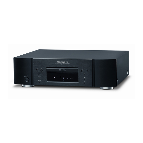
Super audio cd/blu-ray disc player
Hide thumbs
Also See for UD8004:
- User manual (69 pages) ,
- Specifications (2 pages) ,
- Specification (2 pages)
Table of Contents
Advertisement
Service
Manual
• For purposes of improvement, specifications and design are subject to change without notice.
• Please use this service manual with referring to the operating instructions without fail.
• Some illustrations using in this service manual are slightly different from the actual set.
S0306-1V02DM/DG1106
UD8004
Copyright 2011 D&M Holdings Inc. All rights reserved.
WARNING: Violators will be prosecuted to the maximum extent possible.
UD8004 /
K1B/S1B/N1B/U1B/R1B
SUPER AUDIO CD/
BLU-RAY DISC PLAYER
Ver. 2
Please refer to the
MODIFICATION NOTICE.
Advertisement
Table of Contents

Related Manuals for Marantz UD8004


Summary of Contents for Marantz UD8004
- Page 1 Service UD8004 / K1B/S1B/N1B/U1B/R1B SUPER AUDIO CD/ Manual BLU-RAY DISC PLAYER • For purposes of improvement, specifications and design are subject to change without notice. • Please use this service manual with referring to the operating instructions without fail. • Some illustrations using in this service manual are slightly different from the actual set.
- Page 2 MARANTZ Parts for your equipment are generally available to our National Marantz Subsidiary or Agent. ORDERING PARTS : Parts can be ordered either by mail or by Fax.. In both cases, the correct part number has to be specified.
-
Page 3: Service Hints And Tools
SERVICE HINTS AND TOOLS 2. SERVICE HINTS AND TOOLS SERVICE HINTS SERVICE TOOLS Audio signals disc 4822 397 30184 or TCD-784 Disc without errors + Disc with DO errors, black spots and fingerprints 4822 397 30245 (SBC444A) or TCD-726 Disc (65 min 1kHz) without no pause 4822 397 30155 Max. -
Page 4: Warning And Laser Safety Instructions
WARNING AND LASER SAFETY INSTRUCTIONS WARNING WAARSCHUWING All ICs and many other semi-conductors are Alle IC’s en vele andere halfgeleiders zijn susceptible to electrostatic discharges (ESD). gevoelig voor elektrostatische ontladingen Careless handling during repair can reduce (ESD). life drastically. Onzorgvuldig behandelen tijdens reparatie When repairing, make sure that you are kan de levensduur drastisch doen connected with the same potential as the... -
Page 5: Specifications
SPECIFICATIONS n Audio performance n General Signal format : NTSC, PAL Power supply : AC 230 V, 50/60 Hz Applicable discs /memory cards : Power consumption : (1) BD-Video discs : • When in Power Saving Standby : 0.3 W 12 cm 1 side 1 layer, 12 cm 1 side 2 layers •... -
Page 6: Wire Arrangement
WIRE ARRANGEMENT If wire bundles are untied or moved to perform adjustment or parts replacement etc., be sure to rearrange them neatly as they were originally bundled or placed afterward. Otherwise, incorrect arrangement can be a cause of noise generation. Wire arrangement viewed from the top Front Panel side Back Panel side... - Page 7 • Refer to the table below for a description of the direction in which the photos were taken. • Photographs for which no direction is indicated were taken from above the product. • The photograph is UD8004. The viewpoint of each photograph...
-
Page 8: Front Panel Assy
1. FRONT PANEL ASSY : TOP COVER → → LOADER PANEL FRONT PANEL ASSY Proceeding (1) Remove the Loadr Panel. Direction of photograph: B (2) Remove the screws. View from bottom (3) Cut the wire clampers. Disconnect the connector wire and FFC Cable. CX042 FFC Cable CY033... - Page 9 2. MAIN UNIT SUB ASSY : TOP COVER → Proceeding MAIN UNIT ASSY (1) Remove the screws. Direction of photograph: A (2) Remove the screws. Disconnect the connector wires and FFC cables. FFC Cable FFC Cable CY151 MAIN UNIT...
-
Page 10: Power Unit Assy
3. POWER UNIT ASSY : TOP COVER → POWER UNIT ASSY Proceeding (1) Remove the screws. Direction of photograph: A (2) Remove the screws. Disconnect the connector wire. CX042 CY063 CY151 CX022 CX021 CY032 POWER UNIT... - Page 11 4. AUDIO3 UNIT ASSY : TOP COVER → AUDIO3 UNIT ASSY Proceeding (1) Remove the screws. Direction of photograph: A (2) Remove the screws. Disconnect the HOCK, connector wire and FFC Cable. FFC Cable HOCK FFC Cable CX067 AUDIO3 UNIT...
- Page 12 5. AUDIO2 UNIT ASSY : TOP COVER → → AUDIO3 UNIT ASSY AUDIO2 UNIT ASSY Proceeding (1) Remove the screws. Direction of photograph: A (2) Remove the screws. Disconnect the HOCK, connector wire and FFC Cable. HOCK FFC Cable CX065 AUDIO2 UNIT ...
- Page 13 6. AUDIO UNIT ASSY : TOP COVER → → AUDIO3 UNIT ASSY AUDIO2 UNIT ASSY Proceeding → AUDIO UNIT ASSY (1) Remove the screws. Direction of photograph: A (2) Remove the screws. AUDIO UNIT (3) Remove the screws. CY022 FFC Cable...
- Page 14 7. ANALOG VIDEO UNIT ASSY : TOP COVER → → Proceeding MAIN UNIT ASSY ANALOG VIDEO UNIT ASSY (1) Remove the screws. Direction of photograph: A (2) Remove the screws. ANALOG VIDEO UNIT 8. MECHA ASSY : TOP COVER → →...
-
Page 15: Removing Discs
Removing discs : INSIDE PLATE → Proceeding SLIDE CAM (1) Remove the screws and FOOTs. View from bottom (2) Slide the SLIDE CAM in the direction of the arrow. Direction of photograph: A (3) Draw out the LOADER TRAY, then remove the disc. - Page 16 DIAGNOSTICS OF OPTICAL PICKUP AND REPLACING FE MAIN P.W.B AND BD MECHANISM UNIT ASSY s Make failure diagnostics of the Optical Pickup as follows. q If the laser drive current (Iop) becomes more than ±12[mA] of the initial value, the Optical Pickup should be replaced. The laser drive current initial value is checked by "Iop checked Method"...
- Page 17 1. Iop checked Method 1. Iop checked Method 1. Iop checked Method 1. Iop checked Method Select the laser ON/OFF(CD/DVD/BD)mode of the test mode, and check the IOP value of CD laser, DVD laser or BD Select the laser ON/OFF(CD/DVD/BD)mode of the test mode, and check the IOP value of CD laser, DVD laser or BD 1.
-
Page 18: Service Mode
SERVICE MODE 1. Heat run mode 1.1. preparation (1) Equipment used : Heat run disc (This operation may not work with any discs other than the heat run discs listed below.) : CD TEST DISC (TCD-HR01) DVD : DVD TEST DISC (TDV-HR01) : BD TEST DISC (TBD-HR01) (2) Unit setting : No spec other than the following procedure. -
Page 19: Initial Setting Mode
(1) Turn on the UD8004's power. "NO DISC" is displayed on the fl uorescent tube. (2) Press the UD8004's 1 , 5 and SOUND MODE buttons simultaneously. "INITIALIZING" is displayed on the fl uorescent tube. - Page 20 5. All Lit / All Off mode for the FL tube 5.1. preparation (1) Equipment used: None (2) Unit setting: No spec other than the following procedure. 5.2. procedure [Setting] (1) Pressing the HDMI RESOLUTION and 1 buttons for simultaneously, plug the AC cord into a power outlet. If All Lit / All Off mode is set for the FL tube, the FL tube’s display area is fully lit.
-
Page 21: Test Mode
7. Test mode 7.1. Entering the test mode The test mode is entered by pressing the 5 and 2 buttons simultaneously, plug the AC cord into a power outlet. When the test mode is set, the " 1 " and " 3 " indicators light. FL tube display when test mode entered FL Display (The display part of 13 digits) When the test mode is set, a color bar appears on the monitor. - Page 22 7.3. About each mode ・ With the mode selected, press the 1 button to set that mode. (1) Laser on/off (CD/DVD/BD) mode Press the 8 or 9 button to select [X] and press the 1 button to set it. Laser on/off control is executed and the laser current is displayed. FL Display (The display part of 13 digits) (X=1 : CD laser mode, 2 : DVD laser mode, 3 : BD(SL) laser mode, 4 : BD(DL) laser mode) (mm.mm[mA] : Stored data, nn.nn[mA] : Current value)
- Page 23 (3) Error rate measurement mode Press the 8 or 9 button to select [YY] . Refer to [Table 2 - Error rate details]. (page 22) FL Display (The display part of 13 digits) (X : measurement mode, F : Address and error rate (When not set, "F" is displayed.) Press the 1 button to begin error rate measurement.
- Page 24 (5) Track buffer output mode Press the 8 or 9 button to select "Y" and switch the track buffer output. FL Display (The display part of 13 digits) (Y=1 : Track buffer being output, 0 : Track buffer output off ) When the 2 button is pressed, the layer above the current layer is displayed.
- Page 25 7.4. Stopping the mode When the 2 button is pressed, the layer above the current layer is displayed. The relationship between the different modes and the display of the different layers is shown on the table below. Mode 1 layer 2 layer 3 layer Laser on/off (CD/DVD/BD) mode...
- Page 26 Name Address range Meaning BUF_ID_SVO_SVRAM 0x000000 ∼ 0x0005FF SVRAM T57A BUF_ID_SVO_CRAM0 0x000000 ∼ 0x0001FF CRAM0 T57B BUF_ID_SVO_CRAM1 0x000000 ∼ 0x0001FF CRAM1 T57C BUF_ID_SVO_CRAM2 0x000000 ∼ 0x0001FF CRAM2 T57D BUF_ID_SVO_CRAM3 0x000000 ∼ 0x0001FF CRAM3 T58A BUF_ID_SVO_ZRAM0 0x000000 ∼ 0x0001FF ZRAM0 T58B BUF_ID_SVO_ZRAM1 0x000000 ∼...
- Page 27 Error rate display details for each media type Measurement Remarks position The inner BIS error detection It is invalid. It is invalid. When this is selected for 2-layer DVD, circumference of signed number it shifts to YY=85. 2-layer When this is selected for 1-layer DVD or CD, it shifts to YY=73.
- Page 28 Table 3: Error log details Contents Error log No. Remarks (Error log overall layout) LD On Time (4Byte) Error type (2Byte) See "Table 3-1: Error type details" 3 (31 to 34 displayed in 4-byte units) Reserve (16Byte) Media type (2Byte) See "Table 3-2: Media type details"...
-
Page 29: Version Upgrade Procedure Of Firmware
Even with a broadband connection to the Internet, approximately about 1 hour is required for the updating procedure to be completed. Once updating starts, normal operations on the UD8004 cannot be performed until updating is completed. Also, setting items of the GUI menu of UD8004 or setting items of the image adjustment may be initialized. -
Page 30: Troubleshooting
TROUBLE SHOOTING 1. 8U-210095-7 (AUDIO UNIT)/ 8U-210094-2 (AUDIO2 UNIT)/ 8U-210094-3 (AUDIO3 UNIT) - Page 32 2. 8U-210094-1 (POWER UNIT) 2.1. The power cannot be turned on.
- Page 34 3. 8U-210095-4 (FRONT UNIT) 3.1. FL TUBE dosen't light...
- Page 35 4. 8U-310041 (MAIN UNIT) 4.1. No System Power up or Loading No Video or Audio Output...
- Page 36 4.2. No Ether-net Operation 4.3. No SD Card Operation...
- Page 37 5. 8U-210095-1 (ANALOG VIDEO UNIT) 5.1. Video/S-Video Out does not be outputted.
- Page 38 5.2. Component Out does not be outputted...
- Page 39 6. 8U-310037 (FE/SACD UNIT) 6.1. BD or DVD or CD or SACD check...
- Page 40 SEMICONDUCTORS Only major semiconductors are shown, general semiconductors etc. are omitted to list. The semiconductor which described a detailed drawing in a schematic diagram are omitted to list. 1. IC’s SII9134CTU (8U-310041 : IC502) SII9134CTU Block Diagram E-DDC CSDA DSDA Slave Master DSCL...
- Page 41 SII9134CTU Pin Function Pin # Type Description Name LVTTL Input These are the lower 12 bits of the 36-bit pixel bus. These pins are highly con- LVTTL Input figurable and support multiple RGB and YCbCr formats. See Data Bus Map- LVTTL Input pings on page 30 for complete information.
- Page 42 R5F364VDNFB (8U-310041 : IC853) R5F364VDNFB Block Diagram...
- Page 43 R5F364VDNFB Pin Function...
- Page 45 ADV7340BSTZ-3 (8U-210095-1 : IC808, IC810) 64 63 62 61 60 59 58 57 56 55 54 53 52 51 50 49 SFL/MISO DD_IO PIN 1 SET1 COMP1 DAC 1 DAC 2 ADV7340/ADV7341 DAC 3 TOP VIEW (Not to Scale) AGND DAC 4 DGND DAC 5...
- Page 46 ADV7340BSTZ-3 Pin Function Input/ Pin No. Mnemonic Output Description 13, 12, Y9 to Y0 10-Bit Pixel Port (Y9 to Y0). Y0 is the LSB. Refer to Table 31 for input modes. 9 to 2 29 to 25, C9 to C0 10-Bit Pixel Port (C9 to C0).
- Page 47 PT6302-R-001(L) (8U-210095-4 : IC101) BLOCK DIAGRAM PT6302-R-001(L) Block Diagram CGROM 248 words x 35 bits DCRAM SEGMENT 16 words x 8 bits DRIVER RSTB CGRAM 8 words x 35 bits SG35 8-BIT SHIFT CLKB REGISTER ADRAM 16 words x 2 bits DRIVER ADDRESS SELECTOR...
-
Page 48: Pin Description
PIN DESCRIPTION PT6302-R-001(L) Pin Function Pin No. Pin Name Description LQFP SSOP SG5 to SG35 1 ~ 31 9 ~ 39 Segment driver output pin SG4 to SG1 64 ~ 61 8 ~ 5 GR1 to GR16 Grid driver output pin 32 ~ 47 40 ~ 55 Power supply... - Page 49 PCM1796DBR (8U-210095-7:IC301, 8U-210094-2:IC601,IC701, 8U-210094-3:IC801,IC901) (TOP VIEW) ZEROL ZEROR AGND3L MSEL LRCK DATA AGND2 DGND AGND1 AGND3R PCM1796DBR Block Diagram I OUT L LRCK Current V OUT L Segment DATA Audio I OUT L+ Data Input I/V and Filter V COM L Oversampling Advanced Digital...
-
Page 50: Terminal Name
PCM1796DBR Pin Function TERMINAL DESCRIPTIONS DESCRIPTIONS NAME AGND1 Analog ground (internal bias) AGND2 Analog ground (internal bias) AGND3L Analog ground (L-channel DACFF) AGND3R Analog ground (R-channel DACFF) Bit clock input (1) Serial audio data input (1) DATA DGND Digital ground I OUT L+ L-channel analog current output+ I OUT L–... - Page 51 PCA9539PW,188 (8U-310041 : IC601) RESET PCA9539PW,188 Pin Function SOIC (DW), SSOP (DB), NAME DESCRIPTION QSOP (DBQ), QFN (RGE) TSSOP (PW), AND TVSOP (DGV) Interrupt output. Connect to V through a pullup resistor. Address input. Connect directly to V or ground. Active-low reset input.
- Page 52 HIN202EIBNZ-T (8U-210094-1 : IC403) HIN202EIBNZ-T Pin Function FUNCTION Power Supply Input 5V 10%, (5V 5% HIN207E). Internally generated positive supply (+10V nominal). Internally generated negative supply (-10V nominal). Ground Lead. Connect to 0V. External capacitor (+ terminal) is connected to this lead. External capacitor (- terminal) is connected to this lead.
- Page 53 2. FL DISPLAY FL TUBE (15-BT-114GNK) (8U-210095-4 : FL101)
- Page 54 --MEMO--...
-
Page 55: Block Diagram
BLOCK DIAGRAM Ethernet Common Engine Analog VIDEO PWB RJ45 MAIN PWB Internal Pulse TRANS FE SACD PWB Digtal SERVO BD / DVD / CD Decoder ETHER HUB DRIVE UNIT SATA Brige VIDEO SMSC MPEG DECORDER ENCODER S(Y/C) OUT [R8J32801AFPV] [LAN9313] BD / DVD / CD CVBS [BU19502KV-... - Page 56 PRINTED WIRING BOARDS 8U-210094 AUDIO/POWER P.W.B. UNIT(1/2) COMPONENT SIDE...
- Page 57 8U-210086 AUDIO/POWER P.W.B. UNIT(2/2) FOIL SIDE...
- Page 58 8U-210095 AUDIO POWER/VIDEO/FRONT P.W.B. UNIT(1/2) COMPONENT SIDE...
- Page 59 8U-210095 AUDIO POWER/VIDEO/FRONT P.W.B. UNIT(2/2) FOIL SIDE...
- Page 60 8U-310041 MAIN P.W.B. UNIT(1/2) COMPONENT SIDE...
- Page 61 8U-310041 MAIN P.W.B. UNIT(2/2) FOIL SIDE...
- Page 62 8U-310037 FE/SACD P.W.B. UNIT FOIL SIDE COMPONENT SIDE...
-
Page 63: Note For Parts List
NOTE FOR PARTS LIST Parts for which "nsp" is indicated on this table cannot be supplied. When ordering of part, clearly indicate "1" and "I" (i) to avoid mis-supplying. Ordering part without stating its part number can not be supplied. Part indicated with the mark "★"... -
Page 64: Parts List Of P.w.b. Unit
PARTS LIST OF P.W.B. UNIT * Parts for which "nsp" is indicated on this table cannot be supplied. * The parts listed below are for maintenance only, might differ from the parts used in the unit in appearances or dimensions. Note: The symbols in the column "Remarks"... - Page 65 Ref. No. Part No. Part Name Remarks Q'ty TR731 00MHT600121A0 KTA1268 PNP TRANSISTOR RANK=GR TR732,733 00D2730460905 KTC2875-B-RTK/P TR735 00D2730460905 KTC2875-B-RTK/P TR801-803 00MBA20035210 DTC114EU TR804-806 00MBA10026210 DTA114EU TR807,808 00D2710259903 2SA1162-GR(TE85L) TR809-812 00D2730403904 2SC2712-Y/GR(TE85L) +C TR813-816 00D2710259903 2SA1162-GR(TE85L) TR817,818 00D2730403904 2SC2712-Y/GR(TE85L) +C TR821,822 00MHT600121A0 KTA1268 PNP TRANSISTOR RANK=GR...
- Page 66 Ref. No. Part No. Part Name Remarks Q'ty RESISTORS GROUP R101 129550003504S RM73B2E115JT(HV732B) R102 129550003504S RM73B2E115JT(HV732B) R104 00D2432094064 RW99=3DR33JF R104 00D2432094077 RW99=3DR47JF N, R, S, K R108 00D2442675716 RS14B3D683JNBF (ERG) R115 00D2472035986 RM73B--332DT(1608) R116 00D2472042911 RM73B--123DT(1608) R120 00D2472034916 RM73B--561DT(1608) R130 00D2472041925 RM73B--472DT(1608) R134...
- Page 67 Ref. No. Part No. Part Name Remarks Q'ty C155 CK73B1H103KT (1608) +1608 C156 CK73B1H103KT (1608) +1608 C157 132350030504S CK73B1C225KT 1608 C158 CK73B1H102KT +1608 C159 00D2544806700 CE04W1C222MC K25(KY) C160 00D2544755903 CE04W1H560MT(KY) C161 132350030504S CK73B1C225KT 1608 C162 00D2544806700 CE04W1C222MC K25(KY) C163 132350030504S CK73B1C225KT 1608 C164 CK73F1E104ZT...
- Page 68 Ref. No. Part No. Part Name Remarks Q'ty C447 RM73B--0R0KT +1608 C449 CK73B1H102KT +1608 C450 CK73F1E104ZT +1608 C451 CK73F1E104ZT +1608 C453 00D2544722907 CE04W1H0R1MT(GR) C454 00D2544722907 CE04W1H0R1MT(GR) C455 00D2544722907 CE04W1H0R1MT(GR) C456 00D2544722907 CE04W1H0R1MT(GR) C458 CC73CH1H221JT +1608 C460 00D2544718937 CE04W1C470MT(GR) C461 CK73F1E104ZT +1608 C462 CC73CH1H221JT...
- Page 69 Ref. No. Part No. Part Name Remarks Q'ty C651 100PF J 100V APSV C652 100PF J 100V APSV C653 1000PF J 100V APSV C654 1000PF J 100V APSV C655 APSV 221J,220PF(TP) 100V PP C656 APSV 221J,220PF(TP) 100V PP C657 APSV 221J,220PF(TP) 100V PP C658 APSV 221J,220PF(TP) 100V PP C659...
- Page 70 Ref. No. Part No. Part Name Remarks Q'ty C830 APSV 471J,470PF(TP) 100V PP C831 APSV 221J,220PF(TP) 100V PP C832 00MOA227016Z0 ROS-16V 221M - H5#PE - T2 (220UF 16V) C833 APSV 221J,220PF(TP) 100V PP C834 00MOA227025R0 ROA-25V 221M -H5#PE - T2 (220UF 25V) C835 100PF J 100V APSV C836...
- Page 71 Ref. No. Part No. Part Name Remarks Q'ty OTHERS PARTS GROUP AS101 00D4170476007 RADIATOR AS102 447310014008S RADIATOR(PUE26-25) AS103 447310014015S RADIATOR(PUE26-30) CX021 2P VH CON BASE (White) CX022 2P VH CON BASE (White) CX042 4P CONN.BASE(KR-PH) CX151 15P 160mm PH-SAN CX178 17FMN-BMTTN-TFT CX211 21FMN-BMTTN-A-TFT...
- Page 72 Ref. No. Part No. Part Name Remarks Q'ty RL102 682010007608S RELAY(DQ12D1-0(M)) ST102 STYLE PIN z T101 102010016007S SW_TRANS(E3/J ST4282) z T101 102010016014S SW_TRANS(E2 ST4283) N, R, S, K z T102 101010072004S POWER TRANS(MINI/E3) z T102 101010072011S POWER TRANS(MINI/E2) N, R, S, K W101 GND TERMINAL FOR PCB W102...
- Page 73 8U-210095A AUDIO POWER/VIDEO/FRONT PWB UNIT ASSY(U model) 8U-210095C AUDIO POWER/VIDEO/FRONT PWB UNIT ASSY(N, R, S, K model) Ref. No. Part No. Part Name Remarks Q'ty SEMICONDUCTORS GROUP IC101 00D2623606902 PT6302-R-001(L) IC102 00MHW10004210 RPM6936-V4 (IR SENSOR) IC301 00D2623362903 PCM1796DBR IC302,303 00D2630896909 NJM2068MD-TE1 z IC304 00D2631227001...
- Page 74 Ref. No. Part No. Part Name Remarks Q'ty TR823 00D2710293901 2SA1022-B TR824 00D2710293901 2SA1022-B TR826 00D2710293901 2SA1022-B TR827 00D2710293901 2SA1022-B D101 00D2760401905 1SS133T77 (TAPE) D301 00MHD20002710 1D3 1A/200V D302 00MHD20002710 1D3 1A/200V D303 00MHD20002710 1D3 1A/200V D304 00MHD20003710 ! SCHOTTKY 1S100 1A 100V RECTRON D305 00MHD20003710 ! SCHOTTKY 1S100 1A 100V RECTRON...
- Page 75 Ref. No. Part No. Part Name Remarks Q'ty C113 CK73F1H103ZT +1608 C114 CK73F1E104ZT +1608 C115 CC73CH1H331JT +1608 C116 CK73F1E104ZT +1608 C117 CK73F1E104ZT +1608 C118 100UF/6.3V C119 100UF/6.3V C120 CK73F1H103ZT +1608 C301 00MOA107025R0 ROA-25V 101M -H4#PE - T2 (100UF 25V) C308 0.1UF 50V +- 5% MTFVA0050J104 C309 CK73F1E104ZT...
- Page 76 Ref. No. Part No. Part Name Remarks Q'ty C363 APSV 471J,470PF(TP) 100V PP C365 00MOA227016Z0 ROS-16V 221M - H5#PE - T2 (220UF 16V) C367 00MOA227025R0 ROA-25V 221M -H5#PE - T2 (220UF 25V) C369 00MOA227025R0 ROA-25V 221M -H5#PE - T2 (220UF 25V) C371 00MOA227016Z0 ROS-16V 221M - H5#PE - T2 (220UF 16V)
- Page 77 Ref. No. Part No. Part Name Remarks Q'ty CC811 CK73B1H123KT +1608 CC812 CK73B1A154KT +1608 CC814 CK73B1A104KT +1005 CC815 CK73B1H102KT +1005 CC816 00D2570038908 CK73B1A106KT +2125 CC817 CK73B1E103KT(1005) CC818 CK73B1E103KT(1005) CC819 CK73B1E103KT(1005) CC820 CK73B1E103KT(1005) CC821 CK73B1A104KT +1005 CC822 CK73B1H123KT +1608 CC823 CK73B1A154KT +1608 CC824 00D2570038908...
- Page 78 Ref. No. Part No. Part Name Remarks Q'ty CY031 B3B-PH-K-S (LF)(SN) CY033 B3B-PH-K-S (LF)(SN) CY041 B4B-EH-TS (LF)(SN) 4P RADIAL TAPING CY042 4P CONN.BASE(KR-PH) CY241 24FMN-BMTTN-A-TFT CY331 33P FFC BASE(FMNBMTT +C z F301 00MFS20050200 # T500MA/250V TR5 NO.19372(TP) z F302 00MFS20050200 # T500MA/250V TR5 NO.19372(TP) z F303 00MFS20100200...
- Page 79 Ref. No. Part No. Part Name Remarks Q'ty W913 M1698-A NEJI TERMINAL 100-B 471510027005M BUFFER IR UD9004 37AK 202-L RUBBER SHEET RS301 00D2473010900 RM73B--472JT+1005 RS303 00D2473001906 RM73B--0R0KT+1005 RS304 00D2473001906 RM73B--0R0KT+1005 RS305 00D2473001906 RM73B--0R0KT+1005 RS306 00D2472042937 RM73B--153DT(1608) RS307 00D2472036943 RM73B--273DT(1608) RS308 00D2472036956 RM73B--303DT(1608) RS309...
- Page 80 Ref. No. Part No. Part Name Remarks Q'ty RS371 00D2473001906 RM73B--0R0KT+1005 RS372 00D2473001906 RM73B--0R0KT+1005 RS401 00D2473001906 RM73B--0R0KT+1005 RS402 00D2473001906 RM73B--0R0KT+1005 RS404 00D2473010900 RM73B--472JT+1005 RS406 00D2473001906 RM73B--0R0KT+1005 RS407 00D2473001906 RM73B--0R0KT+1005 RS408 00D2473001906 RM73B--0R0KT+1005 RS409 00D2473001906 RM73B--0R0KT+1005 RS412 00D2473007926 RM73B--331JT RS413 RM73B--0R0KT +1608 RS414 RM73B--0R0KT...
- Page 81 R8A34019BG IC102-105 K4T1G084QQ-HCE6 IC106 231810080502S BD3531F-FE2 IC107,108 K4T51163QG-HCE6 IC109 231810080502S BD3531F-FE2 IC110 BE ROM SUB ASSY(UD8004) (S29GL01GP11TFCR20#) IC112 00D2623272909 SN74LVC1G08DBV IC158 246810031601S W9825G6EH-6J NOTE : When update Firmware, please IC159 WEB CONTROL ROM ASSY(UD8004) confirm a last version in SDI.
- Page 82 Ref. No. Part No. Part Name Remarks Q'ty TR551 00D2690192902 KRC102S-RTK/P (10K-10K) TR552 00D2690184907 KRA102S-RTK/P (10K-10K) TR555 00D2690192902 KRC102S-RTK/P (10K-10K) TR651 00D2730487904 2SC2412K_T146R TR851 00D2690054901 DTC144EKT96 TR852 00D2720160901 2SB1132T100Q TR853 00D2750109903 2SK3019-TL TR854,855 00D2690082902 DTC114EKT96 TR856 00D2690054901 DTC144EKT96 TR857 00D2720160901 2SB1132T100Q TR858 00D2690184907...
- Page 83 Ref. No. Part No. Part Name Remarks Q'ty RA155-160 126210003524S MNR04=750(1005X4) RA200-205 126210001597S MNR04=220(1005X4) RA206-211 126210003524S MNR04=750(1005X4) RA250-253 00D2479007917 MNR14=103JE0 RA300-303 126210009515S MNR04=223(1005X4) RA400-405 126210001504S MNR04=000(1005X4) RA415-420 126210003593S MNR04=151(1005X4) RA501-509 126210003593S MNR04=151(1005X4) RA510-516 00D2479009902 MNR04=330(1005x4) R706 00D2472018903 RM73B--0R0KT +1608/ U, S R707 00D2472018903 RM73B--0R0KT...
- Page 84 Ref. No. Part No. Part Name Remarks Q'ty C278,279 00D2570039910 CK73B0J226MT C280 CK73F1H103ZT +1608 C281 132350030504S CK73B1C225KT 1608 C282 CK73F1E104ZT +1608 C283 GRM32EB31C476KE15L C284 CK73F1H103ZT +1608 C285 CK73B1H102KT +1608 C286,287 00D2570525903 CK73B0J475KT(P) +1608 C288 CK73F1E104ZT +1608 C289 CK73F1H103ZT +1608 C290 CK73B1H102KT +1608 C291,292...
- Page 85 Ref. No. Part No. Part Name Remarks Q'ty C403 00D2544655906 CE67C0J220MT (RV2) +REF C405 00D2575009974 CK73F1C104ZT +1005 C406 00D2570039910 CK73B0J226MT C407 00D2575009974 CK73F1C104ZT +1005 C408 00D2570039910 CK73B0J226MT C409 00D2575009974 CK73F1C104ZT +1005 C411,412 00D2575009974 CK73F1C104ZT +1005 C413,414 00D2575003909 CC73CH1H220JT +1005 C415,416 00D2575002900 CC73CH1H8R0DT +1005...
- Page 86 Ref. No. Part No. Part Name Remarks Q'ty C607 CK73B1H102KT +1005 C608 00D2575009974 CK73F1C104ZT +1005 C609 CK73B1H102KT +1005 C610 00D2575009974 CK73F1C104ZT +1005 C611 CK73B1H102KT +1005 C612 00D2575009974 CK73F1C104ZT +1005 C615 00D2575009974 CK73F1C104ZT +1005 C616 CK73B1H102KT +1005 C617 00D2575009974 CK73F1C104ZT +1005 C618 CK73B1H102KT +1005 C619...
- Page 87 Ref. No. Part No. Part Name Remarks Q'ty C849 00D2575009974 CK73F1C104ZT +1005 C850 CK73B1H102KT +1005 CC113-174 00D2575009974 CK73F1C104ZT +1005 CC209 00D2575009974 CK73F1C104ZT +1005 CC211,212 00D2570525903 CK73B0J475KT(P) +1608 CC213-220 00D2575009974 CK73F1C104ZT +1005 CC221-228 CK73B1H102KT +1005 CC251,252 CK73F1E104ZT +1608 CC253,254 132350030504S CK73B1C225KT 1608 CC301 00D2572019909 CS77B0J470MT(NOJ)
- Page 88 Ref. No. Part No. Part Name Remarks Q'ty CC466-470 00D2575009974 CK73F1C104ZT +1005 CC471 00D2572022909 CS77B0J220MT(NOJ) CC473 00D2575009974 CK73F1C104ZT +1005 CC474 CK73B1E103KT(1005) CC475 00D2570038908 CK73B1A106KT +2125 CC476 00D2575009974 CK73F1C104ZT +1005 CC477 CK73B1E103KT(1005) CC501-508 CC73CH1H101JT +1005 CC509-516 CK73B1H102KT +1005 CC517-524 00D2575009974 CK73F1C104ZT +1005 CC525 00D2572018900...
- Page 89 Ref. No. Part No. Part Name Remarks Q'ty CC763 CK73B1E103KT(1005) CC768,769 00D2575002968 CC73CH1H150JT +1005 CC772 00D2570525903 CK73B0J475KT(P) +1608 CC773 CK73B1E103KT(1005) CC774 CK73B1E223KT +1608 CC903 CK73B1H102KT +1005 CC904 CK73B1E103KT(1005) CC905,906 00D2575002942 CC73CH1H120JT +1005 CC907 00D2570525903 CK73B0J475KT(P) +1608 CC908 CK73B1E103KT(1005) CC909 00D2570525903 CK73B0J475KT(P) +1608 CC910,911 CK73B1E103KT(1005)
- Page 90 Ref. No. Part No. Part Name Remarks Q'ty FB609 119310005507S MPZ1608S221A FB701,702 00D2350147909 E.FIL(BLM21PG221SN1)+2125 FB703,704 00D2350130903 CHIP EMIFIL(11A121) +1608 FB706,707 00D2350130903 CHIP EMIFIL(11A121) +1608 FB708 119310005507S MPZ1608S221A FB710 119310005507S MPZ1608S221A FB712 00D2350136907 FBMJ1608HS280NT +1608 FB801 119310005507S MPZ1608S221A FB851,852 00D2350136907 FBMJ1608HS280NT +1608 FB888 119310005507S...
- Page 91 Ref. No. Part No. Part Name Remarks Q'ty RS284 00D2473008941 RM73B--102JT RS285 00D2473012940 RM73B--473JT+1005 RS286 00D2473001906 RM73B--0R0KT+1005 RS287,288 00D2473009908 RM73B--182JT RS293-295 00D2473001906 RM73B--0R0KT+1005 RS501,502 00D2473001906 RM73B--0R0KT+1005 RS503-521 00D2473003962 RM73B--100JT RS522 00D2473015963 RM73B--105KT +1005 RS523-525 00D2473010984 RM73B--103JT +1005 RS526 00D2473004987 RM73B--330JT +1005 RS527 00D2473010984 RM73B--103JT +1005...
- Page 92 Ref. No. Part No. Part Name Remarks Q'ty RS713,714 00D2473010984 RM73B--103JT +1005 RS715,716 00D2473001906 RM73B--0R0KT+1005 RS717 00D2473010984 RM73B--103JT +1005 RS718-721 00D2473001906 RM73B--0R0KT+1005 RS722 00D2473008983 RM73B--152JT RS723 00D2473010984 RM73B--103JT +1005 RS725 00D2473010984 RM73B--103JT +1005 RS727,728 00D2473010984 RM73B--103JT +1005 RS729 00D2473011912 RM73B--133JT RS730 00D2473015963 RM73B--105KT...
- Page 93 8U-310037A FE/SACD PWB UNIT ASSY Ref. No. Part No. Part Name Remarks Q'ty SEMICONDUCTORS GROUP IC100 R8J32801AFPV IC106 AD8062ARMZ-R7 IC107 BA6846FV-E2 IC151 BD7956FS-E2 IC301 BH18MA3WHFV-TR IC302 MM1661ZHBE IC303 MM1687CFBE IC304 MM1825YHBE IC305 BU19502KV-SE2 IC502 EM636165TS-7G IC503 CXD2753R IC504 SN74LVC04APW-EL2 IC602 BA25BC0FP-E2 IC603 BA00HC5FP...
- Page 94 Ref. No. Part No. Part Name Remarks Q'ty R308 RM73B--0R0KT+1005 R313 RM73B--472JT+1005 R318 RM73B--220JT+1005 R320 RM73B--123FT +1608 R321 RM73B--220JT+1005 R322 RM73B--224DT(1608) R323 RM73B--152JT R327 RM73B--220JT+1005 R348-354 RM73B--0R0KT+1005 R355-375 RM73B--0R0KT+1005 R401-405 RM73B--220JT+1005 R406-413 RM73B--220JT+1005 R426 RM73B--0R0KT+1005 R428,429 RM73B--0R0KT+1005 R430-435 RM73B--0R0KT+1005 R439,440 RM73B--0R0KT+1005 R452-454 RM73B--0R0KT+1005...
- Page 95 Ref. No. Part No. Part Name Remarks Q'ty R965 RM73B--0R0KT+1005 R985 RM73B--220JT+1005 R988 RM73B--220JT+1005 R990 RM73B--220JT+1005 R998 RM73B--0R0KT+1005 R999 RM73B--0R0KT+1005 RA401,402 MNR14=220JE0AB RR104 RM73B--102JT RR105 RM73B--0R0KT+1005 RR106-108 RM73B--102JT RR144,145 RM73B--102JT RR150 RM73B--152JT RR905-907 RM73B--102FT +1608 RR913 RM73B--0R0KT+1005 RR914-916 RM73B--0R0KT+1005 RR917 RM73B2B0R0KT +3216 CAPACITORS GROUP...
- Page 96 Ref. No. Part No. Part Name Remarks Q'ty C154 CK73B1E103KT(1005) C155 CK73F1H103ZT +1005 C156-158 CK73F1C104ZT +1005 C159 CK73F1H103ZT +1005 C160,161 CK73B1E103KT(1005) C162 CK73F1H103ZT +1005 C163,164 CK73F1C104ZT +1005 C165 CC73CH1H101JT +1005 C166 CK73B1A106KT +2125 C167-170 CK73F1C104ZT +1005 C171,172 CK73F1H103ZT +1005 C173 CK73F1C104ZT +1005 C176...
- Page 97 Ref. No. Part No. Part Name Remarks Q'ty C321-323 CK73F1H103ZT +1005 C324-326 CK73F1C104ZT +1005 C401 CK73F1C104ZT +1005 C402 CE67C0J101MT(MV)(100/6.3) C403,404 CK73F1C104ZT +1005 C406-411 CK73F1C104ZT +1005 C412 CE67C1C220MT(MV)(22/16) C413 CK73B1H102KT +1005 C414,415 CK73F1C104ZT +1005 C418 CK73F1C104ZT +1005 C423-426 CK73F1C104ZT +1005 C428 CK73F1C104ZT +1005 C429-432...
- Page 98 Ref. No. Part No. Part Name Remarks Q'ty C902 CS77B1A100MT(NOJ) C903,904 CK73B1A105KT +1608 C905 CE67C1C220MT(MV)(22/16) C906,907 CK73B1A105KT +1608 C908,909 CE67C0J101MT(MV)(100/6.3) C910 CS77B1A100MT(NOJ) C911,912 CE67C0J101MT(MV)(100/6.3) C913 CK73B1A105KT +1608 C914 CE67C1C220MT(MV)(22/16) C915 CK73F1C104ZT +1005 C916 CK73B1H103KT (1608) +1608 C917 CK73F1H103ZT +1005 C918 CK73B1A106KT +2125 C919 CK73F1C104ZT...
- Page 99 Ref. No. Part No. Part Name Remarks Q'ty CC904,905 CK73B1H104KT +1608 CC907 CK73B1H104KT +1608 CC909 CK73B1H104KT +1608 CC913 CK73B1H104KT +1608 CC916 CK73B1H104KT +1608 CC918 CK73B1H104KT +1608 CC920 CK73B1H104KT +1608 CC925 CK73B1H104KT +1608 CC927 CK73B1H104KT +1608 OTHERS PARTS GROUP CX053 5P PH CON.BASE(L) +REF CX063 6P PH CON.BASE(L)
- Page 100 --MEMO--...
-
Page 101: Wiring Diagram
WIRING DIAGRAM... -
Page 102: Exploded View
EXPLODED VIEW WARNING: Parts marked with this symbol have critical characteristics. Use ONLY replacement parts recommended by the manufacturer. -
Page 103: Parts List Of Exploded View
MECHA BRACKET 544010103000D LASER LABEL(BD) ★ D-3 CHASSIS(2930) INSIDE PLATE 00M03AJ057210 REAR PANEL UD8004 (U) 38AK REAR PANEL UD8004 (K) 38AK REAR PANEL UD8004 (N) 38AK REAR PANEL UD8004 (R) 38AK REAR PANEL UD8004 (S) 38AK 00D2033996008 AC INLET (2P) - Page 104 Ref. No. Part No. Part Name Remarks Q'ty 418510018000M TRAY ESCUTCHEON INNER BL UD8004 38AK 418410017008M TRAY ESCUTCHEON BL UD8004 38AK BRACKET PWB AUDIO UD8004 38AK CLAMPER 402410097009M FRONT AL PANEL BL UD8004 38AK 421410006004M MARANTZ BADGE (AL) FOR M1 MODEL...
-
Page 105: Packing View
PACKING VIEW 207 212... -
Page 106: Parts List Of Packing & Accessories
S : Singapore model K : Chaina model Ref. No. Part No. Part Name Remarks Q'ty 541110396024M USER MANUAL UD8004 (U) 38AK 541110396055M USER MANUAL UD8004 (K) 38AK 541110396031M USER MANUAL UD8004 (N.S) 38AK N, R, S WARRANTY USA WARRANTY CANADA... -
Page 107: Measuring Method And Waveforms
MEASURING METHOD AND WAVEFORMS Measuring Disc: CD/TCD-784 DVD/VT502 or TDV-520A BD/ABD-520 or BLX-108 To check the waveforms on the FE/SACD UNIT, the GND (-) probe to " Q7 V C" point. q ~ Q6 points have the certain test points shown below. • The HF waveform (ATEST) is not normally output. - Page 108 BD PLAY Disc : ABD-520 HF wave form BD PLAY (INNER) Q1 SPD q ATEST Q2 FG BD LOADING → PLAY BD SEARCH (INNER → OUTER) Q3 SLED+ w FODP Q4 SLED- e FCS1+ Q5 SL1+ r FCS1- Q6 SL2- BD LOADING →...
- Page 109 DVD PLAY Disc : TDV-520A HF wave form DVD PLAY (INNER) Q1 SPD q ATEST Q2 FG DVD LOADING → PLAY DVD SEARCH (INNER → OUTER) Q3 SLED+ w FODP Q4 SLED- e FCS1+ Q5 SL1+ r FCS1- Q6 SL2- DVD LOADING →...
- Page 110 CD PLAY Disc: TCD-784 HF wave form CD PLAY (INNER) Q1 SPD q ATEST Q2 FG CD LOADING → PLAY CD SEARCH (INNER → OUTER) Q3 SLED+ w FODP Q4 SLED- e FCS1+ Q5 SL1+ r FCS1- Q6 SL2- CD LOADING →...
- Page 111 Analog Video 出力信号 測定 ANALOG VIDEO OUTPUT SIGNAL Signal: Color Bar 100% UD8004 Oscilloscope 75ohm Loard Analog Video 出力信号 測定 Composite Signal: Color Bar 100% UD8004 Oscilloscope 75ohm Loard Composite S (Y/C) S (Y/C) Component (Y, Cb, Cr) 480/59.94i Component (Y, Cb, Cr) 480/59.94i...
-
Page 112: Note For Schematic Diagram
NOTE FOR SCHEMATIC DIAGRAM WARNING: Parts marked with this symbol z have critical characteristics. Use ONLY replacement parts recommended by the manufacturer. CAUTION: Before returning the unit to the customer, make sure you make either (1) a leakage current check or (2) a line to chassis resistance check. - Page 113 Q0 e y o SCHEMATIC DIAGRAMS (1/36) 8U-310037-1 FE/SACD UNIT (1/6) FE BLOCK UD8004 BD/SACD/DVD/CD PLAY DATA OUTPUT SIGNAL LINE SACD/DVD/CD PLAY DATA OUTPUT SIGNAL LINE BD PLAY DATA OUTPUT SIGNAL LINE...
- Page 114 SCHEMATIC DIAGRAMS (2/36) BD/SACD/DVD/CD PLAY DATA OUTPUT SIGNAL LINE 8U-310037-1 FE/SACD UNIT (2/6) BD/SACD/DVD/CD CONTROL DATA OUTPUT SIGNAL LINE SATA-ATAPI BLOCK UD8004...
- Page 115 SACD PLAY DATA OUTPUT SIGNAL LINE SCHEMATIC DIAGRAMS (3/36) 8U-310037-1 FE/SACD UNIT (3/6) SACD DECODE BLOCK UD8004...
- Page 116 SCHEMATIC DIAGRAMS (4/36) 8U-310037-1 FE/SACD UNIT (4/6) VSTEM-ATAPI BLOCK SACD PLAY DATA OUTPUT SIGNAL LINE SACD CONTROL DATA OUTPUT SIGNAL LINE UD8004...
- Page 117 SCHEMATIC DIAGRAMS (5/36) BD/SACD/DVD/CD PLAY DATA OUTPUT SIGNAL LINE 8U-310037-1 FE/SACD UNIT (5/6) BD/DVD/CD PLAY DATA OUTPUT SIGNAL LINE BUS SW BLOCK BD/SACD/DVD/CD CONTROL DATA OUTPUT SIGNAL LINE SACD PLAY DATA OUTPUT SIGNAL LINE SACD CONTROL DATA OUTPUT SIGNAL LINE UD8004...
- Page 118 SCHEMATIC DIAGRAMS (6/36) 8U-310037-1 FE/SACD UNIT (6/6) POWER BLOCK UD8004...
- Page 119 SCHEMATIC DIAGRAMS (7/36) 8U-310041 MAIN UNIT(1/21) BE LSI BLOCK BD/DVD/CD PLAY A/V OUTPUT SIGNAL LINE BD/DVD/CD PLAY AUDIO OUTPUT SIGNAL LINE COMPONENT HDMI VIDEO OUTPUT SIGNAL LINE UD8004 BD/DVD/CD PLAY SPDIF OUTPUT SIGNAL LINE VIDEO, S-VIDEO OUT VIDEO OUTPUT SIGNAL LINE...
- Page 120 SCHEMATIC DIAGRAMS (8/36) 8U-310041 MAIN UNIT (2/21) DDR2(667) ch0_0123 BLOCK UD8004...
- Page 121 SCHEMATIC DIAGRAMS (9/36) 8U-310041 MAIN UNIT (3/21) DDR2(667) ch1_45 BLOCK UD8004...
- Page 122 SCHEMATIC DIAGRAMS (10/36) 8U-310041 MAIN UNIT (4/20) NOR/NAND BLOCK UD8004...
- Page 123 Circuit No. BD/DVD/CD PLAY A/V OUTPUT SIGNAL LINE SCHEMATIC DIAGRAMS (11/36) 8U-310041 MAIN UNIT (5/21) IDE/DEBUG BLOCK UD8004...
- Page 124 Circuit No. SCHEMATIC DIAGRAMS (12/36) 8U-310041 MAIN UNIT (6/21) BD/DVD/CD PLAY AUDIO OUTPUT SIGNAL LINE DIGITAL A/V BLOCK BD/DVD/CD PLAY SPDIF OUTPUT SIGNAL LINE SACD PLAY AUDIO OUTPUT SIGNAL LINE UD8004...
- Page 125 SCHEMATIC DIAGRAMS (13/36) 8U-310041 MAIN UNIT (7/21) BE POWER BLOCK UD8004...
- Page 126 8U-310041 MAIN UNIT (8/21) ADVANCED AL24 PROCESSING BLOCK BD/DVD/CD PLAY AUDIO OUTPUT SIGNAL LINE HDMI AUDIO OUTPUT SIGNAL LINE BD/DVD/CD PLAY SPDIF OUTPUT SIGNAL LINE ANALOG AUDIO OUTPUT SIGNAL LINE SACD PLAY AUDIO OUTPUT SIGNAL LINE BD/DVD/CD/SACD PLAY AUDIO OUTPUT SIGNAL LINE UD8004...
- Page 127 BD/DVD/CD/SACD PLAY AUDIO OUTPUT SIGNAL LINE SCHEMATIC DIAGRAMS (15/36) 8U-310041 MAIN UNIT (9/21) DSP BLOCK UD8004...
- Page 128 BD/DVD/CD PLAY SPDIF OUTPUT SIGNAL LINE SCHEMATIC DIAGRAMS (16/36) 8U-310041 MAIN UNIT (10/21) DENON LINK (DIT/DIR) BLOCK UD8004...
- Page 129 SCHEMATIC DIAGRAMS (17/36) 8U-310041 MAIN UNIT (11/21) SYSTEM UCOM BLOCK UD8004...
- Page 130 SCHEMATIC DIAGRAMS (18/36) 8U-310041 MAIN UNIT (12/21) DL 4th CLOCK GENERATOR BLOCK UD8004...
- Page 131 SCHEMATIC DIAGRAMS (19/36) 8U-310041 MAIN UNIT (13/21) VIDEO I/O POWER BLOCK UD8004...
- Page 132 COMPONENT, HDMI VIDEO OUTPUT SIGNAL LINE VIDEO, S-VIDEO OUT VIDEO OUTPUT SIGNAL LINE SCHEMATIC DIAGRAMS (20/36) 8U-310041 MAIN UNIT (14/21) VIDEO DATA INTERFACE BLOCK UD8004...
- Page 133 HDMI VIDEO OUTPUT SIGNAL LINE HDMI AUDIO OUTPUT SIGNAL LINE HDMI A/V OUTPUT SIGNAL LINE SCHEMATIC DIAGRAMS (21/36) 8U-310041 MAIN UNIT (15/21) HDMI OUT BLOCK UD8004...
- Page 134 SCHEMATIC DIAGRAMS (22/36) 8U-310041 MAIN UNIT (16/21) ABT 2015 I/P & SCALER for HDMI/Component BLOCK COMPONENT, HDMI VIDEO OUTPUT SIGNAL LINE (IC951 INPUT) COMPONENT, HDMI VIDEO OUTPUT SIGNAL LINE (IC951 OUTPUT) UD8004...
- Page 135 SCHEMATIC DIAGRAMS (23/36) 8U-310041 MAIN UNIT (17/21) DDR2 X 2(800) for ABT2015 BLOCK UD8004...
- Page 136 SCHEMATIC DIAGRAMS (24/36) 8U-310041 MAIN UNIT (18/21) VIDEO SIGNAL DIVIDER BLOCK HDMI VIDEO OUTPUT SIGNAL LINE COMPONENT, HDMI VIDEO OUTPUT SIGNAL LINE (IC951 OUTPUT) COMPONENT VIDEO OUTPUT SIGNAL LINE VIDEO, S-VIDEO OUT VIDEO OUTPUT SIGNAL LINE UD8004...
- Page 137 SCHEMATIC DIAGRAMS (25/36) 8U-310041 MAIN UNIT (20/21) ETHER HUB SECTION...
- Page 138 SCHEMATIC DIAGRAMS (26/36) 8U-310041 MAIN UNIT (21/21) DM860 CORE MODULE SECTION UD8004...
- Page 139 STR-Y6453 STR-Y6453 STR-Y6473 R104 0.33 0.33 0.47 R201 OPEN OPEN R202 OPEN OPEN R203 OPEN OPEN T101 SW-TRANS(E3/J_ST4282) SW-TRANS(E3/J_ST4282) SW-TRANS(E2/J_ST4283) T102 POWER-TRANS(MINI/E3) POWER-TRANS(MINI/J) POWER-TRANS(MINI/E2) TR104 DTC114E DTC114E OPEN ZD101 MTZJ15B MTZJ16B OPEN SCHEMATIC DIAGRAMS (27/36) 8U-210094-1 POWER UNIT (1/2) UD8004...
- Page 140 SCHEMATIC DIAGRAMS (28/36) 8U-210094-1 POWER UNIT (2/2) 232C REMOTE UD8004...
- Page 141 DIGITAL SIGNAL LINE ANALOG SIGNAL LINE (L/FL/C/SL/SBL) ANALOG SIGNAL LINE (R/FR/SW/SR/SBR) SCHEMATIC DIAGRAMS (29/36) 8U-210094-2 AUDIO2 UNIT UD8004...
- Page 142 SCHEMATIC DIAGRAMS (30/36) 8U-210094-3 AUDIO3 UNIT DIGITAL SIGNAL LINE ANALOG SIGNAL LINE (L/FL/C/SL/SBL) ANALOG SIGNAL LINE (R/FR/SW/SR/SBR) UD8004...
- Page 143 COMPONENT VIDEO OUTPUT SIGNAL LINE (IC810 INPUT) SCHEMATIC DIAGRAMS (31/36) COMPONENT VIDEO OUTPUT SIGNAL LINE (IC801 OUTPUT) 8U-210095-1 ANALOG VIDEO UNIT (1/3) VIDEO ENCODER for COMPONENT UD8004...
- Page 144 SCHEMATIC DIAGRAMS (32/36) VIDEO OUT, S-VIDEO OUT VIDEO OUTPUT SIGNAL LINE (IC808 INPUT) 8U-210095-1 ANALOG VIDEO UNIT (2/3) VIDEO OUT, S-VIDEO OUT VIDEO OUTPUT SIGNAL LINE (IC808 OUTPUT) VIDEO ENCODER for Y/C CVBS UD8004...
- Page 145 SCHEMATIC DIAGRAMS (33/36) COMPONENT VIDEO OUTPUT SIGNAL LINE 8U-210095-1 ANALOG VIDEO UNIT (3/3) VIDEO OUT, S-VIDEO OUT VIDEO OUTPUT SIGNAL LINE S-VIDEO OUT VIDEO OUTPUT SIGNAL LINE VIDEO OUT VIDEO OUTPUT SIGNAL LINE UD8004...
- Page 146 SCHEMATIC DIAGRAMS (34/36) 8U-210095-3 SD UNIT UD8004...
- Page 147 SCHEMATIC DIAGRAMS (35/36) 8U-210095-4 FRONT UNIT 8U-210095-5 POWER SW UNIT 8U-210095-6 RC5 UNIT UD8004...
- Page 148 DIGITAL SIGNAL LINE ANALOG SIGNAL LINE (L/FL/C/SL/SBL) ANALOG SIGNAL LINE (R/FR/SW/SR/SBR) SCHEMATIC DIAGRAMS (36/36) 8U-210095-7 AUDIO UNIT UD8004...
Need help?
Do you have a question about the UD8004 and is the answer not in the manual?
Questions and answers