Table of Contents
Advertisement
Quick Links
Advertisement
Table of Contents

Related Manuals for Clevo C5100Q


Summary of Contents for Clevo C5100Q
- Page 1 C5100Q/C5100Q-C/C5105/C5105-C...
- Page 3 Preface Notebook Computer C5100Q/C5100Q-C/C5105/C5105-C Service Manual...
- Page 4 Preface Notice The company reserves the right to revise this publication or to change its contents without notice. Information contained herein is for reference only and does not constitute a commitment on the part of the manufacturer or any subsequent ven- dor.
- Page 5 This manual is intended for service personnel who have completed sufficient training to undertake the maintenance and inspection of personal computers. It is organized to allow you to look up basic information for servicing and/or upgrading components of the C5100Q/ C5100Q-C/C5105/C5105-C series notebook PC.
- Page 6 Preface IMPORTANT SAFETY INSTRUCTIONS Follow basic safety precautions, including those listed below, to reduce the risk of fire, electric shock and injury to per- sons when using any electrical equipment: 1. Do not use this product near water, for example near a bath tub, wash bowl, kitchen sink or laundry tub, in a wet basement or near a swimming pool.
-
Page 7: Instructions For Care And Operation
Preface Instructions for Care and Operation The notebook computer is quite rugged, but it can be damaged. To prevent this, follow these suggestions: Don’t drop it, or expose it to shock. If the computer falls, the case and the components could be damaged. Do not expose the computer Do not place it on an unstable Do not place anything heavy... -
Page 8: Power Safety
Preface Avoid interference. Keep the computer away from high capacity transformers, electric motors, and other strong mag- netic fields. These can hinder proper performance and damage your data. Take care when using peripheral devices. Use only approved brands of Unplug the power cord before peripherals. -
Page 9: Battery Precautions
Preface Battery Precautions • Only use batteries designed for this computer. The wrong battery type may explode, leak or damage the computer. • Do not continue to use a battery that has been dropped, or that appears damaged (e.g. bent or twisted) in any way. Even if the computer continues to work with a damaged battery in place, it may cause circuit damage, which may possibly result in fire. -
Page 10: System Startup
Preface Related Documents You may also need to consult the following manual for additional information: User’s Manual on CD/DVD This describes the notebook PC’s features and the procedures for operating the computer and its ROM-based setup pro- gram. It also describes the installation and operation of the utility programs provided with the notebook PC. System Startup 1. -
Page 11: Table Of Contents
Preface Contents Introduction ..........1-1 Top (C5100Q) ................A-4 Bottom ................... A-5 Overview ..................1-1 DVD Dual Drive ................A-6 Specifications ..................1-2 LCD ....................A-7 External Locator - Front View with LCD Panel Open ....1-4 Schematic Diagrams......... B-1 External Locator - Front and Rear View .........1-5 External Locator - Left &... - Page 12 Preface New Card, USB, Mini PCIE ............B-27 LED, CCD, Audio Conn .............. B-28 System Power, PWR SW ............. B-29 AC_In, Charger ................B-30 VCORE ..................B-31 VDD3, VDD5 ................B-32 1.8V/1.05VS ................. B-33 1.5V,0.75VS ................. B-34 Click Board .................. B-35 Audio Board/USB ................
-
Page 13: Introduction
Chapter 1: Introduction Overview This manual covers the information you need to service or upgrade the C5100Q/C5100Q-C/C5105/C5105-C series note- book computer. Information about operating the computer (e.g. getting started, and the Setup utility) is in the User’s Manual. Information about drivers (e.g. VGA & audio) is also found in User’s Manual. That manual is shipped with the computer. -
Page 14: Specifications
Introduction Specifications Processor Options Audio Intel® Core™2 Duo Processor High Definition Audio Compliant Interface T6670 (2.2GHz) 2 * Built-In Speakers 2MB L2 Cache & 800MHz FSB Built-In Microphone Intel® Pentium® Processor Keyboard Latest Specification Information T4500 (2.30GHz) 1MB L2 Cache & 800MHz FSB The specifications listed in this here are correct Full-size “WinKey”... - Page 15 Introduction Card Reader Embedded Multi-in-1 Card Reader MMC (MultiMedia Card) / RS MMC SD (Secure Digital) / Mini SD / SDHC/ SDXC Compatible MS (Memory Stick) / MS Pro / MS Duo Power 6 Cell Smart Lithium-Ion Battery Pack, 48.84WH (Factory Option) 6 Cell Smart Lithium-Ion Battery Pack, 62.16WH + 4 Cell Battery 32.5WH Full Range AC/DC Adapter...
-
Page 16: External Locator - Front View With Lcd Panel Open
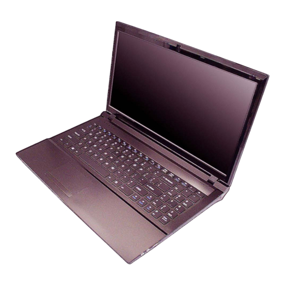
Introduction External Locator - Front View with LCD Panel Open Figure 1 Front View with LCD Pan- el Open 1. Built-In PC Camera (Optional) 2. LCD 3. Power Button 4. LED Status Indicators 5. Keyboard 6. Built-In Microphone 7. Touchpad & Buttons 1 - 4 External Locator - Front View with LCD Panel Open... -
Page 17: External Locator - Front And Rear View
Introduction External Locator - Front and Rear View Figure 2 Front View 1. LED Power Indicators Figure 3 Rear View 1. Security Lock Slot 2. Battery External Locator - Front and Rear View 1 - 5... -
Page 18: External Locator - Left & Right Side View
Introduction External Locator - Left & Right Side View Figure 4 Left Side View 1. DC-In Jack 2. External Monitor Port 3. RJ-45 LAN Jack 4. HDMI Port 5. 2 * USB 2.0 Ports 6. Vent 7. Multi-in-1 Card Reader Figure 5 Right Side View 1. -
Page 19: External Locator - Bottom View
Introduction External Locator - Bottom View Figure 6 Bottom View 1. Vent 2. Component Bay Cover 3. Hard Disk Bay Cover 4. Speakers 5. Battery 6. USIM Card Cover Overheating To prevent your com- puter from overheating make sure nothing blocks the vent/fan in- takes while the com-... -
Page 20: Mainboard Overview - Top (Key Parts)
Introduction Mainboard Overview - Top (Key Parts) Figure 7 Mainboard Top Key Parts 1. JMB261 2. Clock Generator 3. ITE 8502E 1 - 8 Mainboard Overview - Top (Key Parts) -
Page 21: Mainboard Overview - Bottom (Key Parts)
Introduction Mainboard Overview - Bottom (Key Parts) Figure 8 Mainboard Bottom Key Parts 1. Power IC 2. CPU Socket (no CPU installed) 3. Mini-Card Connector (Wireless Lan Module) 4. Memory Slots DDR3 SO-DIMM 5. Half Mini-Card Connector (3G Module) 6. Audio AMP 7. -
Page 22: Mainboard Overview - Top (Connectors)
Introduction Mainboard Overview - Top (Connectors) Figure 9 Mainboard Top Connectors 1. USB Ports 2. Speaker Cable Connector 3. Microphone Cable Connector 4. Click Board LED Connector 5. Touch Pad Cable Connector 6. Audio Cable Connector 7. Keyboard Cable Connector 8. -
Page 23: Mainboard Overview - Bottom (Connectors)
Introduction Mainboard Overview - Bottom (Connectors) Figure 10 Mainboard Bottom Connectors 1. Bluetooth Cable Connector 2. ODD Connector 3. HDD Connector 4. CMOS Battery Connector 5. Fan Cable Connector 6. RJ-45 LAN Jack 7. External Monitor Port 8. DC-In Jack 9. - Page 24 Introduction 1 - 12...
-
Page 25: Disassembly
Chapter 2: Disassembly Overview This chapter provides step-by-step instructions for disassembling the C5100Q/C5100Q-C/C5105/C5105-C series note- book’s parts and subsystems. When it comes to reassembly, reverse the procedures (unless otherwise indicated). We suggest you completely review any procedure before you take the computer apart. -
Page 26: Maintenance Tools
Disassembly NOTE: All disassembly procedures assume that the system is turned OFF, and disconnected from any power supply (the battery is removed too). Maintenance Tools The following tools are recommended when working on the notebook PC: • M3 Philips-head screwdriver •... -
Page 27: Maintenance Precautions
Disassembly Maintenance Precautions The following precautions are a reminder. To avoid personal injury or damage to the computer while performing a re- moval and/or replacement job, take the following precautions: Power Safety Warning 1. Don't drop it. Perform your repairs and/or upgrades on a stable surface. If the computer falls, the case and other Before you undertake components could be damaged. -
Page 28: Disassembly Steps
Disassembly Disassembly Steps The following table lists the disassembly steps, and on which page to find the related information. PLEASE PERFORM THE DISASSEMBLY STEPS IN THE ORDER INDICATED. To remove the Battery: To remove the Bluetooth Module: 1. Remove the battery page 2 - 5 1. -
Page 29: Removing The Battery
Disassembly Removing the Battery Figure 1 Battery Removal 1. Turn the computer off, and turn it over. 2. Slide the latch in the direction of the arrow. a. Slide latch at point 1 to- 3. Slide the latch in the direction of the arrow, and hold it in place. wards the unlock symbol 4. -
Page 30: Removing The Hard Disk Drive
Disassembly Removing the Hard Disk Drive The hard disk drive can be taken out to accommodate other 2.5" serial (SATA) hard disk drives with a height of 9.5mm Figure 2 (h). Follow your operating system’s installation instructions, and install all necessary drivers and utilities (as outlined in HDD Assembly Chapter 4 of the User’s Manual) when setting up a new hard disk. - Page 31 Disassembly 3. Remove the hard disk bay cover Figure 3 4. Grip the tab and slide the hard disk in the direction of arrow HDD Assembly 5. Lift the hard disk out of the bay Removal (cont’d.) 6. Remove screws and the mylar cover from the hard disk 7.
-
Page 32: Removing The Optical (Cd/Dvd) Device
Disassembly Removing the Optical (CD/DVD) Device Figure 4 Optical Device 1. Turn off the computer, remove the battery (page 2 - 5) and hard disk (page 2 - Removal 2. Remove the screw at point 3. Use a screwdriver to carefully push out the optical device at point a. -
Page 33: Removing The System Memory (Ram)
Disassembly Removing the System Memory (RAM) Figure 5 RAM Module The computer has two memory sockets for 200 pin Small Outline Dual In-line Memory Modules (SO-DIMM) supporting Removal DDRIII (DDR3) Up to 1066/1333 MHz. The main memory can be expanded up to 8GB. The SO-DIMM modules sup- ported are 1024MB and 2048MB DDRIII Modules. - Page 34 Disassembly 5. Pull the latches to release the second module if necessary. 6. Insert a new module holding it at about a 30° angle and fit the connectors firmly into the memory slot. 7. The module will only fit one way as defined by its pin alignment. Make sure the module is seated as far into the slot as it will go.
-
Page 35: Removing And Installing A Processor
Disassembly Removing and Installing a Processor Figure 6 Processor Removal Processor Removal Procedure 1. Turn off the computer, turn it over, and remove the battery (page 2 - 5) and the component bay cover (page 2 - a. Locate the heat sink. 2. - Page 36 Disassembly 5. Turn the release latch towards the unlock symbol to release the CPU (Figure 7d). Figure 7 6. Carefully (it may be hot) lift the CPU up and out of the socket (Figure 7e). Processor Removal 7. Reverse the process to install a new CPU. (cont’d) 8.
- Page 37 Disassembly Processor Installation Procedure Figure 8 1. Insert the CPU , pay careful attention to the pin alignment, it will fit only one way (DO NOT FORCE IT!), and turn Processor Installation the release latch towards the lock symbol (Figure 8b).
-
Page 38: Removing The 3G Module
Disassembly Removing the 3G Module Figure 9 3G Module Removal 1. Turn off the computer, turn it over, and remove the battery (page 2 - 5) and the component bay cover (page 2 - 2. The 3G module will be visible at point on the mainboard (Figure 9a). -
Page 39: Removing The Wireless Lan Module
Disassembly Removing the Wireless LAN Module Figure 10 Wireless LAN 1. Turn off the computer, turn it over, and remove the battery (page 2 - 5) and the component bay cover (page 2 - Module Removal 2. The Wireless LAN module will be visible at point on the mainboard (Figure 10a). -
Page 40: Removing The Bluetooth Module
Disassembly Removing the Bluetooth Module Figure 11 Bluetooth Module 1. Turn off the computer, turn it over, and remove the battery (page 2 - 5) and the component bay cover (page 2 - Removal 2. The Bluetooth module will be visible at point on the mainboard (Figure 11a). -
Page 41: Removing The Keyboard
Disassembly Removing the Keyboard Figure 12 Keyboard Removal 1. Turn off the computer, and remove the battery (page 2 - 2. Remove screws from the bottom of the computer. Press at point to unsnap the LED cover module (you a. Remove screws from the bottom of the computer. - Page 42 Disassembly 2 - 18...
-
Page 43: Part Lists
Part Lists Appendix A:Part Lists This appendix breaks down the C5100Q/C5100Q-C/C5105/C5105-C series notebook’s construction into a series of il- lustrations. The component part numbers are indicated in the tables opposite the drawings. Note: This section indicates the manufacturer’s part numbers. Your organization may use a different system, so be sure to cross-check any relevant documentation. -
Page 44: Part List Illustration Location
Part List Illustration C5100Q/C5100Q-C/C5105/ Part Location C5105-C page A - 3 Top (C5105Q) page A - 4 Top (C5100Q) Bottom page A - 5 page A - 6 DVD Dual Drive page A - 7 A - 2 Part List Illustration Location... -
Page 45: Top (C5105Q
Part Lists Top (C5105Q) Figure A - 1 Top (C5105Q) 非 耐 落 灰 色 Top (C5105Q) A - 3... -
Page 46: Top (C5100Q
Part Lists Top (C5100Q) Figure A - 2 Top (C5100Q) 非耐落 灰色 A - 4 Top (C5100Q) -
Page 47: Bottom
Part Lists Bottom Figure A - 3 Bottom Bottom A - 5... -
Page 48: Dvd Dual Drive
Part Lists DVD Dual Drive Figure A - 4 DVD Dual Drive 非 耐 落 志 精 A - 6 DVD Dual Drive... -
Page 49: Lcd
Part Lists Figure A - 5 頭厚 非耐落 LCD A - 7... - Page 50 Part Lists A - 8...
- Page 51 Schematic Diagrams Appendix B:Schematic Diagrams This appendix has circuit diagrams of the C5100Q/C5100Q-C/C5105/C5105-C notebook’s PCB’s. The following table indicates where to find the appropriate schematic diagram. Diagram - Page Diagram - Page Diagram - Page Table B - 1 Schematic...
-
Page 52: Schematic Diagrams
Schematic Diagrams System Block Diagram CLEVO C5100Q System Block Diagram SYSTEM POWER +VCORE AC-IN,CHARGER VDD3,VDD5,3.3V,5V CLOCK GEN. Intel Penryn Memory Termination SLG8SP513V PROCESSOR 1.8V,1.05VS 478pins uFCBGA DDRIII SO-DIMM1 14.318 MHz 1.5V,0.75VS DDRIII SO-DIMM2 Audio Board MIC IN,HEADPHONE 0.5"~5.5" USB11 667/800 MHz... -
Page 53: Clock Generator
Schematic Diagrams Clock Generator CLOCK GENERATOR 3 . 3 V S _ G 1. 0 5 V S _ G 1 . 0 5 V S R 1 79 *2 0m i l _ sh o rt _ 04 C 50 4 C 2 47 C 2 1 8 C 50 3... -
Page 54: Penryn (Socket-P)1/2
Schematic Diagrams Penryn (Socket-P)1/2 J S K T1 A H _A # [ 35 : 3 ] H_A # 3 A [ 3] # A DS # H _A D S# H_A # 4 J S KT 1 B A [ 4] # B N R # H _B N R# H_A # 5... -
Page 55: Penryn (Socket-P)2/2
Schematic Diagrams Penryn (Socket-P)2/2 V C OR E PLACE NEAR CPU C 4 1 7 C 4 1 9 C 4 2 3 C 4 1 8 C 1 7 C 2 3 C2 7 C 3 1 JS K T1 D V S S [ 0 01 ] V S S [0 8 2] P 2 1... -
Page 56: Cantiga 1/7, Host
Schematic Diagrams CANTIGA 1/7, HOST U 1 5A H _A# [ 35 :3 ] 3 A1 4 H_ A# 3 H _ D# [6 3 :0 ] H_ A# _3 H_ D# 0 C 15 H_ A# 4 H _D #_ 0 H_ A# _4 H_ D# 1 F1 6... -
Page 57: Cantiga 2/7, Graphics
Schematic Diagrams CANTIGA 2/7, Graphics 1.05 V M _ P EG 3.3 V S L1 2 U15C PEG_C OMPI and t he PE G_COM PO pi ns sh ould be *20mil _ shor t_04 R120 short ed at the packa ge an d the n rou ted t o one R113 R11 2 R 114... -
Page 58: Cantiga 3/7
Schematic Diagrams CANTIGA 3/7 U 1 5 B A P 2 4 S A _ C K _ 0 M_ C LK _A _D D R 0 1 2 A T 2 1 1 . 5 V D MI X2 s el ec t L ow = DM I x 2 R 95 S A _ C K _ 1... -
Page 59: Cantiga 4/7
Schematic Diagrams CANTIGA 4/7 Z o= 5 5O? 5% Z o= 5 5O? 5 % U 1 5E M _B _D Q[ 63 :0 ] M_ B_ DQ 0 A K4 7 B C1 6 U1 5 D M _A _D Q[6 3 :0 ] S B _ D Q_ 0 S B _ BS _0 M_ B _ B S 0 # 1 3... -
Page 60: Cantiga 5/7
Schematic Diagrams CANTIGA 5/7 U 1 5 G 1 . 5 V 1. 05 V S U 1 5 F 1 . 05 V S 8.7A A P 3 3 W 2 8 V C C _ S M _ 1 V C C _ A X G_ N C T F _1 A N 3 3 V 2 8... -
Page 61: Cantiga 6/7
Schematic Diagrams CANTIGA 6/7 1 0m ils C 4 8 4 C 47 6 C 4 73 1 . 0 5 V S 4 . 7 u _6 . 3 V _ X 5 R _ 0 6 0 . 0 1 u _1 6 V _ X 7 R _ 0 4 0 . -
Page 62: Cantiga 7/7
Schematic Diagrams CANTIGA 7/7 U 1 5 I U 1 5 J AU 4 8 A M3 6 B G 21 AH 8 V SS_ 1 VS S_ 1 0 0 V SS _ 19 9 V SS_ 2 9 7 AR 4 8 A E3 6 L 12... -
Page 63: Ddriii So-Dimm A
Schematic Diagrams DDRIII SO-DIMM A SO-DIMM A J _ D I M M1 A M_ A _ A [ 1 4 : 0 ] M _ A _D Q[ 6 3 : 0 ] 8 M _A _A 0 M_ A _ D Q 0 D Q 0 M _A _A 1 M_ A _ D Q 1... -
Page 64: Ddriii So-Dimm B
Schematic Diagrams DDRIII SO-DIMM B SO-DIMM B J _D I MM 2 A M _ B _ A [ 1 4: 0 ] M_ B _ D Q [ 6 3 : 0] M _ B _A 0 M _ B _D Q0 D Q0 M _ B _A 1 M _ B _D Q1... -
Page 65: Panel, Crt
Schematic Diagrams Panel, CRT 3. 3 V S 5 V S R N 2 7 2. 2 K _ 8 P 4 R _ 04 U 1 3 C R T_ D D C A C L K D A C _ D D C A C LK D D C _ I N 1 D D C _ OU T 1 C R T_ D D C A D A T... -
Page 66: Inverter, Bluetooth, Fan
Schematic Diagrams Inverter, Bluetooth, Fan INVERTER CONNECTOR 3 . 3 V 3 . 3 V R 4 6 *1 0 0K _0 4 U 3 A 3. 3 V 7 4L V C 0 8P W C 44 B K L_ E N U 3B 7 4 LV C 0 8P W * . -
Page 67: Ich9M 1/4, Sata
Schematic Diagrams ICH9M 1/4, SATA R TC V C C 20m ils C 2 7 3 1 5 p _5 0 V _ N P O _ 04 20m ils C 2 28 R 18 6 R 4 0 6 1 TJ S 1 2 5 D J 4 A 4 20 P _ 3 2 . -
Page 68: Ich9M 2/4, Pci, Usb
Schematic Diagrams ICH9M 2/4, PCI, USB U 17 D N 2 9 V 27 P C I E _ R X N 1 _W LA N P E R N 1 D MI 0R X N D M I _ R X N 0 7 N 2 8 V 26 P C I E _ R X P 1 _ W L A N... -
Page 69: Ich9M 3/4
Schematic Diagrams ICH9M 3/4 3 . 3 V S B _ G P I O2 1 2 , 1 2 , 1 3 I C H _S M B C LK 0 R 2 1 2 10 K _ 0 4 P C I E _W A K E # S B _ G P I O1 9 DDR3, CLK GEN... -
Page 70: Ich9M 4/4
Schematic Diagrams ICH9M 4/4 R T C V C C U 17 F U 1 7 E 20mil s 1.7A A 2 3 A 15 A A 26 1. 0 5 V S Layou t note: V C C R TC V C C 1 _0 5 [ 1 ] V S S [ 1 ] V S S [ 1 0 7 ]... -
Page 71: Hdmi
Schematic Diagrams HDMI HDMI HDMI CONNECTOR Saf ty Requ ire 5V S J_H DMI1 R401 1_04 R 323 1_04 C 427 C42 6 *22u_6.3V _Y5V _08 H DMI_D0N R438 0_04 HDM I_DAT A0N H DMI_HP D 22u_6.3V _X 5R_08 HO T PLU G DE TEC T H DMI_D0P HDM I_DAT A0P R439... -
Page 72: Kbc-Ite It8502E
Schematic Diagrams KBC-ITE IT8502E K B C _ A V D D L2 1 H C B 10 0 5 K F -1 21 T 2 0 VOL TA GE MO DEL _I D V D D 3 V D D 3 V D D 3 C 3 3 9 C 28 9... -
Page 73: Card Reader/Lan Jmb261C
Schematic Diagrams Card Reader/LAN JMB261C S D _ C L K JMC261 C Sw it ch ing R eg ul at or 3. 3 V _ L A N ne ar P in#4 1 C 64 3 cl os e to PI N3 3 D V D D * 10 p _ 50 V _ N P O_ 0 4 R 4 1 2... -
Page 74: Audio Codec Vt1812
Schematic Diagrams Audio Codec VT1812 CODEC ( VT1812 ) 3.3V S 1.5VS R289 R28 7 *S CS 551V -30 PIN 25 ,PI N38 ? 1 ? 10 uF/ .1u F *0_0 4 *2 8m il_sho r t_0 6 5VS _A UD *28m i l _short_06 5V S C 379... -
Page 75: Audio Amp
Schematic Diagrams Audio AMP AMP (TPA6017 or N7010) 5VS _REAR L 47 *R0805 _short C571 C559 C551 C5 63 0. 1u_16V_Y5V _ 04 10 u_10V_Y5V _0 8 *10u _10V _ Y5V _08 *10u_6. 3V _X5R_06 F RONT-L LI N- R465 0_04 C577 1u _6.3V_X 5R_04... -
Page 76: Hdd, Odd, Mdc, Tp, Conn, 3G
Schematic Diagrams HDD, ODD, MDC, TP, Conn, 3G Close to J _ OD D 1 connector S A T A T X P 1 _ R C 4 8 9 0 . 0 1 u _1 6 V _ X7 R _0 4 C 28 0 S A T A TX P 1 1 6 S A T A T X N 1 _ R... -
Page 77: New Card, Usb, Mini Pcie
Schematic Diagrams New Card, USB, Mini PCIE 3 . 3V S N ew C ard For C 4100 Q NEW CARD C 3 7 8 *. 1U _1 0 V _ X7 R _0 4 L P C _R S T # 3 . -
Page 78: Led, Ccd, Audio Conn
Schematic Diagrams LED, CCD, Audio Conn V D D 3 V D D 3 5 V S 3 . 3 V S 3 . 3 V S C 6 4 0 * 0. 1u _ 10 V _ X 7R _ 04 R 29 7 R 2 9 8 V D D 3... -
Page 79: System Power, Pwr Sw
Schematic Diagrams System Power, PWR SW 5V,3.3V,5VS,3.3VS,1.5VS P Q 41 S Y S 15 V 1. 5 V P Q 5 3 P Q 44 ME 44 1 0 A D -G 1 . 5 V S M E 4 41 0 A D -G M E 44 1 0 A D -G S Y S 1 5 V V D D 5... -
Page 80: Ac_In, Charger
Schematic Diagrams AC_In, Charger P Q 27 charg e Cu rrent 3.2 A V I N P 2 0 03 E V G Charg e Vo ltage 12. 6V J _ A C -J A C K 1 Total Power 60W 5 0 93 2 -0 03 0 1 -00 1 P L 4 P Q2 2... -
Page 81: Vcore
Schematic Diagrams VCORE VCORE FOR PENRYN CPU V I N V I N V -R C 1 P C 1 0 P C 8 0 P C 81 P C 1 2 P D 1 1 u _ 1 0V _0 6 1 0 00 p _ 5 0 V _ X7 R _ 0 4 R B 0 5 4 0 S 2 P R 7 9... -
Page 82: Vdd3, Vdd5
Schematic Diagrams VDD3, VDD5 V R E F P R 1 2 5 *0 _ 04 P R 1 2 8 0 _ 04 P C 1 4 4 1 u _ 10 V _ 0 6 P R 1 2 3 P R 12 9 E N _ 3 V E N _ 5 V... -
Page 83: 1.8V/1.05Vs
Schematic Diagrams 1.8V/1.05VS P R 1 0 9 * 1 5 m i l _ s h o rt Vout=0.75V(1+Ra/Rb) V I N P D 9 P C 2 3 P C 2 7 P C 2 4 R B 0 5 4 0S 2 0 . -
Page 84: 1.5V,0.75Vs
Schematic Diagrams 1.5V,0.75VS 3.3 V P R5 3 P R5 5 P R52 P D4 10 0K _ 04 1 M_0 4 1 0_ 06 V 1. 5 RB 0 54 0S 2 P U1 P R5 6 10 _0 6 V DDQ S P GD 1 .5V _ P WRG D 18... -
Page 85: Click Board
Schematic Diagrams Click Board CLICK BOARD CV DD3 CVD D3 C VDD3 CV DD3 CR 360 CR359 CR 361 CR358 220_04 220_04 220_04 0.1u_16V_Y5V _04 *0.1u_16V _Y5V_04 *0.1u_16V_Y5V _04 220_04 POW ER O N C5VS C5VS CV DD3 BAT LED CD 27 CD26 CGND... -
Page 86: Audio Board/Usb
Schematic Diagrams Audio Board/USB USB PORT A _U S B V C C A L 5 A _ U S B V C C2 H C B 1 6 0 8K F -12 1 T 25 60 mil A _ U S B V C C A _U S B V C C A U 1 A C 1... -
Page 87: Power Switch & Lid Board
Schematic Diagrams Power Switch & Lid Board POWER SW & LED & HOT KEY S _ 3 .3V S S _3 .3 V POWER LID SWITCH IC SWITCH S D2 S _ 3 . 3V S S _ 3 .3 V S R2 *B A V 99 R E CT IF I E R S _ 3 . -
Page 88: B - 38 External Odd Board
Schematic Diagrams External Odd Board ODD BOARD FOR E5120Q QJ _ OD D 2 Q J_ O DD 1 QJ _S ATA_ TX P1 QJ _S ATA_ TX N 1 QJ _S ATA_ R X N 1 QJ _S ATA_ R X P1 Q GN D Q GND Sheet 37 of 38... -
Page 89: Power Sequence V1.0
Schematic Diagrams Power Sequence V1.0 C5100 V1.0 POWER ON SEQUENCE PWR_SW# DD_ON 2.06 ms 3.3V 2.2 3ms 2.8 ms 1.5V 1.8V 76 .2ms RSMRST# 1 29.6 6ms Sheet 38 of 38 PWR_BTN# 8 2.9m s Power Sequence 9 7.46 ms SUSC# V1.0 4 .94m s... - Page 90 Schematic Diagrams B - 40...
-
Page 91: Updating The Flash Rom Bios
Download the BIOS computer model. 1. Go to www.clevo.com.tw and point to E-Services and click E-Channel. Note that BIOS versions 2. Use your user ID and password to access the appropriate download area (BIOS), and download the latest BIOS files... -
Page 92: Use The Flash Tools To Update The Bios
BIOS Update Use the flash tools to update the BIOS 1. Make sure you are not loading any memory management programs such as HIMEM by holding the F8 key as you see the message “Starting MS-DOS”. You will then be prompted to give “Y” or “N” responses to the programs being loaded by DOS. - Page 93 www.s-manuals.com...
Need help?
Do you have a question about the C5100Q and is the answer not in the manual?
Questions and answers