Table of Contents

Related Manuals for Panasonic TH-C42FD18


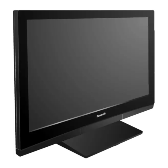
Summary of Contents for Panasonic TH-C42FD18
- Page 1 ORDER NO. MTNC080533CE B34 Canada: B07 42 inch Class 1080p Plasma HDTV TH-C42FD18 Model No. GPF11DU Chassis © 2008 Matsushita Electric Industrial Co., Ltd. All rights reserved. Unauthorized copying and distribu- tion is a violation of law.
-
Page 2: Safety Precautions
1 Safety Precautions 1.1. General Guidelines 1. When conducting repairs and servicing, do not attempt to modify the equipment, its parts or its materials. 2. When wiring units (with cables, flexible cables or lead wires) are supplied as repair parts and only one wire or some of the wires have been broken or disconnected, do not attempt to repair or re-wire the units. -
Page 3: Prevention Of Electrostatic Discharge (Esd) To Electrostatically Sensitive (Es) Devices
2 Warning 2.1. Prevention of Electrostatic Discharge (ESD) to Electrostatically Sensitive (ES) Devices Some semiconductor (solid state) devices can be damaged easily by static electricity. Such components commonly are called Elec- trostatically Sensitive (ES) Devices. Examples of typical ES devices are integrated circuits and some field-effect transistors and semiconductor [chip] components. -
Page 4: About Lead Free Solder (Pbf)
2.2. About lead free solder (PbF) Note: Lead is listed as (Pb) in the periodic table of elements. In the information below, Pb will refer to Lead solder, and PbF will refer to Lead Free Solder. The Lead Free Solder used in our manufacturing process and discussed below is (Sn+Ag+Cu). That is Tin (Sn), Silver (Ag) and Copper (Cu) although other types are available. -
Page 5: Service Navigation
3 Service Navigation 3.1. Service Hint Board Name Function Board Name Function Power Supply Data Driver (Lower Right) DC-DC Converter Data Driver (Lower Left) Speaker out, Sound Processor Scan Drive AV Terminal, AV Switch Scan out (Upper) Digital Signal Processor, Micon, HDMI Interface Scan out (Lower) Peaks Lite 2p Sustain Drive... -
Page 6: Applicable Signals
3.2. Applicable signals * Mark: Applicable input signal for Component (Y, PB, PR), HDMI and PC horizontal frequency (kHz) vertical frequency (Hz) COMPONENT HDMI 525 (480) / 60i 15.73 59.94 525 (480) /60p 31.47 59.94 750 (720) /60p 45.00 59.94 1,125 (1,080) /60i 33.75 59.94... -
Page 7: Specifications
4 Specifications Power Source AC 120 V, 60 Hz Power Consumption Maximum 573 W Standby condition 0.2 W Plasma Display panel Drive method AC type Aspect Ratio 16:9 Visible screen size 42 inch class (41.6 inches measured diagonally) (W × H × Diagonal) 36.2 inch ×... -
Page 8: How To Enter Into Service Mode
5 Service Mode 5.1. How to enter into Service Mode While pressing [VOLUME ( - )] button of the main unit, press [INFO] button of the remote control three times within 2 seconds. 5.1.1. Key command [1] button...Main items Selection in forward direction [2] button...Main items Selection in reverse direction [3] button...Sub items Selection in forward direction [4] button...Sub items Selection in reverse direction... -
Page 9: Contents Of Adjustment Mode
Contents of adjustment mode 5.1.2. • Value is shown as a hexadecimal number. • Preset value differs depending on models. • After entering the adjustment mode, take note of the value in each item before starting adjustment. Main item Sub item Sample Data Remark ADJUST... -
Page 10: Service Tool Mode
5.2. Service tool mode 5.2.1. How to access 1. Select [SRV-TOOL] in Service Mode. 2. Press [OK] button on the remote control. 5.2.2. Display of SOS History SOS History (Number of LED blinking) indication. From left side; Last SOS, before Last, three occurrence before, 2nd occurrence after shipment, 1st occurrence after shipment. This indication except 2nd and 1st occurrence after shipment will be cleared by [Self-check indication and forced to factory ship- ment setting]. -
Page 11: Hotel Mode
5.3. Hotel mode 1. Purpose Restrict a function for hotels. item Function 2. Access command to the Hotel mode setup menu Mode Select hotel mode ON/OFF In order to display the Hotel mode setup menu, please Input Select input signal modes. enter the following command (within 2 second). -
Page 12: Troubleshooting Guide
6 Troubleshooting Guide Use the self-check function to test the unit. 1. Checking the IIC bus lines 2. Power LED Blinking timing 6.1. Check of the IIC bus lines 6.1.1. How to access Self-check indication only: Produce TV reception screen, and while pressing [VOLUME ( - )] button on the main unit, press [OK] button on the remote control for more than 3 seconds. -
Page 13: Power Led Blinking Timing Chart
6.2. Power LED Blinking timing chart 1. Subject Information of LED Flashing timing chart. 2. Contents When an abnormality has occurred the unit, the protection circuit operates and reset to the stand by mode. At this time, the defective block can be identified by the number of blinks of the Power LED on the front panel of the unit. - Page 14 6.3. No Power First check point There are following 2 states of No Power indication by power LED. 1. No lit 2. Red is lit then turns red blinking a few seconds later. (See 6.2.)
- Page 15 6.4. No Picture...
-
Page 16: Local Screen Failure
6.5. Local screen failure Plasma display may have local area failure on the screen. Fig-1 is the possible defect P.C.B. for each local area. Fig-1... -
Page 17: Disassembly And Assembly Instructions
7 Disassembly and Assembly Instructions 7.1. Remove the Rear cover 5. Remove the PB-Board. 1. See Service Hint (Section 3) 7.2. Remove the Fan unit 1. Unlock the cable clampers to free the cable. 2. Remove the screws (×3 3. Remove the relay connectors and remove the Fan unit. 7.4. -
Page 18: Remove The A-Board Unit
7.5. Remove Rear Terminal cover , ×2 1. Remove the screws (×4 2. Remove the Rear Terminal cover. 7. Remove the screws (×7 8. Remove the molding props (×13 9. Remove the P-Board. 7.6. Remove the A-Board unit 1. Unlock the cable clampers to free the cable. 2. -
Page 19: Remove The Su-Board
7.8. Remove the SU-Board 7.10. Remove the SC-Board 1. Remove the flexible cables (SU1, SU2, SU3 and SU4) 1. Remove the SU-Board and SD-Board. (See section 7.8. connected to the SU-Board. and 7.9.) 2. Remove the flexible cable (SU11-SD11) and the bridge 2. -
Page 20: Remove The Stand Brackets
7.12. Remove the Stand brackets 7.14. Remove the C1-Board 1. Remove the Plasma panel section from the servicing 1. Remove the A-Board unit. (See section 7.6.) stand and lay on a fiat surface such as a table (covered) 2. Remove the Stand bracket L. (See section 7.12.) with the Plasma panel surface facing downward. -
Page 21: Remove The C2-Board
7.15. Remove the C2-Board 7.16. Remove the Front bracket 1. Remove the A-Board unit. (See section 7.6.) 1. Unlock the cable clampers to free the cable. 2. Remove the stand bracket R. (See section 7.12.) 2. Disconnect the connectors (A11, A51 and A52). (See sec- tion 7.6.) 3. -
Page 22: Remove The Speakers
11. Disconnect the connector (G51) and remove the G- 2. Remove the cabinet assy and the plasma panel fastening Board. , ×6 screws (×4 7.18. Remove the Speakers 1. Disconnect the relay connectors 2. Remove the screws (×4 each) and remove the Speaker (L, R). -
Page 23: Remove The S-Board
7.22. Remove the plasma panel (fin- ished) 1. Place the new plasma panel (finished) on the flat surface of the table (covered by a soft cloth), with the plasma panel surface facing downward. 2. Attach the C1-Board and the C2-Board, connect the flexi- ble cables (×15) from the plasma panel to the C1-Board and the C2-Board, and fit the flexible cable holders. -
Page 24: Measurements And Adjustments
8 Measurements and Adjustments 8.1. Adjustment Procedure 8.1.1.2. Adjustments Adjust driver section voltages referring the panel data on the 8.1.1. Driver Set-up panel data label. Check or adjust the following voltages with the multimeter. 8.1.1.1. Item / Preparation 1. Input a white signal to plasma video input. Name Test Point Voltage... -
Page 25: Initialization Pulse Adjust
8.1.2. Initialization Pulse Adjust 1. Input the White signal to plasma video input. 2. Set the picture controls as follows. Picture menu : Vivid Normal : Set Aspect : Full 3. Connect Oscilloscope to TPSC1 (SC). Check the voltage (T2) at 100 us period on the down slop. Test point Volume Level... - Page 26 8.1.4. Adjustment Volume Location 8.1.5. Test Point Location...
-
Page 27: White Balance Adjustment
8.2. Adjustment 8.2.1. White balance adjustment Name of measuring instrument Connection Remarks • W/B pattern Component input • Color analyzer Panel surface (Minolta CA-100 or equivalent) Procedure Remarks • Ensure aging is adequate. • Make sure the front panel to be used on the final set is fitted. •... -
Page 29: Block Diagram
FAN_A-D +5V(STB) FAN CONT FAN POWER +5V(S) +30V(BT) BT+30V PB30 +9/7.2V +9V(S) PB31 DIGITAL SIGNAL PROCESSOR FAN SOS FAN SOS DET +5V(STB) STB+3.3V +3.3V(STB) PB32 CIRCUIT PB36 (LED:11TIMES) (LED:11TIMES) PB37 FAN CONTROL TH-C42FD18 TH-C42FD18 Block (1/6) Diagram Block (1/6) Diagram... - Page 30 VIDEO DATA DATA DATA DATA DATA DATA DATA DATA DATA DATA DATA DATA DATA DATA DATA DATA DRIVER DRIVER DRIVER DRIVER DRIVER DRIVER DRIVER DRIVER DRIVER DRIVER DRIVER DRIVER DRIVER DRIVER DRIVER TH-C42FD18 TH-C42FD18 Block (2/6) Diagram Block (2/6) Diagram...
- Page 31 DDR I/F DDR2 #0/#1 SD DATA IC8004 CLOCK CLOCK GEN IIC0 SD CARD SD DATA IC8502 IIC1 RESET NOR FLASH IIC2 SBI2 CPU BUS I/F SBO2 IIC_IF EEPROM IC8001 IIC3 IC8503 Peaks Lite2p TH-C42FD18 TH-C42FD18 Block (3/6) Diagram Block (3/6) Diagram...
- Page 32 FAN SOS +9/7.2V D851 FAN SOS SW2500 PB31 D852 FAN CONT (LED:11TIMES) (LED:11TIMES) POWER FAN CONT PB32 D856 SWITCH D857 D861 PB36 +15V(FAN) PB37 IC850 D860 +9/7.2V FAN(80MM)A-D POWER SWITCH TH-C42FD18 FAN CONTROL TH-C42FD18 Block (4/6) Diagram Block (4/6) Diagram...
- Page 33 ERROR DET (LED:6TIMES) (LED:6TIMES) SOS6_SC1 SOS6_SC1 IIC_DATA2 RESET RESET (LED:7TIMES) (LED:7TIMES) SOS7_SC2 SOS7_SC2 COLD IIC2 IIC_CLK2 +15V(P) PANEL SOS PANEL SOS +15V(P) AC INLET PANEL STATUS PANEL STATUS AC100V +15V(P) AC CORD 50/60Hz TH-C42FD18 TH-C42FD18 Block (5/6) Diagram Block (5/6) Diagram...
- Page 34 C2 DATA DRIVER (LEFT) +5V(P)DET SS33 CONTROL DATA SOS8_SS IC17201,03 IC17101 IC17103 VIDEO DATA BUFFER BUFFER SUSTAIN CONTROL BUFFER BUFFER BUFFER BUFFER IC17204 +5V(P) IC17102 IC17202 SS35 PANEL DRIVER PLASMA PANEL PANEL DRIVER TH-C42FD18 TH-C42FD18 Block (6/6) Diagram Block (6/6) Diagram...
-
Page 35: Wiring Connection Diagram
10 Wiring Connection Diagram 10.1. Caution statement. Caution: Please confirm that all flexible cables are assembled correctly. Also make sure that they are locked in the connectors. Verify by giving the flexible cables a very slight pull. 10.2. Wiring (1) - Page 36 10.3. Wiring (2)
- Page 37 10.4. Wiring (3)
- Page 38 10.5. Wiring (4)
- Page 39 10.6. Wiring (5)
-
Page 41: Schematic Diagram
11 Schematic Diagram 11.1. Schematic Diagram Note... -
Page 42: P-Board (1/2) Schematic Diagram
11.2. P-Board (1/2) Schematic Diagram AC CORD RECTIFIER <Exchange board only> <Exchange board only> PFC CONTROL <Exchange board only> P-BOARD ETX2MM702MFH (1/2) TH-C42FD18 TH-C42FD18 P-Board (1/2) Schematic Diagram P-Board (1/2) Schematic Diagram... -
Page 43: P-Board (2/2) Schematic Diagram
<Exchange board only> POWER CONTROL <Exchange board only> COLD COLD Vsus POWER SUPPLY <Exchange board only> CONTROL SWITCH +15V ERROR DET <Exchange board only> COLD COLD +5V(P) <Exchange board only> TH-C42FD18 TH-C42FD18 P-Board (2/2) Schematic Diagram P-Board (2/2) Schematic Diagram... -
Page 44: Pb-Board Schematic Diagram
TP850 C861 0.1u C869 TP852 470u D859 R859 R871 B0JCME000037 C862 C860 L852 R872 0.1u 470u G0C101KA0167 TP851 D860 MAZ81100ML R874 R861 4.7k TP853 C859 D862 MAZ80330LL 0.1u R867 PB30 A-BOARD (A30) TH-C42FD18 TH-C42FD18 PB-Board Schematic Diagram PB-Board Schematic Diagram... - Page 45 AV3_S_DET 0.1u R7701 SDDAT1 GS52 KEY1 A-BOARD R7702 (A52) R7794 R7796 D.SW R7710 R7799 R7797 R7708 R7793 R7798 W.P . R7795 R7792 A-BOARD (A51) TH-C42FD18 TH-C42FD18 G, GS, K, and S-Board Schematic Diagram G, GS, K, and S-Board Schematic Diagram...
-
Page 46: Gh-Board Schematic Diagram
CLKG FL3805 0.01u J0MAB0000170 CLK+ HDMI_5V_DET3 GH10 K1FY121E0001 DDC5V HDMI IN 3 IC3801 R3811 C1AB00002835 4.7k HDMI EQUALIZER C3816 C3812 HDMI_CE1 0.01u 0.1u R3834 49.9 A-BOARD ZA3802 K4AD01D00005 (A11) GH11 ZA3801 K4AD01D00005 TH-C42FD18 TH-C42FD18 GH-Board Schematic Diagram GH-Board Schematic Diagram... - Page 47 VDD33 IC8001 IC8001 J0JHC0000045 0.1u IC8001 AF20 VDDIO IC8001 LVVDD12 IC8001 AC10 VDD33 IC8001 IC8001 AF21 C8080 IC8001 AF26 VDDIO C8076 C8075 IC8001 AC11 VDD33 IC8001 IC8001 AF24 0.1u 0.1u TH-C42FD18 TH-C42FD18 A-Board (1/12) Schematic Diagram A-Board (1/12) Schematic Diagram...
- Page 48 IC8003 MMDQ28 AB16 IC8001 CH0DQ16 VJUMP1005-S CH0DQ29 IC8003 R8020 MMDQ29 AA16 IC8001 CH0DQ23 R8021 VJUMP1005-S CH0DQ30 IC8003 MMDQ30 AD16 IC8001 CH0DQ20 R8022 VJUMP1005-S CH0DQ31 IC8003 MMDQ31 AF16 IC8001 CH0DQ19 IC8003 TH-C42FD18 TH-C42FD18 A-Board (2/12) Schematic Diagram A-Board (2/12) Schematic Diagram...
- Page 49 TP8519 NOR FLASH to other devices TVRP753S C4780 0.1u TP8518 SUB3.3V GS-BOARD R8512 R8533 (GS52) TP8546 TP8548 R8528 TRST TP8544 R8529 TRST R8530 to (1/12) TP8547 R8532 R5058 R5069 R5137 TH-C42FD18 TH-C42FD18 A-Board (3/12) Schematic Diagram A-Board (3/12) Schematic Diagram...
- Page 50 +INC PGND AG_KEY3 R5605 R5612 12.7k -INC PEAKS-LITE2 RESET IC3017 SUB3.3V C0EBM0000026 RESET IC F15V R5747 R5748 C5767 R5762 0.01u XRST to (1/12) AG_DTV_XRST C5766 to (3/12)(7/12) 0.01u C5765 0.047u TH-C42FD18 TH-C42FD18 A-Board (4/12) Schematic Diagram A-Board (4/12) Schematic Diagram...
- Page 51 DTV_V R3077 R3068 C3057 MAIN_R RF_V R3316 L3309 R3307 J0JCC0000269 PC_G_IN MAIN_L 4.7k R3078 R3301 R3303 R3313 AAM_R AAM_L R3302 R3305 C3061 C3023 R3311 PC_R_IN R3310 PC_V_IN PC_H_IN RF_L RF_R TH-C42FD18 TH-C42FD18 A-Board (5/12) Schematic Diagram A-Board (5/12) Schematic Diagram...
- Page 52 K7AAAY000003 TUNER_SUB_ON DVDD1.8V AG_TV_SUB_ON J0HAAB000036 to (7/12) TP3528 OPTICAL G-BOARD ECO_ON AG_ECO_ON (G51) AUDIO ALL_OFF C3157 VIH > 2.2V => PowerDown AC_GOOD/KEY VIL < 0.8V => active 0.1u >> RESETB TH-C42FD18 TH-C42FD18 A-Board (6/12) Schematic Diagram A-Board (6/12) Schematic Diagram...
- Page 53 AG_ECO_ON C1112 To D pri 0.1u to (12/12) AG_PANEL_READY AG_PANEL_READY AG_PANEL_ARARM AG_PANEL_ARARM Power Supply AG_ODU_DET/KEY3 to (4/12) AG_ODU_DET/KEY3 AG_KEY1(CON-PANE) to (6/12) AG_KEY1(CON-PANE) AG_R_LED_ON AG_R_LED_ON to (6/12) AG_RMIN to (6/12) AG_RMIN TH-C42FD18 TH-C42FD18 A-Board (7/12) Schematic Diagram A-Board (7/12) Schematic Diagram...
- Page 54 VOP11 C4224 LOSD13 VOP11 VOP20 6.3V RE_O- LOSD10 VOP20 VOP21 LOSD11 VOP21 RE_O+ C4213 C4214 C4215 ADIN 0.1u 0.1u 0.1u OSDYS ADIN R4294 EXB28V470JX GenX5 to (7/12) AG_BACK_VOUTENB AG_BACK_VOUTENB R4309 TH-C42FD18 TH-C42FD18 A-Board (8/12) Schematic Diagram A-Board (8/12) Schematic Diagram...
- Page 55 L4500 D4513 J0JHC0000078 Q4530 MAZ30560ML SUB3.3V SUB5V 2SB0709A0L L4502 N.C. JK4500 J0JHC0000078 RXB_CN K1FY119D0003 CLK- RXB_CP CLKG HDMI2 R4568 Q4531 CLK+ RXB_0N 2SB0709A0L GH-BOARD RXB_0P (GH11) RXB_1N RXB_1P RXB_2N RXB_2P TH-C42FD18 TH-C42FD18 A-Board (9/12) Schematic Diagram A-Board (9/12) Schematic Diagram...
- Page 56 SPDIF HDMI_LRCK AG_HPD3 DDCA_SCL EXB28V330JX HDMI_BCLK to (5/12) HDMI_BCLK AG_HDMI_REP_EN DDCA_SDA HDMI_SPDIF AG_HDMI_REP_EN C4614 0.1u HDMI_SPDIF C4613 C4634 C4612 0.01u AG_HDMI_5V_DET1 AG_HDMI_5V_DET1 AG_HDMI_5V_DET2 AG_HDMI_5V_DET2 AG_HDMI_CEC AG_HDMI_CEC AG_HDMI_MUX_SEL AG_HDMI_MUX_EN AG_HPD4 AG_HDMI_5V_DET4 TH-C42FD18 TH-C42FD18 A-Board (10/12) Schematic Diagram A-Board (10/12) Schematic Diagram...
- Page 57 C8376 C8337 0.01u 0.1u 0.01u 0.1u 0.1u C8338 0.1u C8339 C8340 SUB5V BT30V 0.1u 0.1u C8374 C8377 C8378 C8379 C8370 C8371 C8380 0.1u 0.01u 0.1u 1000p 0.01u 0.1u C8346 0.01u TH-C42FD18 TH-C42FD18 A-Board (11/12) Schematic Diagram A-Board (11/12) Schematic Diagram...
- Page 58 C4744 C4745 C4746 C4771 C4772 C4773 C4774 C4775 C4776 C4777 C4778 C4779 0.1u 1000p 1000p 1000p 0.1u 1000p 0.1u 0.1u 1000p 1000p 0.1u 1000p 0.1u 0.1u 1000p 0.1u 0.1u 0.1u TH-C42FD18 TH-C42FD18 A-Board (12/12) Schematic Diagram A-Board (12/12) Schematic Diagram...
- Page 59 D9808 SC_DRV_RST FP_CQR5 B0JCCE000008 FP_SC3 R9869 +15V Q9806 2SD0601A0L P15V_MOTO D9807 +15V PA9900 B0JCCE000008 R9870 K5H5022A0031 +15V C9859 C9858 0.01u R9197 SC_CQR4 CQR4 C9168 R9120 SC_CQR5 EXB2HV103JV 0.1u CQR5 R9202 TH-C42FD18 TH-C42FD18 D-Board (1/6) Schematic Diagram D-Board (1/6) Schematic Diagram...
- Page 60 IC9013 P15V FPGANRST C0JBAZ002060 C9161 BUS SW STB3.3V 0.1u P3.3V C9055 R9186 0.1u C9136 STB_SCL01 R9187 0.1u R9201 P3V_SCL1 R9198 JTAG CHAIN STB_SDA01 R9200 P3V_SDA1 DATA_DRIVER SS_PULSE SC_PULSE to ucom/FPGA/PD2 TH-C42FD18 TH-C42FD18 D-Board (2/6) Schematic Diagram D-Board (2/6) Schematic Diagram...
- Page 61 DRVCLKD1 IC9400 DOUTUC01 IOSW INPUT L8R_DRVCLKD2 RE_O- IC9400 DRVCLKD2 IC9400 IC9400 DOUTUB01 L8R_DRVCLKD3 RE-(LSB) R9246 RE_O+ IC9400 DRVCLKD3 IC9400 RE+(LSB) FULL0 IC9400 FULL0 FULL1 IC9400 FULL1 P3V_SDA02 IC9400 P3V_SCL02 IC9400 TH-C42FD18 TH-C42FD18 D-Board (3/6) Schematic Diagram D-Board (3/6) Schematic Diagram...
- Page 62 AA23 IC9400 AE24 TCPOUT_D R9248 L8DR_DQ30 IC9401 DQ30 0.1u IC9400 AB24 L8DR_DQ31 IC9401 DQ31 IC9400 VREF1 L8DR_DQS0 C9131 IC9401 DQS0 L8DR_DQS1 0.1u IC9401 DQS1 L8DR_DQS2 IC9401 DQS2 L8DR_DQS3 IC9401 DQS3 TH-C42FD18 TH-C42FD18 D-Board (4/6) Schematic Diagram D-Board (4/6) Schematic Diagram...
- Page 63 C9181 0.1u FULL0 IC9300 FULL0 P3V_SDA02 IC9300 FULL1 IC9300 FULL1 P3V_SCL02 IC9300 P3.3V R9163 D9025 B0JCCE000008 R9157 4.7k Q9059 C9068 R9162 2SD0601A0L 100k 0.01u R9168 D-BOARD TNPA4439ALS (5/6) C1-BOARD (C11) TH-C42FD18 TH-C42FD18 D-Board (5/6) Schematic Diagram D-Board (5/6) Schematic Diagram...
- Page 64 R9190 R9125 4.7k 4.7k D9024 D9026 B0JCCE000008 R9214 B0JCCE000008 100k Q9060 C9069 C9067 Q9058 Q9061 R9191 R9130 2SD0601A0L 100k 100k 2SD0601A0L 0.01u 0.01u 2SD0601A0L R9124 R9118 C1-BOARD C2-BOARD TH-C42FD18 (C12) (C21) TH-C42FD18 D-Board (6/6) Schematic Diagram D-Board (6/6) Schematic Diagram...
- Page 65 R17114 R17115 EXB38V471JV EXB38V471JV EXB38V471JV EXB38V471JV C17134 C17140 250V 250V 0.15u 0.15u C17135 250V C17141 0.15u C17133 C17103 250V C17139 C17109 0.15u C1_5V C1_5V PANEL DATA DRIVER PANEL DATA DRIVER TH-C42FD18 TH-C42FD18 C1-Board (1/3) Schematic Diagram C1-Board (1/3) Schematic Diagram...
- Page 66 0.15u R17149 AA_PCD6 C17125 0.1u C1_5V C1_5V PANEL DATA DRIVER VDA_75V R17126 R17127 EXB38V471JV EXB38V471JV C17146 250V 0.15u C17147 C17145 C17115 250V 0.15u < 500518-6870 K1MN68BA0002 C1_5V PANEL DATA DRIVER TH-C42FD18 TH-C42FD18 C1-Board (2/3) Schematic Diagram C1-Board (2/3) Schematic Diagram...
- Page 67 C17150 C17148 C17118 250V 0.15u VDA_75V C1_5V R17159 SIDE 220k PANEL DATA DRIVER VDA_75V R17138 R17139 EXB38V471JV EXB38V471JV C17121 250V 0.15u C17122 C17151 C17123 250V 0.15u C1_5V PANEL DATA DRIVER TH-C42FD18 TH-C42FD18 C1-Board (3/3) Schematic Diagram C1-Board (3/3) Schematic Diagram...
- Page 68 CB10 AB_ODED22 10 GND R17248 EXB38V470JV PANEL DATA DRIVER R17249 EXB38V681JV C1-BOARD (C10) VDA_75V R17208 R17207 EXB38V471JV EXB38V471JV C17210 250V 0.15u C17211 C17207 C17212 250V 0.15u C2_5V PANEL DATA DRIVER TH-C42FD18 TH-C42FD18 C2-Board (1/3) Schematic Diagram C2-Board (1/3) Schematic Diagram...
- Page 69 AA_UMH AB_UMH AA_NUEL AB_NUEL R17251 10 GND EXB38V470JV R17254 R17255 EXB38V681JV EXB38V681JV VDA_75V R17213 R17214 EXB38V471JV EXB38V471JV C17216 250V 0.15u C17217 250V C17213 C17218 0.15u C2_5V CB11 PANEL DATA DRIVER TH-C42FD18 TH-C42FD18 C2-Board (2/3) Schematic Diagram C2-Board (2/3) Schematic Diagram...
- Page 70 EXB38V471JV EXB38V471JV EXB38V471JV EXB38V471JV C17222 C17228 250V 250V 0.15u 0.15u C17223 C17229 0.15u 250V C17219 C17224 250V C17225 C17230 0.15u C2_5V C2_5V CB12 CB14 PANEL DATA PANEL DATA DRIVER DRIVER TH-C42FD18 TH-C42FD18 C2-Board (3/3) Schematic Diagram C2-Board (3/3) Schematic Diagram...
-
Page 71: Sc-Board (1/3) Schematic Diagram
AND 44V OR LESS 1.4k CQR3 AA_CQR3 C16480 MAIN_STOP R16541 0.1u OC2B TP28 TP29 TP30 TP31 TP32 TP33 TP34 TP35 CQR4 AA_CQR4 R16543 IC16472 C0JBAA000377 10 GND TP13 AND GATE IC16563 C0JBAZ002811 BUFFER TH-C42FD18 TH-C42FD18 SC-Board (1/3) Schematic Diagram SC-Board (1/3) Schematic Diagram... -
Page 72: Sc-Board (2/3) Schematic Diagram
16V_F R16666 D16667 MA2J11100L COLD FLOATING GND D16668 MA3X152D0L D16659 C16806 B0HCMM000014 160V R16669 AA_SCSU 100u 4.7k R16657 Q16665 6.8k PC16710 B1ABCF000231 R16670 Q16664 B3PBA0000223 B1HFPFA00001 D16669 R16667 R16672 MA2J11100L TH-C42FD18 TH-C42FD18 SC-Board (2/3) Schematic Diagram SC-Board (2/3) Schematic Diagram... -
Page 73: Sc-Board (3/3) Schematic Diagram
16V_F C16797 D16872 IC16801 MA2J11100L R16878 R16791 0.1u F16V DET VSET2,6 C0DBEYY00078 R16573 OPERATES AT 21V OR MORE D16791 IC16564 R16797 VSET2,6 R16807 R16808 R16792 MAZ82000ML VSET2,6 4.7k 4.7k C0JBAB000715 TH-C42FD18 TH-C42FD18 SC-Board (3/3) Schematic Diagram SC-Board (3/3) Schematic Diagram... - Page 74 C14904 VF5V Vscn C14923 C14932 C14928 C14934 C14920 C14921 C14930 C14922 250V 250V 250V 250V 250V 250V 250V 250V R14921 0.1u 0.1u 0.1u 0.1u 0.1u 0.1u 0.1u 0.1u 220k VF5V TH-C42FD18 TH-C42FD18 SU-Board (1/2) Schematic Diagram SU-Board (1/2) Schematic Diagram...
- Page 75 AH_610 AI_607 AF_745 AG_744 AH_609 AI_608 R14392 R14398 C14912 VF5V Vscn C14938 C14931 C14936 C14937 R14926 R14925 R14924 470p 1000p 470p 470p VF5V SC-BOARD (SC41) SU41 ZA14901 K4AD01Z00003 ZA14902 K4AD01Z00003 TH-C42FD18 TH-C42FD18 SU-Board (2/2) Schematic Diagram SU-Board (2/2) Schematic Diagram...
- Page 76 250V R14986 5V_F1_A 250V 250V 250V 250V 0.1u 0.1u 250V 250V 220k 0.1u 0.1u 0.1u 0.1u 0.1u 0.1u VF5V VSET2_O 5V_F1_B VSET6_O SD42 SC-BOARD (SC42) ZA14951 K4AD01Z00003 ZA14952 K4AD01Z00003 SCN_PRO TH-C42FD18 TH-C42FD18 SD-Board (1/3) Schematic Diagram SD-Board (1/3) Schematic Diagram...
- Page 77 AI_129 AI_68 AJ_61 AG_266 AG_203 AH_135 AH_198 AI_130 AI_67 AJ_62 AG_267 AH_134 AI_131 AG_268 AI_132 AH_133 R14365 R14371 VF5V C14976 C14981 C14989 C14971 1000p 470p 470p 470p VF5V SCN_PRO SCN_PRO TH-C42FD18 TH-C42FD18 SD-Board (2/3) Schematic Diagram SD-Board (2/3) Schematic Diagram...
- Page 78 C0JBAE000321 D14979 R14999 MA2J11100L MA2J11100L AB_OC2A C14944 R14931 VSET6_O R14937 1000p C14945 C14990 100p 0.1u AA_OC1U1 AA_OC1U2 AA_CLKU1 AA_CLKU2 AA_OC2U1 AA_OC2U2 AA_LATU1 AA_LATU2 AA_SIU SIDE SD11 SU-BOARD (SU11) SCN_PRO SCN_PRO TH-C42FD18 TH-C42FD18 SD-Board (3/3) Schematic Diagram SD-Board (3/3) Schematic Diagram...
-
Page 79: Ss-Board (1/2) Schematic Diagram
2.2k MA2J11100L A_-INPUT R16252 B_OUTPUT R16255 Q16251 1.2k 2SD0601A0L TP37 A_+INPUT B_-INPUT R16253 AA_SOS8 B_+INPUT C16251 R16254 TPSOS8 6.8k IC16251 TP33 TP34 TP21 C0BBBA000024 R16256 1.5k ERROR DET R16251 1.4k TH-C42FD18 TH-C42FD18 SS-Board (1/2) Schematic Diagram SS-Board (1/2) Schematic Diagram... -
Page 80: Ss-Board (2/2) Schematic Diagram
R16311 R16313 C16310 120k 64.9k 250V 220u C16311 R16312 R16314 120k 66.5k VOUT C16312 VR16000 4700p TP24 TP25 TP26 TP27 TP28 TP29 TP30 TP31 D16311 MAZ81500ML R16317 C16313 R16315 1.24k TH-C42FD18 TH-C42FD18 SS-Board (2/2) Schematic Diagram SS-Board (2/2) Schematic Diagram... -
Page 81: Printed Circuit Board
12 Printed Circuit Board 12.1. P-Board P-BOARD (FOIL SIDE) ETX2MM702MFH TH-C42FD18 TH-C42FD18 P-BOARD ETX2MM702MFH P-BOARD ETX2MM702MFH... - Page 82 MC201 MC201 TEST POINT TEST POINT MC203 MC203 MC301 MC301 MC352 MC352 MC401 MC401 MC451 MC451 MC501 MC501 MC502 MC502 MC552 MC552 MC601 MC601 MC602 MC602 TP10 TP10 MC603 MC603 MC701 MC701 TH-C42FD18 TH-C42FD18 P-BOARD PARTS LOCATION P-BOARD PARTS LOCATION...
- Page 83 P-BOARD (COMPONENT SIDE) ETX2MM702MFH TH-C42FD18 TH-C42FD18 P-BOARD ETX2MM702MFH P-BOARD ETX2MM702MFH...
- Page 84 C 8 2 3 R 8 3 2 R 8 4 6 C 8 2 9 R 8 1 6 R 8 5 3 R 8 4 7 TH-C42FD18 TH-C42FD18 G-BOARD TNPA4501S GH-BOARD TNPA4603ABS GS-BOARD TNPA4139ADS G-BOARD TNPA4501S GH-BOARD TNPA4603ABS...
- Page 85 P b F PBMM1 O R D E R N O . C878 C877 R M 2 5 0 1 D 2 5 2 0 A TH-C42FD18 TH-C42FD18 K-BOARD TNPA4500S S-BOARD TNPA4499S PB-BOARD TNPA4243ADS K-BOARD TNPA4500S S-BOARD TNPA4499S PB-BOARD TNPA4243ADS...
- Page 86 C 3 0 2 1 L 3 3 0 8 F L 3 0 0 1 R 3 3 0 1 R 8 7 0 5 I C 8 5 0 3 R 3 0 7 6 TH-C42FD18 TH-C42FD18 A-BOARD TNPH0721AGS A-BOARD TNPH0721AGS...
- Page 87 TP8556 TP4001 TP5400 TP8557 TP4002 TP5600 TP8558 TP4003 TP5601 TP8559 TP4005 TP5602 TP8560 TP4006 TP8300 TP8561 TP4008 TP8301 TP8562 TP4105 TP8302 TP8563 TP4212 TP8303 TP8564 TP4213 TP8500 TP4214 TP8501 TPSOS TP4215 TP8502 TH-C42FD18 TH-C42FD18 A-BOARD PARTS LOCATION A-BOARD PARTS LOCATION...
- Page 88 J S 3 0 5 3 J S 3 0 5 4 J S 3 0 5 5 F L 3 0 3 8 F L 3 0 3 9 A M M 4 TH-C42FD18 TH-C42FD18 A-BOARD TNPH0721AGS A-BOARD TNPH0721AGS...
- Page 89 R 2 0 8 R 1 3 9 R 1 3 8 R 1 3 7 R 1 7 6 R 1 4 6 D 0 2 5 C 1 3 8 R 1 9 4 TH-C42FD18 TH-C42FD18 D-BOARD TNPA4439ALS D-BOARD TNPA4439ALS...
- Page 90 R 1 9 0 C 1 3 7 C 0 6 9 O R D E R N O . F L 0 0 4 R 1 6 8 R 1 2 4 P b F TH-C42FD18 TH-C42FD18 D-BOARD TNPA4439ALS D-BOARD TNPA4439ALS...
- Page 91 C 1 4 9 C 1 6 1 C 1 6 2 C 1 6 5 C 1 6 4 C 1 6 7 C 1 6 6 C 1 3 1 C 1 4 1 TH-C42FD18 TH-C42FD18 C1-BOARD TXNC11RLTU C1-BOARD TXNC11RLTU...
- Page 92 C 2 3 1 C 2 1 0 C 2 5 7 C 2 1 6 C 2 2 7 CB11 CB13 CB12 C 2 2 8 C 2 2 6 C 2 2 9 TH-C42FD18 TH-C42FD18 C2-BOARD TXNC21RLTU C2-BOARD TXNC21RLTU...
- Page 93 T P 2 1 T P 5 2 T P 1 4 D 4 4 1 T P 3 6 T P 1 3 D 5 8 3 T P 3 3 T P 3 1 TH-C42FD18 TH-C42FD18 SC-BOARD TXNSC1RLTUS SC-BOARD TXNSC1RLTUS...
- Page 94 PC16897 TP92 Q16873 TP35 Q16628 TP93 Q16874 TP36 Q16629 VOLUME TP94 Q16875 TP37 Q16634 TP95 Q16876 VR16600 TP38 Q16635 TP96 Q16879 VR16601 TP39 Q16641 Q16881 VR16602 Q16642 Q16882 VR16841 Q16643 Q16644 Q16645 TH-C42FD18 TH-C42FD18 SC-BOARD PARTS LOCATION SC-BOARD PARTS LOCATION...
- Page 95 R 5 8 3 R 5 8 2 I C 5 2 1 R 5 8 6 D 5 8 3 C 5 2 7 T P 3 I C 5 8 1 R 5 2 1 TH-C42FD18 TH-C42FD18 SC-BOARD TXNSC1RLTUS SC-BOARD TXNSC1RLTUS...
- Page 96 O R D E R N O . SU41 H.V. DANGER CRNo.14 H.V. DANGER C 9 3 9 C 9 2 5 C 9 2 2 D 9 1 2 C 9 2 6 D 9 0 6 TH-C42FD18 TH-C42FD18 SU-BOARD TXNSU1RLTU SU-BOARD TXNSU1RLTU...
- Page 97 C 9 4 5 H.V. DANGER D 9 5 2 D 9 7 6 R 9 4 9 R 9 9 9 Z A 9 5 1 TNPA4413 O R D E R N O . SD46 TH-C42FD18 TH-C42FD18 SD-BOARD TXNSD1RLTU SD-BOARD TXNSD1RLTU...
- Page 98 S S 1 1 S S 1 2 L 2 7 1 T P 9 T P 3 L 2 6 2 T P 5 T P 6 T P 4 T P 1 0 TH-C42FD18 TH-C42FD18 SS-BOARD TXNSS1RLTU SS-BOARD TXNSS1RLTU...
- Page 99 D 3 1 4 L 2 6 2 R 3 1 4 R 3 1 3 Discharge R 3 1 5 T 3 0 1 R 1 5 9 D 1 5 1 Discharge TH-C42FD18 TH-C42FD18 SS-BOARD TXNSS1RLTU SS-BOARD TXNSS1RLTU...
-
Page 101: Exploded View And Replacement Parts List
13 Exploded View and Replacement Parts List 13.1. Exploded View and Mechanical Replacement Parts List 13.1.1. Exploded View... - Page 102 13.1.2. Fan part location...
- Page 103 13.1.3. Accessories...
-
Page 104: Mechanical Replacement Parts List
13.1.4. Mechanical Replacement Parts List... - Page 105 Ref. Safety Part No. Part Name & Description Q'ty Remarks 10030-0042000 BATTERY COVER 1 PAVCA EAS16S06A SPEAKER K1RYYYA00016 F-TYPE (5C) K2CG3YY00029 AC CORD(USA) 1 PAVCA L6FAYYYH0050 FAN(80MM-T25) MD42F11A1J PLASMA DISPLAY PANEL N2QAYB000221 REMOTE CONTROL 1 PAVCA TBLA3614 STAND POLE RIGHT TBLA3615 STAND POLE LEFT TBLX0036...
- Page 106 Ref. Safety Part No. Part Name & Description Q'ty Remarks TMMX215 REAR COVER HOOK RIGHT TMXX041 AC CORD CLAMPER TMXX045 AC CORD HOLDER TMZ2AX0271 STAND BRACKET LEFT 1 PAVCA TMZ2AX0281 STAND BRACKET RIGHT 1 PAVCA TPD169487 JOINT TPEB331-1 BAG (PEDESTAL STAND) TPEB340 SCREW BAG (STAND-TV) TPEH273...
-
Page 107: Electrical Replacement Parts List
13.2. Electrical Replacement Parts List 13.2.1. Replacement Parts List Notes... - Page 108 13.2.2. Electrical Replacement Parts List Safety Ref. No. Part No. Part Name & Pcs Remarks Description Safety Ref. No. Part No. Part Name & Pcs Remarks C2106 F1G1C104A116 C 0.10UF, K, 16V Description C2107 F1J1A106A043 C 0.010UF, K, K1KA09A00220 9P CONNECTOR C2108 F1J1A106A043 C 0.010UF, K, K1KA14B00129 14P CONNECTOR...
- Page 109 Safety Ref. No. Part No. Part Name & Pcs Remarks Safety Ref. No. Part No. Part Name & Pcs Remarks Description Description C2387 F1G1H102A730 C 1000UF, 50V C3804 F1G1C104A116 C 0.10UF, K, 16V C2389 F1G1H102A730 C 1000UF, 50V C3806 F1G1C104A116 C 0.10UF, K, 16V C2512 ECJ3XB0J106M C 10UF, M,6.3V C3807...
- Page 110 Safety Ref. No. Part No. Part Name & Pcs Remarks Safety Ref. No. Part No. Part Name & Pcs Remarks Description Description C4535 F1G1C104A116 C 0.10UF, K, 16V C4727 F1G1C104A116 C 0.10UF, K, 16V C4547 F1G1C104A116 C 0.10UF, K, 16V C4728 F1G1C104A116 C 0.10UF, K, 16V C4548...
- Page 111 Safety Ref. No. Part No. Part Name & Pcs Remarks Safety Ref. No. Part No. Part Name & Pcs Remarks Description Description C5622 F1J1A475A039 C 4.7UF, K, 10V C8029 F1G1C104A116 C 0.10UF, K, 16V C5623 F1G1H471A730 C 470UF, 50V C8030 F1H0J1050012 C 1UF, K, 16V C5624 F1G1H221A731 C 220UF, 50V...
- Page 112 Safety Ref. No. Part No. Part Name & Pcs Remarks Safety Ref. No. Part No. Part Name & Pcs Remarks Description Description C8331 F1G1C104A116 C 0.10UF, K, 16V C9036 F1J1A106A043 C 0.010UF, K, C8332 F1G1C104A116 C 0.10UF, K, 16V C9037 F1G1E103A123 C 0.010UF, K, C8333 F1G1C104A116 C 0.10UF, K, 16V...
- Page 113 Safety Ref. No. Part No. Part Name & Pcs Remarks Safety Ref. No. Part No. Part Name & Pcs Remarks Description Description C9162 F1G1C104A119 C 0.10UF, K, 16V C9239 F1G1C104A116 C 0.10UF, K, 16V C9163 F1J0J475A035 C 4.7UF, K, 16V C9240 F1G1C104A116 C 0.10UF, K, 16V C9164...
- Page 114 Safety Ref. No. Part No. Part Name & Pcs Remarks Safety Ref. No. Part No. Part Name & Pcs Remarks Description Description C9881 F1G1E103A123 C 0.010UF, K, C14958 F1J1C1050030 C 1UF, Z, 16V C14961 F1J1C1050030 C 1UF, Z, 16V C9882 F1G1C822A116 C 8200UF, K, 16V C14963 F1J1C1050030 C 1UF, Z, 16V...
- Page 115 Safety Ref. No. Part No. Part Name & Pcs Remarks Safety Ref. No. Part No. Part Name & Pcs Remarks Description Description C16327 F0C2E225A231 E 0.022UF, 250V C16856 F1H1A1050032 C 10UF, 50V C16328 F2A2D221A092 E 220UF, 200V C16857 F1H1H472A970 C 4700PF, K, 50V C16329 F2A2D221A092 E 220UF, 200V C16858...
- Page 116 Safety Ref. No. Part No. Part Name & Pcs Remarks Safety Ref. No. Part No. Part Name & Pcs Remarks Description Description C17242 F1H1A1050032 C 10UF, 50V D3709 MAZ80510LL ZENER DIODE C17243 F1K2A105A006 C 1UF, 100V D3710 MAZ80510LL ZENER DIODE C17244 F1H1C104A143 C 0.1UF, K, 16V D3711...
- Page 117 Safety Ref. No. Part No. Part Name & Pcs Remarks Safety Ref. No. Part No. Part Name & Pcs Remarks Description Description D9027 B0BC3R3A0273 ZENER DIODE D16407 MA22D3900L DIODE D9028 B0BC3R3A0273 ZENER DIODE D16408 MA22D3900L DIODE D9029 B0BC3R3A0273 ZENER DIODE D16421 MA3DF47000LW ZENER DIODE D9110...
- Page 118 Safety Ref. No. Part No. Part Name & Pcs Remarks Safety Ref. No. Part No. Part Name & Pcs Remarks Description Description D16793 B0HCKS000002 DIODE IC5400 C0DBAYY00183 IC D16794 MA2J11100L DIODE IC5401 C0DBAYY00183 IC D16820 MA3X152E0L ZENER DIODE IC5600 C0DBAYY00273 IC D16821 MAZ82000ML ZENER DIODE...
- Page 119 Safety Ref. No. Part No. Part Name & Pcs Remarks Safety Ref. No. Part No. Part Name & Pcs Remarks Description Description IC16789 C0DBEYY00078 IC L4512 J0JCC0000241 CHIP INDUCTOR IC16791 EHMDD9878 LINEAR IC L4513 J0JCC0000241 CHIP INDUCTOR IC16792 C0JBAA000377 IC L4514 J0JYC0000068 CHIP INDUCTOR IC16801...
- Page 120 Safety Ref. No. Part No. Part Name & Pcs Remarks Safety Ref. No. Part No. Part Name & Pcs Remarks Description Description L16403 G0C2R1KA0190 PEAKING COIL Q4515 2SB0709ARL TRANSISTOR L16404 G0C2R1KA0190 PEAKING COIL Q4516 2SB0709ARL TRANSISTOR L16405 G0C2R1KA0190 PEAKING COIL Q4517 2SB0709ARL TRANSISTOR...
- Page 121 Safety Ref. No. Part No. Part Name & Pcs Remarks Safety Ref. No. Part No. Part Name & Pcs Remarks Description Description Q16605 2SB0709ARL TRANSISTOR R1140 ERJ2GEJ473 M 47KOHM, J,0.063W Q16606 2SD0601AQL TRANSISTOR R1143 ERJ2GEJ473 M 47KOHM, Q16607 B1CBGD000001 FET J,0.063W Q16608 B1ABCF000231 TRANSISTOR...
- Page 122 Safety Ref. No. Part No. Part Name & Pcs Remarks Safety Ref. No. Part No. Part Name & Pcs Remarks Description Description R1236 ERJ2GEJ473 M 47KOHM, R3064 D1BB75R0A055 M 75 OHM, 1/10W J,0.063W R3065 ERJ2GEJ102X M 1K OHM J 1/4W R1237 ERJ2GEJ102X M 1K OHM J 1/4W...
- Page 123 Safety Ref. No. Part No. Part Name & Pcs Remarks Safety Ref. No. Part No. Part Name & Pcs Remarks Description Description R3154 ERJ2GEJ274 M 270KOHM, R3822 ERJ2GEJ102X M 1K OHM J 1/4W J,0.063W R3832 ERJ2GEJ472 M 4.7KOHM, R3188 ERJ2GEJ680 M 68 OHM, J,0.063W J,0.063W...
- Page 124 Safety Ref. No. Part No. Part Name & Pcs Remarks Safety Ref. No. Part No. Part Name & Pcs Remarks Description Description R4286 ERJ2GEJ473 M 47KOHM, R4597 ERJ6GEYJ102V M 1K OHM J 1/10W J,0.063W R4598 ERJ6GEYJ102V M 1K OHM J 1/10W R4287 ERJ2GEJ473 M 47KOHM,...
- Page 125 Safety Ref. No. Part No. Part Name & Pcs Remarks Safety Ref. No. Part No. Part Name & Pcs Remarks Description Description R4736 ERJ2GEJ101 M 100 OHM, R5644 ERJ2GEJ222 M 2.2KOHM, J,0.063W J,0.063W R4737 ERJ2GEJ102X M 1K OHM J 1/4W R5646 ERJ2GEJ103 M 10KOHM,...
- Page 126 Safety Ref. No. Part No. Part Name & Pcs Remarks Safety Ref. No. Part No. Part Name & Pcs Remarks Description Description R8060 ERJ2GEJ470 M 47 OHM, R8307 ERJ2GEJ562 M 5.6KOHM, J,0.063W J,0.063W R8061 ERJ2GEJ470 M 47 OHM, R8308 ERJ2GEJ562 M 5.6KOHM, J,0.063W J,0.063W...
- Page 127 Safety Ref. No. Part No. Part Name & Pcs Remarks Safety Ref. No. Part No. Part Name & Pcs Remarks Description Description R8548 ERJ2GEJ332 M 3.3KOHM, R9120 EXB2HV103JV RESISTOR ARRAY J,0.063W R9121 ERJ2GEJ104 M 100KOHM, R8550 ERJ2GEJ332 M 3.3KOHM, J,0.063W J,0.063W R9122 ERJ2GEJ332...
- Page 128 Safety Ref. No. Part No. Part Name & Pcs Remarks Safety Ref. No. Part No. Part Name & Pcs Remarks Description Description R9175 ERJ2GEJ101 M 100 OHM, R9230 EXB38V470J RESISTOR ARRAY J,0.063W R9231 D0YAR0000007 M 0 OHM 1/4W R9177 ERJ2GEJ220 M 22 OHM, R9232 ERJ2GEJ470...
- Page 129 Safety Ref. No. Part No. Part Name & Pcs Remarks Safety Ref. No. Part No. Part Name & Pcs Remarks Description Description R9303 ERJ2GEJ101 M 100 OHM, R9854 ERJ2GEJ101 M 100 OHM, J,0.063W J,0.063W R9304 ERJ2GEJ101 M 100 OHM, R9859 EXB38V101JV RESISTOR ARRAY J,0.063W...
- Page 130 Safety Ref. No. Part No. Part Name & Pcs Remarks Safety Ref. No. Part No. Part Name & Pcs Remarks Description Description R14360 ERJ6GEYJ221V M 220 OHM,J,1/ R14942 D0GDR00Z0002 M 0 OHM, 1/10W R14943 ERJ6GEYJ470V M 47 OHM,J,1/10W R14362 D0GDR00Z0002 M 0 OHM, 1/10W R14944 ERJ6GEYJ100V M 10 OHM,J,1/10W R14363...
- Page 131 Safety Ref. No. Part No. Part Name & Pcs Remarks Safety Ref. No. Part No. Part Name & Pcs Remarks Description Description R16042 ERJT08J5R6V M 5.6 R16283 ERJ6GEYF473 M 47KOHM,J,1/10W OHM,F,0.33W R16284 ERJ6GEYJ224 M 220KOHM,J,1/ R16051 ERJT08J5R6V M 5.6 OHM,F,0.33W R16289 ERJ6GEYJ623V M 62KOHM,J,1/10W R16102...
- Page 132 Safety Ref. No. Part No. Part Name & Pcs Remarks Safety Ref. No. Part No. Part Name & Pcs Remarks Description Description R16467 ERJ6ENF8202 M 82KOHM, 1/10W R16593 ERJ6ENF1401 M 1.4KOHM, 1/10W R16468 ERJ6ENF8202 M 82KOHM, 1/10W R16600 D0GD103JA036 M 10KOHM,J,0.25W R16471 ERJ6GEYG392 M 3.9KOHM,J,1/...
- Page 133 Safety Ref. No. Part No. Part Name & Pcs Remarks Safety Ref. No. Part No. Part Name & Pcs Remarks Description Description R16669 ERJ6GEYJ472V M 4.7K OHM J 1/ R16771 ERJ6GEYG182 M 1.8KOHM,J,1/ R16670 ERJT06J470V M 47 OHM,F,0.25W R16774 ERG1SJ683 M 68KOHM, J, 1W R16671 ERJ6GEYF473...
- Page 134 Safety Ref. No. Part No. Part Name & Pcs Remarks Safety Ref. No. Part No. Part Name & Pcs Remarks Description Description R16857 ERJ12YJ124U M 120KOHM, 1/2W R17205 ERJT14J6R8U C6.8 OHM, J,1/4W R16860 D0D28R2JA021 M 8.2 OHM,J,2W R17207 EXB38V471J RESISTOR ARRAY R16869 ERJ8GEYJ473 M 47KOHM, J,1/8W...
- Page 135 Safety Ref. No. Part No. Part Name & Pcs Remarks Safety Ref. No. Part No. Part Name & Pcs Remarks Description Description SD11 K1MN20BA0231 20P CONNECTOR ZA16401 K4CD01000011 AV TERMINAL SD42 K1KB23AA0234 23P CONNECTOR ZA16402 K4CD01000011 AV TERMINAL SD46 K1KY09AA0607 9P CONNECTOR ZA16403 K4CD01000011 AV TERMINAL ZA17101...
- Page 136 Safety Ref. No. Part No. Part Name & Pcs Remarks Safety Ref. No. Part No. Part Name & Pcs Remarks Description Description C504 ACKZE1H220T ELECTROLYTIC IC251 AN1431TBTA INTEGRATED CIR- CAPACITOR CUIT C505 ECQV1H224JL P 0.22UF, J, 50V IC352 AN1431TBTA INTEGRATED CIR- CUIT C506 ACKZE1H100T...
- Page 137 Safety Ref. No. Part No. Part Name & Pcs Remarks Safety Ref. No. Part No. Part Name & Pcs Remarks Description Description R216 ERG12SJ270J METAL OXIDE FILM R414 ER0S2THF3162 METAL FILM RESISTOR RESISTOR R217 ERG12SJ910J METAL OXIDE FILM R417 ER0S2THF4422 METAL FILM RESISTOR RESISTOR R251...
- Page 138 Safety Ref. No. Part No. Part Name & Pcs Remarks Description R630 ARRCR1F2493T METAL GLAZE FIXED RESISTOR R631 ARRCR1F2493T METAL GLAZE FIXED RESISTOR R632 ARRCR1F2213T METAL GLAZE FIXED RESISTOR R633 ARRCR1F3093T METAL GLAZE FIXED RESISTOR R634 ARRCR1F4993T METAL GLAZE FIXED RESISTOR R701 ERDS2FJ221 C 220 OHM, J,1/...
Need help?
Do you have a question about the TH-C42FD18 and is the answer not in the manual?
Questions and answers