Sony CDX-C4900R Service Manual
Hide thumbs
Also See for CDX-C4900R:
- Operating instructions manual (150 pages) ,
- Service manual (20 pages)
Table of Contents
Advertisement
Quick Links
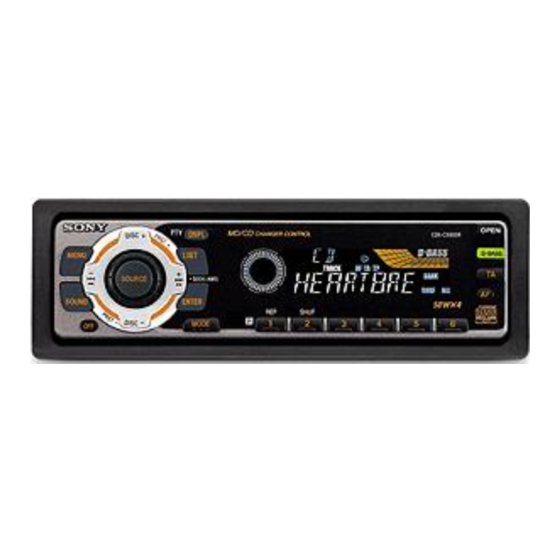
CDX-C4900R/C5000R/C5000RX
SERVICE MANUAL
Ver 1.2 2001. 05
• The tuner and CD sections have no adjustments.
CD player section
Signal-to-noise ratio
90 dB
Frequency response
10 – 20,000 Hz
Wow and flutter
Below measurable limit
Tuner section
FM
Tuning range
87.5 – 108.0 MHz
Aerial terminal
External aerial connector
Intermediate frequency 10.7 MHz/450 kHz
Usable sensitivity
8 dBf
Selectivity
75 dB at 400 kHz
Signal-to-noise ratio
66 dB (stereo),
72 dB (mono)
Harmonic distortion at 1 kHz
0.6% (stereo),
0.3% (mono)
Separation
35 dB at 1 kHz
Frequency response
30 – 15,000 Hz
MW/LW
Tuning range
MW: 531 – 1,602 kHz
LW: 153 – 279 kHz
Aerial terminal
External aerial connector
Intermediate frequency 10.7 MHz/450 kHz
Sensitivity
MW: 30 µV
LW: 40 µV
Power amplifier section
Outputs
Speaker outputs
(sure seal connectors)
Speaker impedance
4 – 8 ohms
Maximum power output 50 W × 4 (at 4 ohms)
Sony Corporation
9-870-070-12
2001E0400-1
e Vehicle Company
© 2001. 5
Shinagawa Tec Service Manual Production Group
Photo: CDX-C5000R
Model Name Using Similar Mechanism
CD Drive Mechanism Type
Optical Pick-up Name
SPECIFICATIONS
General
Outputs
Tone controls
Power requirements
Dimensions
Mounting dimension
Mass
Supplied accessories
*1
Equipped with front and rear outputs:
CDX-C5000RX/C5000R only
Equipped with rear outputs: CDX-C4900R
*2
CDX-C5000RX/C5000R only
Design and specifications are subject to change without
notice.
FM/MW/LW COMPACT DISC PLAYER
AEP Model
UK Model
NEW
MG-383Z-121//Q
KSS-720A
Audio outputs
*1
Power aerial relay control
lead
Power amplifier control
lead
Telephone ATT control
*2
lead
Bass ±9 dB at 100 Hz
Treble ±9 dB at 10 kHz
12 V DC car battery
(negative ground)
Approx. 178 × 50 × 183 mm
(w/h/d)
Approx. 182 × 53 × 162 mm
(w/h/d)
Approx. 1.2 kg
Parts for installation and
connections (1 set)
Front panel case (1)
1
Advertisement
Chapters
Table of Contents

Related Manuals for Sony CDX-C4900R


Summary of Contents for Sony CDX-C4900R
- Page 1 MW/LW Equipped with front and rear outputs: Tuning range MW: 531 – 1,602 kHz CDX-C5000RX/C5000R only LW: 153 – 279 kHz Equipped with rear outputs: CDX-C4900R Aerial terminal External aerial connector CDX-C5000RX/C5000R only Intermediate frequency 10.7 MHz/450 kHz Sensitivity MW: 30 µV Design and specifications are subject to change without LW: 40 µV...
-
Page 2: Table Of Contents
COMPONENTS IDENTIFIED BY MARK 0 OR DOTTED LINE WITH MARK 0 ON THE SCHEMATIC DIAGRAMS AND IN THE PARTS LIST ARE CRITICAL TO SAFE OPERATION. REPLACE THESE COMPONENTS WITH SONY PARTS WHOSE PART NUMBERS APPEAR AS SHOWN IN THIS MANUAL OR IN SUPPLEMENTS PUBLISHED BY SONY. - Page 3 SECTION 1 GENERAL This section is extracted from instruction manual.
-
Page 12: Sub Panel Assy
SECTION 2 DISASSEMBLY Note : Follow the disassembly procedure in the numerical order given. 2-1. SUB PANEL ASSY 4 two claws 6 sub panel assy 2 PTT 2.6x8 3 claw 5 CN500 1 PTT 2.6x8 2-2. CD MECHANISM BLOCK 7 bracket (CD) 5 CD mechanism block 6 PTT 2.6x6 2 PTT 2.6x6... -
Page 13: Main Board
2-3. MAIN BOARD 4 ground point screw 6 MAIN board (PTT 2.6x6) 5 ground point screws (PTT 2.6x6) 3 PTT 2.6x8 2 PTT 2.6x8 1 PTT 2.6x8 2-4. HEAT SINK 6 heat sink 5 PTT 2.6x8 4 PTT 2.6x8 3 PTT 2.6x12 2 PTT 2.6x8 1 PTT 2.6x8... -
Page 14: Chassis (T) Assy
2-5. CHASSIS (T) ASSY 2 P 2x3 3 P 2x3 1 Unsolder the 4 chassis (T) assy lead wires. black white 2-6. LEVER ASSY 5 guide (disc) 6 lever (R) assy 3 tension spring (LR) 7 lever (L) assy 1 PS 2x4 2 DISC IN SW board 4 claws... -
Page 15: Servo Board
2-7. SERVO BOARD 7 PS 2x4 8 PS 2x4 2 CN2 3 Removal the solders. 1 CN3 5 P 2x3 9 SERVO board 4 Removal the solders. 6 loading motor assy (M903) 2-8. ARM ROLLER ASSY • When installing, take note of the positions arm (roller) and washers. -
Page 16: Chassis (Op) Assy
2-9. CHASSIS (OP) ASSY 7 chassis (OP) assy 8 compression spring (FL) 1 tension spring (KF1) 9 compression spring (FL) 2 tension spring (KR1) 5 Fit lever (D) in the direction of the arrow. 6 Turn loading ring in the direction of the arrow. -
Page 17: Diagrams
SECTION 3 DIAGRAMS 3-1. IC PIN DESCRIPTIONS • IC501 CXD2598Q (DIGITAL SERVO, DIGITAL SIGNAL PROCESSOR) (SERVO BOARD) Pin No. Pin Name Pin Description DVDD — Digital power supply pin DVSS — Digital ground SOUT Servo brock serial data output (Not used.) SOCK Servo brock serial data read clock output (Not used.) XOLT... - Page 18 Pin No. Pin Name Pin Description Tracking error signal input Center servo analog input RFDC RF signal input ADIO Test pin (Not used.) AVSSO — Analog ground IGEN Constant current input from OP amplifier. AVDDO — Analog ground ASYO EFM full-swing output (“L”: VSS, “H”: VDD) ASYI Asymmetry comparate voltage input RFAC...
- Page 19 • IC5 CXP84640-063Q (CD SYSTEM CONTROL) (SERVO BOARD) Pin No. Pin Name Pin Description ITRPT — Not used in this set. 2, 3 — — Not used in this set. 4, 5 — Not used in this set. OPEN Front panel open detection input CLOSE Front panel close control output LINKOFF...
- Page 20 Pin No. Pin Name Pin Description SENS SENS signal input — — Not used in this set. — — Not used in this set. BU.IN Back-up power detection input BUSON Bus on control input IN SW Disc in switch input (SW1) SELF SW Self switch input (SW2) SCOR...
- Page 21 Not used. (Open) ILLON Illumination power control output — Power supply pin (+5 V) E2P SIO P SONY-BUS serial data input/output E2P CKO P SONY-BUS serial clock input/output SYSRST SONY-BUS system reset output DOORSW (WRITE OUT) DOOR OPEN/CLOSE detection input (“L”: CLOSE, “H”: OPEN)
- Page 22 Key acknowledge input BUIN Backup voltage detection input ILLIN Illumination (ILLIN) detection input (Fixed at “L” in this set) TELATT Telephone (TEL) detection input (Fixed at “L” in CDX-C4900R) — — Not used. (Open) TEST IN Test mode setting input...
-
Page 23: Block Diagram -Cd Section
CDX-C4900R/C5000R/C5000RX 3-2. BLOCK DIAGRAM — CD SECTION — RF AMP, LD APC, DIGITAL SERVO, OPTICAL PICKUP ERROR AMP DIGITAL SIGNAL PROCESSOR KSS-720A IC501 (Page 24) (Page 24) TUNER LOUT1 CD L RFAC TUNER LOUT2 SECTION CONV. SECTION R-CH RFDC CD SYSTEM CONTROL... -
Page 24: Block Diagram -Tuner Section
CDX-C4900R/C5000R/C5000RX 3-3. BLOCK DIAGRAM — TUNER SECTION — CNJ151–1, –2 CNJ151–3, –4 CNJ151–5, –6 C5000R/C5000RX BUS AUDIO IN AUDIO OUT REAR AUDIO OUT FRONT –1 –2 –3 –4 –5 –6 POWER AMP ELECTRONIC VOLUME IC611 IC151 CN601 FDIL OUT LF FL–... -
Page 25: Block Diagram -Display Section
CDX-C4900R/C5000R/C5000RX 3-4. BLOCK DIAGRAM — DISPLAY SECTION — 3-5. CIRCUIT BOARDS LOCATION SYSTEM CONTROL LCD DRIVE IC501 (3/3) IC901 SUB board KEY MATRIX DISC IN SW board KEY IN0 LCD SO DATA LCD901 LSW901-917 LCD CKO S901-904 KEY IN1 LCD CE... -
Page 26: Printed Wiring Boards -Cd Mechanism Section
CDX-C4900R/C5000R/C5000RX 3-6. PRINTED WIRING BOARDS — CD MECHANISM SECTION — THIS NOTE IS COMMON FOR PRINTED WIRING BOARDS AND SCHEMATIC DIAGRAMS. (In addition to this, the necessary note is printed in each block.) for schematic diagram: • All capacitors are in µF unless otherwise noted. pF: µµF 50 WV or less are not indicated except for electrolytics and tantalums. - Page 27 CDX-C4900R/C5000R/C5000RX • Semiconductor Location Ref. No. Location IC501 Q101 (Page 31)
-
Page 28: Schematic Diagram -Cd Mechanism Section (1/2)
CDX-C4900R/C5000R/C5000RX 3-7. SCHEMATIC DIAGRAM — CD MECHANISM SECTION (1/2) — • Refer to page 39 for IC Block Diagrams. • Waveforms (MODE:PLAY) Approx. 200mVp-p (TE) Approx. 620mVp-p (FE) 1.2Vp-p (RFO) Note: • Voltage and waveforms are dc with respect to ground under no-signal conditions. -
Page 29: Schematic Diagram -Cd Mechanism Section (2/2)
CDX-C4900R/C5000R/C5000RX 3-8. SCHEMATIC DIAGRAM — CD MECHANISM SECTION (2/2) — • Refer to page 40 for IC Block Diagrams. (Page 28) Note: • Voltage is dc with respect to ground under no-signal conditions. no mark : CD PLAY... -
Page 30: Printed Wiring Board -Main Section
CDX-C4900R/C5000R/C5000RX 3-9. PRINTED WIRING BOARD — MAIN SECTION — • Semiconductor Location (Side A) Ref. No. Location D301 D501 D502 D551 J-13 D552 K-13 D553 K-13 D554 J-12 D555 K-13 D556 J-12 D557 K-13 D558 J-12 D559 K-13 D560 J-12... - Page 31 CDX-C4900R/C5000R/C5000RX (Page 27) • Semiconductor Location (Side B) Ref. No. Location H-12 H-11 D-12 D131 F-12 D302 D361 D362 D363 D561 K-11 D562 K-11 D601 D602 D604 D621 B-10 D631 D671 D672 D675 D676 D677 D709 D901 K-12 D902 K-13...
- Page 32 CDX-C4900R/C5000R/C5000RX 3-10. SCHEMATIC DIAGRAM — MAIN SECTION (1/3) — • Refer to page 39 for IC Block Diagrams. (Page 33) (Page 34) Note: • Voltage is dc with respect to ground under no-signal (detuned) condition. no mark : FM ) : MW...
-
Page 33: Schematic Diagram -Main Section (1/3)
CDX-C4900R/C5000R/C5000RX 3-11. SCHEMATIC DIAGRAM — MAIN SECTION (2/3) — (Page 32) Note: • Voltage is dc with respect to ground under no-signal (detuned) condition. no mark : FM ) : MW < > : CD PLAY... -
Page 34: Schematic Diagram -Main Section (3/3)
CDX-C4900R/C5000R/C5000RX 3-12. SCHEMATIC DIAGRAM — MAIN SECTION (3/3) — • Refer to page 39 for IC Block Diagrams. (Page 32) (Page 35) Note: • Voltage is dc with respect to ground under no-signal (detuned) condition. no mark : FM ) : MW <... -
Page 35: Schematic Diagram -Sub (Cd) Section
CDX-C4900R/C5000R/C5000RX 3-13. SCHEMATIC DIAGRAM — SUB (CD) SECTION —... -
Page 36: Printed Wiring Board -Sub (Cd) Section
CDX-C4900R/C5000R/C5000RX 3-14. PRINTED WIRING BOARD — SUB (CD) SECTION — (Page 31) (Page 37) -
Page 37: Printed Wiring Board -Key Section
CDX-C4900R/C5000R/C5000RX 3-15. PRINTED WIRING BOARD — KEY SECTION — • Semiconductor Location Ref. No. Location (D901) A-11 (D902) B-10 (D903) B-10 (D904) B-10 (D951) (D952) (IC901) IC951 LED901 LED902 LED903 LED904 LED910 B-12 LED911 B-12 LED912 A-12 LED913 LED914 LED915... -
Page 38: Schematic Diagram -Key Section
CDX-C4900R/C5000R/C5000RX 3-16. SCHEMATIC DIAGRAM — KEY SECTION — Note: • Voltage is dc with respect to ground under no-signal (detuned) condition. no mark : FM... -
Page 39: Ic Block Diagrams
• IC Block Diagrams IC1 CXA2596M APC PD AMP IC90 BA4558F-E2 HOLD – – OUT1 AGCVTH 23 LC/PD OUT2 –IN1 – APC LD AMP – 22 LD ON +IN1 –IN2 +IN2 21 HOLD SW – 20 AGCCONT – – 19 RF BOT IC701 BA8270F –... - Page 40 IC7 LA6556L-TE-L S-GND INPUT CH2-CH4 OUTPUT 35 MUTE2 MUTE2 ON/OFF CH1 OUTPUT VCC2 34 MUTE1 MUTE1 ON/OFF VL0– 33 VIN4 OUTPUT CONTROL VL0+ 32 VIN4– – VO4+ 31 VIN4+ LEVEL SHIFT VO4– 30 VREF-IN VO3+ 29 VIN1 (VREF)-SW VIN1/VREF SW LEVEL SHIFT VO3–...
- Page 41 IC151 TDA7402TR 32 31 30 29 28 27 26 25 24 23 MONO SUPPLY FADER MIXER SUBWOOFER MONO MONO +PHASE FADER FADER CONTROL ACINLF OUTPUT CONTROL SWINR SWINL MUTE AC OUTR VOICE AC OUTL BANDPASS C-BUS QUAL. QUAL BASS HIGH OUT DIGITAL TRABLE CONTROL...
-
Page 42: Exploded Views
SECTION 4 EXPLODED VIEWS NOTE: • The mechanical parts with no reference • Color Indication of Appearance Parts The components identified by number in the exploded views are not supplied. mark 0 or dotted line with mark. Example : • Items marked “*” are not stocked since 0 are critical for safety. -
Page 43: Front Panel Section
4-2. FRONT PANEL SECTION not supplied (KEY board) LCD901 Ref. No. Part No. Description Remark Ref. No. Part No. Description Remark 3-040-980-01 BUTTON (SOURCE) 3-041-010-01 BUTTON (1-6/M) 3-040-981-01 KNOB (VOL) 3-041-003-01 BUTTON (LIST/ENTER) * 53 3-040-992-01 HOLDER (LCD) 3-040-987-01 BUTTON (OFF) X-3378-398-1 PANEL ASSY, FRONT BACK 3-040-986-01 BUTTON (MENU/SOUND) X-3378-517-1 SUB ASSY, PANEL (C4900R) -
Page 44: Cd Mechanism Section (1)
4-3. CD MECHANISM SECTION (1) (MG-383Z-121//Q) M903 Ref. No. Part No. Description Remark Ref. No. Part No. Description Remark * 101 1-659-836-11 DISC IN SW BOARD * 108 3-039-629-01 BRACKET (MOTOR) * 102 A-3315-034-A CHASSIS (T) ASSY 3-013-388-02 GUIDE (DISC) 3-931-909-01 SPRING (LR), TENSION A-3315-040-A ROLLER ASSY, ARM X-3371-501-1 LEVER (L) ASSY... -
Page 45: Cd Mechanism Section (2)
4-4. CD MECHANISM SECTION (2) (MG-383Z-121//Q) Ref. No. Part No. Description Remark Ref. No. Part No. Description Remark X-3378-956-1 ARM ASSY, CHUCKING 3-931-883-01 SPRING (TR), TENSION 3-931-897-61 DAMPER (T) 3-931-881-01 LEVER (LOCK) 3-039-627-01 LEVER (D) 3-931-882-02 GEAR (MDL) 3-040-165-01 RETAINER (DISC) 3-007-537-11 WHEEL (U), WORM 3-018-272-01 WASHER 3-032-484-01 SPRING (KR1), TENSION... -
Page 46: Cd Mechanism Section (3)
4-5. CD MECHANISM SECTION (3) (MG-383Z-121//Q) M901 M902 The components identified by mark 0 or dotted line with mark. 0 are critical for safety. Replace only with part number specified. Ref. No. Part No. Description Remark Ref. No. Part No. Description Remark X-3378-598-1 CHASSIS (OP) ASSY (INCLUDING M901) -
Page 47: Electrical Parts List
SECTION 5 DISC IN SW ELECTRICAL PARTS LIST NOTE: • Due to standardization, replacements in • Items marked “*” are not stocked since The components identified by mark 0 or dotted line with mark. the parts list may be different from the they are seldom required for routine service. - Page 48 Ref. No. Part No. Description Remark Ref. No. Part No. Description Remark LSW908 1-771-883-21 SWITCH, TACTILE (WITH LED) (MODE) R919 1-216-663-11 METAL CHIP 3.3K 0.5% 1/10W (C5000RX) R920 1-216-667-11 METAL CHIP 4.7K 0.5% 1/10W LSW909 1-762-737-11 SWITCH, KEY BOARD (WITH LED) (D-BASS) R921 1-216-810-11 METAL CHIP 1/16W...
- Page 49 LIMIT SW LOAD SW MAIN Ref. No. Part No. Description Remark Ref. No. Part No. Description Remark < ROTARY ENCODER > 1-163-135-00 CERAMIC CHIP 560PF 1-164-161-11 CERAMIC CHIP 0.0022uF 10% 100V RE901 1-475-014-12 ENCODER, ROTARY 1-163-009-11 CERAMIC CHIP 0.001uF 1-164-315-11 CERAMIC CHIP 470PF <...
- Page 50 MAIN Ref. No. Part No. Description Remark Ref. No. Part No. Description Remark C282 1-163-251-11 CERAMIC CHIP 100PF C673 1-126-157-11 ELECT 10uF C283 1-164-489-11 CERAMIC CHIP 0.22uF C674 1-124-233-11 ELECT 10uF C284 1-162-919-11 CERAMIC CHIP 22PF C675 1-124-233-11 ELECT 10uF C361 1-164-004-11 CERAMIC CHIP 0.1uF...
- Page 51 MAIN Ref. No. Part No. Description Remark Ref. No. Part No. Description Remark D604 8-719-056-82 DIODE UDZ-TE-17-6.2B < JACK > D605 8-719-056-93 DIODE UDZ-TE-17-18B (C5000R/C5000RX) D611 8-719-079-55 DIODE PTZ-TE25-22 1-764-808-21 JACK (ANTENNA) D612 8-719-079-55 DIODE PTZ-TE25-22 J501 1-566-822-41 JACK (REMOTE IN) D613 8-719-079-55 DIODE PTZ-TE25-22 <...
- Page 52 MAIN Ref. No. Part No. Description Remark Ref. No. Part No. Description Remark Q661 8-729-120-28 TRANSISTOR 2SC2412K-T-146-QR R241 1-216-025-11 RES-CHIP 1/10W Q701 8-729-900-53 TRANSISTOR DTC114EKA-T146 R242 1-216-073-00 METAL CHIP 1/10W Q704 8-729-027-23 TRANSISTOR DTA114EKA-T146 R271 1-216-033-00 METAL CHIP 1/10W Q705 8-729-027-23 TRANSISTOR DTA114EKA-T146 R272 1-216-081-00 METAL CHIP...
- Page 53 MAIN SERVO Ref. No. Part No. Description Remark Ref. No. Part No. Description Remark R558 1-216-025-11 RES-CHIP 1/10W < TUNER > R559 1-216-025-11 RES-CHIP 1/10W R560 1-216-025-11 RES-CHIP 1/10W A-3220-738-A TUNER UNIT (TUX-020) R561 1-208-806-11 RES-CHIP 0.5% 1/10W R562 1-208-806-11 RES-CHIP 0.5% 1/10W <...
- Page 54 SERVO Ref. No. Part No. Description Remark Ref. No. Part No. Description Remark C518 1-164-360-11 CERAMIC CHIP 0.1uF R213 1-216-821-11 METAL CHIP 1/16W C519 1-164-360-11 CERAMIC CHIP 0.1uF R301 1-216-843-11 METAL CHIP 1/16W C520 1-164-360-11 CERAMIC CHIP 0.1uF R302 1-216-839-11 METAL CHIP 1/16W C521 1-164-360-11 CERAMIC CHIP...
- Page 55 SERVO SUB (CD) Ref. No. Part No. Description Remark Ref. No. Part No. Description Remark R564 1-216-845-11 METAL CHIP 100K 1/16W MISCELLANEOUS R568 1-216-837-11 METAL CHIP 1/16W *************** R569 1-216-809-11 METAL CHIP 1/16W R570 1-216-821-11 METAL CHIP 1/16W 1-776-527-51 CORD (WITH CONNECTOR) (ISO) (POWER) R572 1-216-809-11 METAL CHIP 1/16W...
- Page 56 CDX-C4900R/C5000R/C5000RX Ver 1.2 2001. 05 Ref. No. Part No. Description Remark PARTS FOR INSTALLATION AND CONNECTIONS *************************************** X-3373-602-1 FRAME ASSY 3-386-828-01 SCREW, FITTING 3-349-410-01 BUSHING X-3366-405-1 SCREW ASSY (EXP), FITTING 3-040-979-01 COLLAR 3-934-325-01 SCREW, +K (5X8) TAPPING 1-465-459-21 ADAPTOR, ANTENNA...
- Page 57 CDX-C4900R/C5000R/C5000RX AEP Model UK Model SERVICE MANUAL SUPPLEMENT-1 File this supplement with the service manual. Subject : Service Notes (ENG-00015, 00016) SERVICE NOTES This product is classified as a CLASS 1 LASER PRODUCT. This label is located on the bottom of the chassis.
- Page 58 CDX-C4900R/C5000R/C5000RX MEMO...
- Page 59 CDX-C4900R/C5000R/C5000RX AEP Model UK Model SERVICE MANUAL SUPPLEMENT-2 File this supplement with the service manual. Subject : Change of Main, Sub (CD) and Key Boards (ECN-CSA01521/CSA02901) TABLE OF CONTENTS 1. CHANGE OF MAIN, SUB (CD) AND KEY BOARDS 1-1. Discrimination ............
-
Page 60: Change Of Main, Sub (Cd) And Key Boards
1. Change of Main, Sub (CD) and Key Boards When performing service and inspection, check the part number of the main, sub (CD) and key boards. 1-1. Discrimination -MAIN BOARD (COMPONENT SIDE)- Main board part No. Former:1-677-055-11 :1-677-055-12 -SUB(CD) BOARD (COMPONENT SIDE)- Sub(CD) board part No. -
Page 61: Diagrams
CDX-C4900R/C5000R/C5000RX 1-2. Diagrams THIS NOTE IS COMMON FOR PRINTED WIRING BOARDS AND SCHEMATIC DIAGRAMS. (In addition to this, the necessary note is printed in each block.) • Refer to page. ) : Refer to page of supplement-2. < > : Refer to page of service manual. -
Page 62: Printed Wiring Board -Main Section
CDX-C4900R/C5000R/C5000RX • PRINTED WIRING BOARD — MAIN SECTION — • Semiconductor Location (Side A) Ref. No. Location D301 D501 D502 D551 J-13 D552 K-13 D553 K-13 D554 J-12 D555 K-13 D556 J-12 D557 K-13 D558 J-12 D559 K-13 D560 J-12... - Page 63 CDX-C4900R/C5000R/C5000RX <Page 27> • Semiconductor Location (Side B) Ref. No. Location H-12 H-11 G-12 D302 D361 D362 D363 D561 K-11 D562 K-11 D601 D602 D604 D621 C-10 D631 D671 D672 D675 D676 D677 D709 IC611 IC671 G-11 Q361 Q362 Q364...
- Page 64 CDX-C4900R/C5000R/C5000RX • SCHEMATIC DIAGRAM — MAIN SECTION (1/3) — • Refer to page 39 of Service manual for IC Block Diagrams. (Page 7) (Page 8) Note: • Voltage is dc with respect to ground under no-signal (detuned) condition. no mark : FM...
-
Page 65: Schematic Diagram -Main Section (1/3)
CDX-C4900R/C5000R/C5000RX • SCHEMATIC DIAGRAM — MAIN SECTION (2/3) — (Page 6) Note: • Voltage is dc with respect to ground under no-signal (detuned) condition. no mark : FM ) : MW < > : CD PLAY ∗ : Impossible to measure... -
Page 66: Schematic Diagram -Main Section (3/3)
CDX-C4900R/C5000R/C5000RX • SCHEMATIC DIAGRAM — MAIN SECTION (3/3) — • Refer to page 39 of Service manual for IC Block Diagrams. (Page 6) (Page 9) Note: • Voltage is dc with respect to ground under no-signal (detuned) condition. no mark : FM ) : MW <... -
Page 67: Schematic Diagram -Sub (Cd) Section
CDX-C4900R/C5000R/C5000RX • SCHEMATIC DIAGRAM — SUB (CD) SECTION —... -
Page 68: Printed Wiring Board -Sub (Cd) Section
CDX-C4900R/C5000R/C5000RX • PRINTED WIRING BOARD — SUB (CD) SECTION — (Page 5) (Page 11) -
Page 69: Printed Wiring Board -Key Section
Ref. No. Location (Page 10) (D901) A-11 LED902 (D902) B-10 LED903 (D903) B-10 LED904 (D904) B-10 LED910 B-12 (D951) LED911 B-12 (D952) LED912 LED913 (IC901) IC951 <Q901> <Q902> LED901 ) : SIDE B < > : SIDE B, CDX-C4900R/C5000R only... -
Page 70: Schematic Diagram -Key Section
CDX-C4900R/C5000R/C5000RX • SCHEMATIC DIAGRAM — KEY SECTION — Note: • Voltage is dc with respect to ground under no-signal (detuned) condition. no mark : FM ∗ : Impossible to measure... -
Page 71: Electrical Parts List
1-3. Electrical Parts List NOTE: • Due to standardization, replacements in • Items marked “*” are not stocked since When indicating parts by reference the parts list may be different from the they are seldom required for routine service. number, please include the board. parts specified in the diagrams or the Some delay should be anticipated components used on the set. - Page 72 Ref. No. Part No. Description Remark Ref. No. Part No. Description Remark LSW911 1-771-476-11 SWITCH, KEY BOARD (WITH LED) (AF) R922 1-216-807-11 METAL CHIP 1/16W (C5000RX) (C4900R/C5000R) LSW912 1-771-610-11 SWITCH, TACTILE (WITH LED) (6) R923 1-216-811-11 METAL CHIP 1/16W (C4900R/C5000R) (C4900R/C5000R) LSW912 1-771-883-11 SWITCH, TACTILE (WITH LED) (6) (C5000RX) R923...
- Page 73 MAIN Ref. No. Part No. Description Remark Ref. No. Part No. Description Remark S903 1-771-884-11 SWITCH, TACTILE (WITH LED) C141 1-163-251-11 CERAMIC CHIP 100PF (SEEK/AMS > M +) C142 1-126-160-11 ELECT S904 1-771-884-11 SWITCH, TACTILE (WITH LED) (DISC-/PRST-) C151 1-162-970-11 CERAMIC CHIP 0.01uF C152 1-124-584-00 ELECT...
- Page 74 MAIN Ref. No. Part No. Description Remark Ref. No. Part No. Description Remark C505 1-164-004-11 CERAMIC CHIP 0.1uF CNJ151 1-774-700-11 JACK, PIN 6P (BUS AUDIO IN, C506 1-163-233-11 CERAMIC CHIP 18PF AUDIO OUT REAR/FRONT) C507 1-163-102-00 CERAMIC CHIP 24PF (C5000R/C5000RX) C509 1-163-021-11 CERAMIC CHIP 0.01uF...
- Page 75 MAIN Ref. No. Part No. Description Remark Ref. No. Part No. Description Remark D705 8-719-056-93 DIODE UDZ-TE-17-18B Q171 8-729-920-21 TRANSISTOR DTC314TK-T-146 D706 8-719-072-70 DIODE MA2ZD14001S0 Q181 8-729-920-21 TRANSISTOR DTC314TK-T-146 D708 8-719-073-01 DIODE MA111-TX Q271 8-729-920-21 TRANSISTOR DTC314TK-T-146 D709 8-719-073-01 DIODE MA111-TX Q281 8-729-920-21 TRANSISTOR DTC314TK-T-146 D710...
- Page 76 MAIN Ref. No. Part No. Description Remark Ref. No. Part No. Description Remark R112 1-216-841-11 METAL CHIP 1/16W R537 1-216-097-11 RES-CHIP 100K 1/10W R121 1-216-049-11 RES-CHIP 1/10W R538 1-216-097-11 RES-CHIP 100K 1/10W R122 1-216-085-00 METAL CHIP 1/10W R539 1-216-097-11 RES-CHIP 100K 1/10W R141...
- Page 77 MAIN SUB (CD) Ref. No. Part No. Description Remark Ref. No. Part No. Description Remark R701 1-216-805-11 METAL CHIP 1/16W LED803 8-719-038-07 LED CL-190PG-CD-T (INSERT MARK) R702 1-216-073-00 METAL CHIP 1/10W (C4900R/C5000R) R703 1-216-025-11 RES-CHIP 1/10W R704 1-216-809-11 METAL CHIP 1/16W <...
- Page 78 CDX-C4900R/C5000R/C5000RX REVISION HISTORY Clicking the version allows you to jump to the revised page. Also, clicking the version at the upper right on the revised page allows you to jump to the next revised page. Ver. Date Description of Revision 2001.
Need help?
Do you have a question about the CDX-C4900R and is the answer not in the manual?
Questions and answers