Sony CDP-M205 Service Manual
Hide thumbs
Also See for CDP-M205:
- Operating instructions manual (38 pages) ,
- Service manual (10 pages)
Table of Contents
Advertisement
Advertisement
Table of Contents

Related Manuals for Sony CDP-M205


Summary of Contents for Sony CDP-M205
- Page 1 CDP-M205/M305 SERVICE MANUAL AEP Model UK Model CDP-M205/M305 E Model CDP-M305 Photo : CDP-M305 Model Name Using Similar Machanism CDP-M201/M301 CD Mechanism Type CDM14-5BD29B Base Unit Type BU-5BD29B Optical Pick-up Type KSS-213B/K-N SPECIFICATIONS COMPACT DISC PLAYER MICROFILM...
-
Page 2: Table Of Contents
OR DOTTED LINE WITH MARK ON THE SCHEMATIC DIAGRAMS AND IN THE PARTS LIST ARE CRITICAL TO SAFE OPERATION. REPLACE THESE COMPONENTS WITH SONY PARTS WHOSE PART NUMBERS APPEAR AS SHOWN IN THIS MANUAL OR IN SERIAL NO. SUPPLEMENTS PUBLISHED BY SONY. -
Page 3: General
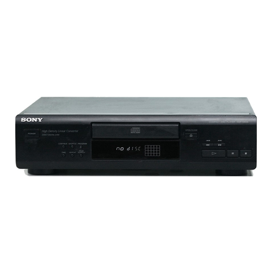
SECTION 1 GENERAL This section is extracted from instruction manual. LOCATION AND FUNCTION OF CONTROLS Front Panel !§ 7 !∞ !¢ !£ !™ !¡ 1 POWER switch P(PAUSE) button ·(PLAY) button 2 CONTINUE button !¡ 3 SHUFFLE button DISPLAY window !™... -
Page 4: Servicing Note
SECTION 2 SERVICING NOTE HOW TO OPEN THE DISC TRAY WHEN POWER SWITCH TURNS OFF 1 Turn in the direction of the arrow Caution : When you work, keep the set horizontal. – 4 –... -
Page 5: Disassembly
SECTION 3 DISASSEMBLY Note : Follow the disassembly procedure in the numerical order given. 3-1. PANEL, FRONT REMOVAL Panel, Front Panel, Loading 4 Two screws (+BVTP 3x8TYPE2 N-S) 3 Wire (Flat type) (21core) 1 Turn in the direction of the arrow (Refer to page 4) 3-2. -
Page 6: Electrical Adjustments
SECTION 4 ELECTRICAL ADJUSTMENTS E-F Balance (1 Track Jump) check CD SECTION oscilloscope Note: BD board 1. CD Block is basically constructed to operate without adjustment. Therefore, check each item in order given. TP (TEO) 2. Use YEDS-18 disc (3-702-101-01) unless otherwise indicated. TP (VC) 3. -
Page 7: Diagrams
SECTION 5 DIAGRAMS 5-1. IC PIN FUNCTION IC101 FOCUS/TRACKING/SLED SERVO RF AMP (CXA1992AR) Pin No. Pin name Description. Focus error amplifier output. Connected internally to the window comparator input for bias adjustment. Focus error input. FDFCT Capacitor connection pin for defect time constant. Ground this pin through a capacitor for cutting the focus servo high-frequency gain. - Page 8 Pin No. Pin name Description. F I-V and E I-V amplifier inverted input. Connect these pins to photo diodes F and E. I-V amplifier E gain adjustment – (When not using automatic balance adjustment) (not used). – Negative power supply. Tracking error amplifier output E-F signal is output.
- Page 9 Pin No. Pin name Description. VCTL VCO2 control voltage input Charge-pump output to master PLL FILO Filter output to master PLL FILI Filter input for master PLL AVSS – Analog ground CLTV Control voltage input for VCO AVDD – Analog power supply EFM signal input BIAS Asymmetry circuit constant current input...
- Page 10 Pin No. Pin name Description. XVSS – Master clock ground AVSS – Analog ground LOUT2 Rch line output AIN2 Rch opamp input AOUT2 Rch analog output AVDD – Analog power supply AVSS – Analog ground — – Not used — –...
- Page 15 BLOCK DIAGRAMS IC102 BA5941FP – + – + – LEVEL SHIFT LEVEL SHIFT LEVEL SHIFT – LEVEL SHIFT – + – + – – – MUTE IC103 CXD2529Q 80 79 78 77 76 75 74 73 72 71 70 69 68 67 66 65 64 63 62 61 60 59 58 57 56 55 54 53 52 51 LRCK AVSS WDCK...
- Page 16 IC101 CXA1992AR – RF SUMMING PD2 IV PD1 IV FE_BIAS SENS2 ↓ SENS1 – LASER POWER CONTROL F IV AMP FE AMP – C. OUT E IV AMP – DFCT XRST – LEVEL S DATA FO. BIAS WINDOW MIRR COMP. ↓...
-
Page 17: Exploded Views
* 13 A-4699-609-A MAIN BOARD, COMPLETE (Singapore) 4-977-588-11 PANEL, LOADING (M205) * 14 4-954-051-51 HOLDER, PC BOARD 3-008-600-01 EMBLEM (5-AR), SONY X-3371-435-1 FOOT (SMALL) ASSY 1-773-147-11 WIRE (FLAT TYPE) (21 CORE) 4-988-717-01 PANEL, FRONT (M305) 4-988-717-11 PANEL, FRONT (M205) * 17... -
Page 18: Cd Block Section
6-2. CD BLOCK SECTION (including p A) BU-5BD29 M151 Ref. No. Part No. Description Remark Ref. No. Part No. Description Remark ––––––– ––––––– –––––––––– ––––––– ––––––– ––––––– –––––––––– –––––– 4-933-112-01 TABLE, DISC 4-933-134-01 SCREW (+PTPWH M2.6X6) 4-933-110-41 HOLDER (MG) * 53 1-452-879-11 MAGNET 4-959-996-01 SPRING (932), COMPRESSION 4-933-109-01 CAM... -
Page 19: Optical Pick-Up Block Section (Bu-5Bd29B)
6-3. OPTICAL PICK-UP BLOCK SECTION (BU-5BD29B) M101 M102 The components identified by mark ! or dotted line with mark ! are critical for safety. Replace only with part number specified. Ref. No. Part No. Description Remark Ref. No. Part No. Description Remark –––––––... -
Page 20: Electrical Parts List
SECTION 7 ELECTRICAL PARTS LIST NOTE : SEMICONDUCTORS Due to standardization, replacements in the In each case, u : µ , for example : The components identified by mark ! parts list may be different from the parts speci- uA..: µ A.., uPA..: µ PA..or dotted line with mark ! are critical fied in the diagrams or the components used on uPB.. - Page 21 LOADING MAIN Ref. No. Part No. Description Remark Ref. No. Part No. Description Remark ––––––– ––––––– –––––––––– ––––––– ––––––– ––––––– –––––––––– –––––– R116 1-216-061-00 METAL CHIP 3.3K 1/10W 1-645-721-11 LOADING BOARD ************** R117 1-216-069-00 METAL CHIP 6.8K 1/10W R118 1-216-063-91 METAL GLAZE 3.9K 1/10W <...
- Page 22 MAIN Ref. No. Part No. Description Remark Ref. No. Part No. Description Remark ––––––– ––––––– –––––––––– ––––––– ––––––– ––––––– –––––––––– –––––– C906 1-101-006-00 CERAMIC 0.047uF R306 1-249-413-11 CARBON 1/4W C907 1-101-006-00 CERAMIC 0.047uF R307 1-249-432-11 CARBON 1/4W C908 1-101-006-00 CERAMIC 0.047uF R308 1-247-891-00 CARBON...
- Page 23 CDP-M205/M305 PANEL Ref. No. Part No. Description Remark Ref. No. Part No. Description Remark ––––––– ––––––– –––––––––– ––––––– ––––––– ––––––– –––––––––– –––––– A-4699-606-A PANEL BOARD, COMPLETE (M205) S506 1-554-303-21 SWITCH, TACTILE (SHUFFLE) A-4699-607-A PANEL BOARD, COMPLETE (M305) S507 1-554-303-21 SWITCH, TACTILE (CONTINUE) S508 1-554-303-21 SWITCH, TACTILE (OPEN/CLOSE§)
Need help?
Do you have a question about the CDP-M205 and is the answer not in the manual?
Questions and answers