Harman Kardon AVR245 Service Manual
7 x 50w 7.1 channel a/v receiver
Hide thumbs
Also See for AVR245:
- Owner's manual (76 pages) ,
- Worksheet (3 pages) ,
- Quick start manual (2 pages)
Table of Contents
Advertisement
Quick Links
harman/kardon
7 X 50W 7.1 CHANNEL A/V RECEIVER
Esd Warning.....................................2
Leakage Testing...............................3
Basic Specifications.......................4
Packaging........................................5
Front Panel Controls.....................6
Rear Panel Connections................8
Remote Control Functions..........11
Connections/Installation.............14
Operation.......................................25
Troubleshooting Guide.................32
REMOTE & PROCESSOR RESETS..........33
AVR245
SERVICE MANUAL
CONTENTS
harman/kardon, Inc.
250 Crossways Park Dr.
Woodbury, New York 11797
Disassembly.....................................34
Unit Exploded View..........................38
Exploded View Parts List...............39
AMP BIAS ADJUSTMENT......................40
Block Diagram................................41
Pcb Drawings.................................42
Electrical Parts List....................53
Semiconductor Pinouts................97
Schematics....................................220
WIRING DIAGRAM..............................228
Rev 0 1/2007
Advertisement
Table of Contents

Related Manuals for Harman Kardon AVR245


Summary of Contents for Harman Kardon AVR245
-
Page 1: Service Manual
AVR245 7 X 50W 7.1 CHANNEL A/V RECEIVER SERVICE MANUAL CONTENTS ESD WARNING……………………………….2 DISASSEMBLY……………………………….34 LEAKAGE TESTING……………….…..…..3 UNIT EXPLODED VIEW…………..…….…..38 BASIC SPECIFICATIONS…………………..4 EXPLODED VIEW PARTS LIST……………39 PACKAGING…………………………….……5 AMP BIAS ADJUSTMENT……………….…40 FRONT PANEL CONTROLS………..…..…..6 BLOCK DIAGRAM…………………………..41 REAR PANEL CONNECTIONS………….…8 PCB DRAWINGS……………………………42 REMOTE CONTROL FUNCTIONS……….11... - Page 2 AVR245 Some semiconductor (solid state) devices can be damaged easily by static electricity. Such components commonly are called Electrostatically Sensitive (ES) Devices. Examples of typical ES devices are integrated circuits and some field effect transistors and semiconductor "chip" components.
- Page 3 AVR245 SAFETY PRECAUTIONS The following check should be performed for the continued protection of the customer and service technician. LEAKAGE CURRENT CHECK Measure leakage current to a known earth ground (water pipe, conduit, etc.) by connecting a leakage current tester...
- Page 4 All features and specifications are subject to change without notice. Transient Intermodulation Distortion (TIM) Unmeasurable Harman Kardon, Harman International, EzSet+ and Logic 7 are trademarks of Harman International Industries, Bridge Slew Rate 40V/µsec Incorporated, registered in the United States and/or other countries.
- Page 5 AVR245 CPS5A564 CPS5A565...
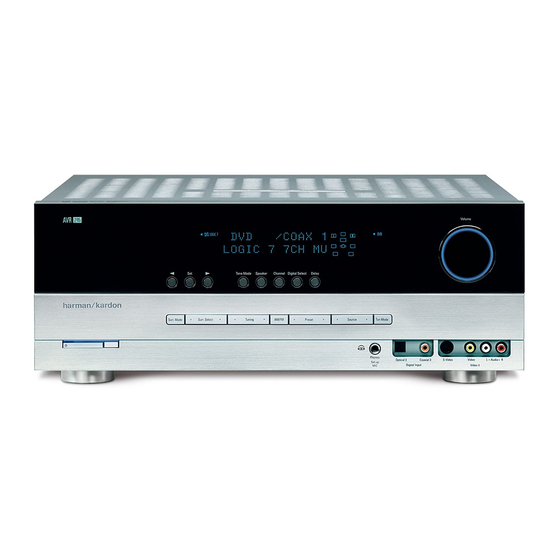
- Page 6 AVR245 FRONT-PANEL CONTROLS Main Power Switch: Surround Mode: This is a mechanical switch that turns the Press this button to select a surround sound (e.g., power supply on or off. It is usually left pressed in (On position), and multichannel) mode group.
- Page 7 AVR245 Source Digital Input Message Display Speaker Size Indicators Select Tone Mode Setup Speaker/Channel Channel Level Navigation Surround Mode Indicators Delay Volume Input Indicators Adjust Headphone Power Surround Tuning Preset Stations Digital Analog Audio Jack/Ezet+ Indicator Mode Audio Inputs...
- Page 8 Input). When several source devices are used, connect them in “daisy The Bridge/DMP Input: Connect the optional Harman Kardon Bridge chain” fashion. to this input for use with your iPod (not included). Make...
- Page 9 AVR 245’s on-screen displays. RS-232 Serial Port: This specialized connector may be used with your personal computer in case Harman Kardon offers a software upgrade for the receiver at some time in the future. RS-232 Mode: Leave this switch popped out in the Operate position unless the AVR 245 is being upgraded.
- Page 10 AVR245 Component Coaxial Digital Video Video 3 Audio Video 1 Inputs Inputs RS-232 DVD A/V Antenna RS-232 AC Power (1, 2 & 3) Serial Port Inputs Inputs Jack (1 & 2) Reset Cord FM Antenna Outputs Component HDMI HDMI 2...
-
Page 11: Remote Control Functions
AVR245 REMOTE CONTROL FUNCTIONS The AVR 245 remote is capable of controlling 11 devices, including the IR Transmitter Lens: As buttons are pressed on the remote, AVR itself and an iPod docked in the optional The Bridge accessory. infrared codes are emitted through this lens. Make sure it is pointing During the installation process, you may program the codes for each toward the component being operated. - Page 12 AVR245 IR Transmitter Lens Power On Mute Program Indicator Power Off AVR Selector Input Selectors AM/FM 6-Channel Input Selector XM Radio Test Tone TV/Video Sleep Volume Control DSP Surround Not Used On-Screen Display Speaker Setup Channel Level Digital Input...
-
Page 13: Night Mode
AVR245 REMOTE CONTROL FUNCTIONS Channel Level: Tuning: Press this button to adjust the output levels for each Press these buttons to tune a radio station or XM Radio chan- channel so that all speakers sound equally loud at the listening position. -
Page 14: Connecting Source Devices To The Avr
AVR245 CONNECTIONS There are different types of audio and video connections used to con- Bare wire cables are installed as follows (see Figure 2): nect the receiver to the speakers and video display, and to connect 1. Unscrew the terminal cap until the pass-through hole in the collar is the source devices to the receiver. -
Page 15: Audio Connections
Figure 8 – The Bridge Figure 5 – Optical Digital Audio Harman Kardon receivers also include a proprietary, dedicated audio Due to the nature of digital signals as binary bits, they aren’t subject connection called “The Bridge/DMP”. If you own an iPod with a dock to signal degradation the way analog signals are. -
Page 16: Digital Video Connections
The RS-232 serial port on the AVR 245 is used only for data. If Figure 10. Harman Kardon releases a software upgrade for the receiver’s operating system at some time in the future, the upgrade may be downloaded to the AVR using this port. Complete instructions will be provided at Composite that time. -
Page 17: Connections/Installation
AVR245 INSTALLATION You are now ready to connect your various components to your receiver. Step Three – Connect the Antennas Before beginning, make sure that all components, including the AVR 245, Connect the FM and AM antennas to their terminals. See Figure 19. - Page 18 AVR245 INSTALLATION NOTE: It’s possible for a source to use none of the connections We recommend connecting your various sources using the connections named for that source. For example, you might connect your shown in Table 2 (below) in order to simplify programming your receiver DVD player to the Component Video 1 inputs and the Coax 1 and remote control.
- Page 19 AVR245 INSTALLATION NOTE: The AVR 245 is equipped with a total of six digital audio inputs, four on the rear panel (Coaxial 1 and 2, Optical 1 and 2) and two on the front panel (Coaxial 3 and Optical 3). However, there are a total of nine sources that may be connected to devices that have digital audio outputs.
- Page 20 AVR245 INSTALLATION HDMI 2 Source The DVD source is used for a DVD player. If you have a more advanced The HDMI 2 source is used with a second device that is capable of out- multichannel device, such as a Blu-ray Disc or HD-DVD player, you may putting digital video through an HDMI connection, such as an HD-DVD connect it to the DVD source.
- Page 21 Bridge or component video, connect the S-video Monitor output on the receiver With Harman Kardon’s optional The Bridge, you can listen to audio to an S-video input on your display. See Figure 33. Make a note of how the input is labeled.
- Page 22 The AVR 245’s remote is factory-programmed to control an iPod docked in The Bridge and many Harman Kardon DVD and CD players. If you have other source devices in your system, follow these steps to...
- Page 23 However, you may still connect the source to the AVR 245 and operate it using the device’s original remote control. Alternatively, you may wish to consider purchasing Harman Kardon’s optional TC 30 activity-based remote, which is programmed by accessing a large data- Figure 38 –...
- Page 24 AVR245 INSTALLATION Figure 39 – AVR and Input Selectors NOTE: Any time you press one of the Input Selectors on the remote (i.e., DVD/CD, TAPE/The Bridge, HDMI 1/HDMI 2, VID1, VID2, VID3 or VID4), the remote will switch modes so that it will only transmit the codes programmed to operate that device.
-
Page 25: Operation
AVR245 OPERATION Now that you have installed your system components and completed at example, if you will be on vacation), it is not necessary to turn off the least a basic configuration of your receiver, you are ready to begin Master Power Switch. -
Page 26: Mute Function
AVR245 OPERATION Mute Function NOTE: The AVR 245 does not have a conventional balance control. The EzSet+ process compensates for any characteris- To temporarily mute all speakers and the headphones, press the Mute tics of your room or speakers, and we recommend that you Button on the remote. - Page 27 AVR245 OPERATION The Bridge sources, and the HDMI 1 and HDMI 2 sources. The first source, the Component Video 2 input is assigned to the Video 1 source, press of any of these three Input Selectors will select the source whose and the Component Video 3 input is assigned to the Video 2 source.
-
Page 28: Using The Tuner
AVR245 OPERATION source. If your video display doesn’t have component video inputs, NOTE: The 6-/8-Channel Inputs pass the incoming signals then connect the player’s composite or S-video output to the DVD’s directly to the volume control, without digitizing or processing corresponding video input. -
Page 29: Xm Radio Operation
AVR245 OPERATION FM station has been tuned, pressing the Tuning Mode Button will switch You should be able to tune in Channel 1, the Preview Channel, to con- between stereo and mono tuning, which may improve reception of firm that your equipment is ready for activation. There are three ways to weaker stations. -
Page 30: The Bridge
AVR245 OPERATION Recording Figure 73 – Using The Bridge (Remote) Two-channel analog and digital audio signals, as well as composite and S-video signals, are normally available at the appropriate recording outputs. Thus, to make a recording, you need only make sure to con-... -
Page 31: Selecting A Surround Mode
AVR245 OPERATION Selecting a Surround Mode Surround mode selection can be as simple or sophisticated as your individual system and tastes. Feel free to experiment with the many available surround modes on the AVR 245, and you may find a few that become your favorites for certain sources or program types. -
Page 32: Troubleshooting Guide
• Amplifier is in protection mode • Contact your local Harman Kardon service center due to internal problems No sound from surround or • Incorrect surround mode • Select a mode other than Stereo center speakers •... - Page 33 RESET message appears in the display. If the receiver still does not function correctly after a processor reset, contact an authorized Harman Kardon service center for assistance. Service centers may be located by visiting our Web site at www.harmankardon.com.
-
Page 34: Disassembly
DISASSEMBLY harman/kardon AVR245 AVR245 1. Removing the Top Cabinet 3. Removing the Rear Panel Remove the Screws Remove the Screws 24 25 20 21 30 31 4. Removing the Main PCB Remove the Screws 2. Removing the Front Panel Remove the Screws... - Page 35 AVR245 AVR245 DISASSEMBLY PROCEDURE 1 TOP-CABINET(21) REMOVAL 1. Remove 13 screws (S1,S7) and then remove the Top-cabinet. 2 FRONT PANEL ASS’Y REMOVAL 1. Remove the Top-cabinet, referring to the previous step 1 . 2. Disconnect the card cable between connector (CN72-17p) on the Fip PCB (37-1) and connector (CN72) on the Input PCB (39-1).
- Page 36 AVR245 7 KEY PCB (37-2) REMOVAL 1. Remove the Top-cabinet, referring to the previous step 1 . 2. Remove the Front Panel ASS’Y, referring to the previous step 2 . 3. Remove the Fip PCB (37-1), referring to the previous step 6 .
- Page 37 AVR245 5. Disconnect the lead wire (BN85-2P) on the Xm PCB (43) from connector (CN85) on the Regulator PCB (A)(40-2). 6. Remove 1 screws (S15) and then remove the xm PCB (43). 14 INPUT PCB (39-1) REMOVAL 1. Remove the Top-cabinet, referring to the previous step 1 .
- Page 38 AVR245 37-7 40-3 40-1 40-4 39-2 39-1 40-5 40-2 38-1 39-5 40-7 40-2 DESCRIPTION PARTS NO. Q,ty REMARK ORNAMENT,VOLUME CGU1A318Z CAP,VOLUME CGX1A338MBB13 HOLDER,VOLUME CMH1A214 INDICATOR,VOLUME CGL1A222 WINDOW ASS'Y CGUAVR245 WINDOW,FIP CGU1A399Z BADGE,MODEL CGB1A169Z SHEET,VOLUME CMZ2A090 FILTER,FIP CMZ1A088 BDAGE,HARMAN/KARDON KGB1A158Z...
- Page 39 AVR245...
- Page 40 AVR245 AMPLIFIER SECTION BIAS ADJUSTMENT Measurement condition .No input signal or volume position is minimum. Standard value .Ideal current = 48mA (± 5%) .Ideal DC Voltage = 25.92mV (± 5%) DC EVM CUP11911Y (MAIN PCB) CN66 CN61 CN64 CN63...
- Page 41 AVR245...
- Page 42 AVR245...
- Page 43 AVR245...
- Page 44 AVR245...
- Page 45 AVR245...
- Page 46 AVR245...
- Page 47 AVR245...
- Page 48 AVR245...
- Page 49 AVR245...
- Page 50 AVR245...
- Page 51 AVR245...
- Page 52 AVR245...
- Page 53 AVR245 AVR245 Electrical Parts List Ref. Designator Part Number Description FRONT PCB ASSY CUP11910-1 Capacitors C714 HCBS1H151KBT CAP , CERAMIC 150UF 50V K C716 CCEA1AH331T CAP , ELECT 330UF 10V C723 HCBS1H104ZFT CAP , CERAMIC 0.1UF 50V Z C728...
- Page 54 AVR245 Ref. Designator Part Number Description FRONT PCB ASSY CUP11910-1 R892 CRD20TJ222T RES , CARBON 2.2K OHM 1/5W J R893 CRD20TJ333T RES , CARBON 33K OHM 1/5W J R913 CRD20TJ102T RES , CARBON 1K OHM 1/5W J R915 CRD20TJ473T...
- Page 55 AVR245 Ref. Designator Part Number Description PCB , FRONT PANEL KEY CUP11910-2 R755 CRD20TF1801T RES , CARBON 1.8K /1/5W /F R756 CRD20TF2701T RES , CARBON 2.7K /1/5W/F R757 CRD20TF3301T RES ,CARBON 3.3K /1/5W/F R758 CRD20TF5601T RES ,CARBON(5.6K/F) 5.6K/1/5W/F R759...
- Page 56 AVR245 Ref. Designator Part Number Description PCB , VR JACK CUP11910-6 C843 CCEA1HH100T CAP , ELECT 10UF 50V C855 HCBS1H101KBT CAP , CERAMIC 100PF 50V K C856 HCBS1H101KBT CAP , CERAMIC 100PF 50V K C857 HCBS1H104ZFT CAP , CERAMIC 0.1UF 50V Z...
- Page 57 AVR245 Ref. Designator Part Number Description PCB , VR JACK CUP11910-6 BN92 CWB2B905100EN WIRE ASS'Y WIRE PCB , PHONE JACK CUP11910-5 Capacitors C807 HCBS1H104ZFT CAP , CERAMIC 0.1UF 50V Z C808 HCBS1H181KBT CAP , CERAMIC 180PF 50V Z C809...
- Page 58 AVR245 Ref. Designator Part Number Description PCB , PHONE JACK CUP11910-5 R905 CRD20TJ104T RES , CARBON 100K OHM 1/5W J R906 CRD20TJ104T RES , CARBON 100K OHM 1/5W J R907 CRD20TJ472T RES , CARBON 4.7K OHM 1/5W J R908...
- Page 59 AVR245 Ref. Designator Part Number Description MAIN PCB/HEATSINK (CUP11911Z) C605 CCCT1H120JC CAP , CERAMIC 12PF 50V C606 CCCT1H330JC CAP , CERAMIC 33PF 50V C607 CCCT1H330JC CAP , CERAMIC 33PF 50V C608 CCCT1H330JC CAP , CERAMIC 33PF 50V C609 CCCT1H330JC...
- Page 60 AVR245 Ref. Designator Part Number Description MAIN PCB/HEATSINK (CUP11911Z) C950 CCEA1AH471T CAP , ELECT 470UF 10V C971 HCQI1H562JZT CAP , MYLAR 5600PF 50V C972 HCQI1H562JZT CAP , MYLAR 5600PF 50V C973 HCQI1H562JZT CAP , MYLAR 5600PF 50V C974 HCQI1H562JZT...
- Page 61 AVR245 Ref. Designator Part Number Description MAIN PCB/HEATSINK (CUP11911Z) D912 CVD1SS133MT DIODE 1SS133 D914 CVD1SS133MT DIODE 1SS133 D917 CVD1SS133MT DIODE 1SS133 D953 CVD1SS133MT DIODE 1SS133 D954 CVD1N4003SRT RECT , DIODE 1N4003 D955 CVD1N4003SRT RECT , DIODE 1N4003 D956 CVD1N4003SRT...
- Page 62 AVR245 Ref. Designator Part Number Description MAIN PCB/HEATSINK (CUP11911Z) Q682 HVTKSC2785YT TRANSISTOR NPN KSC2785Y Q683 HVTKSC2785YT TRANSISTOR NPN KSC2785Y Q684 HVTKSC2785YT TRANSISTOR NPN KSC2785Y Q685 HVTKSC2785YT TRANSISTOR NPN KSC2785Y Q801 HVTKSC2785YT TRANSISTOR NPN KSC2785Y Q802 HVTKSC2785YT TRANSISTOR NPN KSC2785Y...
- Page 63 AVR245 Ref. Designator Part Number Description MAIN PCB/HEATSINK (CUP11911Z) IC94 HVIMC7805C I.C, REGULATOR KA7805-ABTU IC97 HVIS-80842CNY-X I.C RESET S-80842CNY-X Resistors R501 CRD20TJ433T RES , CARBON 43K OHM 1/5W J R502 CRD20TJ433T RES , CARBON 43K OHM 1/5W J R503...
- Page 64 AVR245 Ref. Designator Part Number Description MAIN PCB/HEATSINK (CUP11911Z) R568 CRD20TJ561T RES , CARBON 560 OHM 1/5W J R569 CRD20TJ561T RES , CARBON 560 OHM 1/5W J R570 CRD20TJ561T RES , CARBON 560 OHM 1/5W J R571 CRD20TJ561T RES , CARBON...
- Page 65 AVR245 Ref. Designator Part Number Description MAIN PCB/HEATSINK (CUP11911Z) R648 CRD25FJ3R3T RES , CARBON 3.3 OHM 1/4W J R649 CRD25FJ3R3T RES , CARBON 3.3 OHM 1/4W J R650 CRD25FJ3R3T RES , CARBON 3.3 OHM 1/4W J R651 CRD25FJ3R3T RES , CARBON 3.3 OHM 1/4W J...
- Page 66 AVR245 Ref. Designator Part Number Description MAIN PCB/HEATSINK (CUP11911Z) R807 CRD20TJ911T RES , CARBON 910 OHM 1/5W J R808 CRD20TJ182T RES , CARBON 1.8K OHM 1/5W J R809 CRD20TJ182T RES , CARBON 1.8K OHM 1/5W J R812 CRD25TJ470T RES , CARBON...
- Page 67 AVR245 Ref. Designator Part Number Description MAIN PCB/HEATSINK (CUP11911Z) R908 CRD20TJ105T RES , CARBON 1M OHM 1/5W J R909 CRD20TJ682T RES , CARBON 6.8K OHM 1/5W J R910 CRD20TJ105T RES , CARBON 1M OHM 1/5W J R911 CRD25TJ680T RES , CARBON...
- Page 68 AVR245 Ref. Designator Part Number Description MAIN PCB/HEATSINK (CUP11911Z) R991 CRD20TJ822T RES , CARBON 8.2K OHM 1/5W J R992 CRD20TJ562T RES , CARBON 5.6K OHM 1/5W J R998 CRD20TJ103T RES , CARBON 10K OHM 1/5W J R656 CRF5EKR27HX2K RES , CEMENT 0.27ohm X 2...
- Page 69 AVR245 Ref. Designator Part Number Description MAIN PCB/HEATSINK (CUP11911Z) JW90 CWE8212120VV WIRE , RED WIRE JW91 CWE8212180VV WIRE ASS'Y WIRE JW93 CWEP202110VV WIRE WIRE L501 CLEY0R5KAK COIL , SPEAKER 0.5UH L502 CLEY0R5KAK COIL , SPEAKER 0.5UH L503 CLEY0R5KAK COIL , SPEAKER 0.5UH...
- Page 70 AVR245 Ref. Designator Part Number Description PCB , POWER TRANS CUP11916-3,4 C109 CCFT1H104ZF CAP , SEMICONDUCTOR 0.1UF 50V ZF C117 CCEA1HH4R7T CAP , ELECT 4.7UF 50V C118 HCBS1H103ZFT CAP , CERAMIC 0.01UF 50V C119 CCEA1JH470TS CAP , ELECT 63V/47UF/105'C...
- Page 71 AVR245 Ref. Designator Part Number Description PCB , POWER TRANS CUP11916-3,4 HVDKBU804F DIODE , BRIDGE BRIDGE DIODE Q104 HVTKSC2316YT TRANSISTOR NPN KSC2316Y Q911 HVTKTA1267YT TRANSISTOR PNP KTA1267Y Q912 HVTKTC3198YT TRANSISTOR NPN KTC3198Y Q913 HVTKTC3198YT TRANSISTOR NPN KTC3198Y Resistors R101...
- Page 72 AVR245 Ref. Designator Part Number Description PCB , DIGITAL IN/OUT CUP11916-1 C756 CCFT1H104ZF CAP , SEMICONDUCTOR 0.1UF 50V ZF C757 CCFT1H104ZF CAP , SEMICONDUCTOR 0.1UF 50V ZF C759 HCBS1H101KBT CAP , CERAMIC 100PF 50V C760 CCFT1H473ZF CAP, CERAMIC 0.047UF 50V ZF...
- Page 73 AVR245 Ref. Designator Part Number Description PCB , BIAS TR CUP11916-2 R879 CRD20TJ331T RES , CARBON 330 OHM 1/5W J R880 CRD20TJ331T RES , CARBON 330 OHM 1/5W J R882 CRD20TJ122T RES , CARBON 1.2K OHM 1/5W J R883...
- Page 74 AVR245 Ref. Designator Part Number Description PCB , REGULATOR CUP11916-5,6 R913 CRD20TJ153T RES , CARBON 15K OHM 1/5W J CN85 CJP02GA01ZY WAFER, STRAIGHT, 2PIN WAFER CN89 CJP02GA01ZY WAFER, STRAIGHT, 2PIN WAFER CN95 CJP03GA19ZY WAFER, STRAIGHT, 3PIN WAFER CN96 CJP09GA01ZY...
- Page 75 AVR245 Ref. Designator Part Number Description PCB , INPUT CUP11912-1 C307 CCUS1H471JA CAP , CHIP 470PF C308 CCUS1H471JA CAP , CHIP 470PF C309 CCUS1H332KC CAP , CHIP 3300PF C310 CCUS1H332KC CAP , CHIP 3300PF C311 CCUS1H332KC CAP , CHIP...
- Page 76 AVR245 Ref. Designator Part Number Description PCB , INPUT CUP11912-1 C396 CCUS1H151JA CAP , CHIP 150PF C397 CCUS1H151JA CAP , CHIP 150PF C398 CCUS1H151JA CAP , CHIP 150PF C601 CCUS1H104KC CAP , CHIP 0.1UF C603 CCUS1H104KC CAP , CHIP 0.1UF...
- Page 77 AVR245 Ref. Designator Part Number Description PCB , INPUT CUP11912-1 C769 CCUS1H104KC CAP , CHIP 0.1UF C770 CCUS1H104KC CAP , CHIP 0.1UF C771 CCUS1H104KC CAP , CHIP 0.1UF C772 CCUS1H104KC CAP , CHIP 0.1UF C773 CCUS1H104KC CAP , CHIP 0.1UF...
- Page 78 AVR245 Ref. Designator Part Number Description PCB , INPUT CUP11912-1 C612 CCEA1CH101T CAP , ELECT 100UF 16V C614 CCEA1CH101T CAP , ELECT 100UF 16V C616 CCEA1CH101T CAP , ELECT 100UF 16V C618 CCEA1CH101T CAP , ELECT 100UF 16V C620...
- Page 79 AVR245 Ref. Designator Part Number Description PCB , INPUT CUP11912-1 IC34 HVINJM2068MDTE1 I.C , DUAL OP AMP IC72 HVI74HCU04AFNG I.C , INVERTER TOSHIBA IC73 HVIAK4589VQ-T I.C , CODEC + DIR ASAHI KASEI IC75 CVICS49510-CQ I.C , DSP CIRRUS LOGIC...
- Page 80 AVR245 Ref. Designator Part Number Description PCB , INPUT CUP11912-1 RN85 CRJ104DJ330T RES , 4ARRAY (1608*4) 33 OHM/1608*4 RN86 CRJ104DJ103T RES , 4ARRAY (1608*4) 10K OHM/1608*4 RN87 CRJ104DJ330T RES , 4ARRAY (1608*4) 33 OHM/1608*4 RN88 CRJ104DJ103T RES , 4ARRAY (1608*4)
- Page 81 AVR245 Ref. Designator Part Number Description PCB , INPUT CUP11912-1 R254 CRJ10DJ4R7T RES , CHIP 4.7 OHM R255 CRJ10DJ4R7T RES , CHIP 4.7 OHM R256 CRJ10DJ4R7T RES , CHIP 4.7 OHM R257 CRJ10DJ4R7T RES , CHIP 4.7 OHM R258...
- Page 82 AVR245 Ref. Designator Part Number Description PCB , INPUT CUP11912-1 R321 CRJ10DJ512T RES , CHIP 5.1K OHM R322 CRJ10DJ122T RES , CHIP 1.2K OHM R323 CRJ10DJ122T RES , CHIP 1.2K OHM R324 CRJ10DJ512T RES , CHIP 5.1K OHM R325...
- Page 83 AVR245 Ref. Designator Part Number Description PCB , INPUT CUP11912-1 R398 CRJ10DF3920T RES. CHIP (392R 1%) 392 OHM R701 CRJ10DJ103T RES , CHIP 10K OHM R702 CRJ10DJ103T RES , CHIP 10K OHM R709 CRJ10DJ103T RES , CHIP 10K OHM...
- Page 84 AVR245 Ref. Designator Part Number Description PCB , INPUT CUP11912-1 R785 CRJ10DJ104T RES , CHIP 100K OHM R786 CRJ10DJ471T RES , CHIP 470 OHM R787 CRJ10DJ103T RES , CHIP 10K OHM R788 CRJ10DJ103T RES , CHIP 10K OHM R789...
- Page 85 AVR245 Ref. Designator Part Number Description PCB , IPOD CUP11834Y C423 CCUS1H220JA CAP , CHIP 22PF C424 CCUS1H220JA CAP , CHIP 22PF C425 CCUS1H223KC CAP , CHIP 0.022UF C426 CCUS1H223KC CAP , CHIP 0.022UF C427 CCUS1H223KC CAP , CHIP 0.022UF...
- Page 86 AVR245 Ref. Designator Part Number Description PCB , IPOD CUP11834Y Miscellaneous JK40 HJJ9L003Z JACK , IPOD IPOD JACK BN19 CJP15GA117ZY WAFER , CARD CABLE WAFER BN44 CJP11GA117ZY WAFER WAFER BN17 KJP12GB142ZP PIN HEADER PIN HEADER CN47 CJP07GA117ZY WAFER WAFER...
- Page 87 AVR245 Ref. Designator Part Number Description PCB , VIDEO CUP11917Z C702 CCUS1H330JA CAP , CHIP 33PF C705 CCUS1H181JA CAP , CHIP 180PF C717 CCUS1H220JA CAP , CHIP 22PF C721 CCUS1H560JA CAP , CHIP 56PF C722 CCUS1H220JA CAP , CHIP...
- Page 88 AVR245 Ref. Designator Part Number Description PCB , VIDEO CUP11917Z C892 CCUS1H104KC CAP , CHIP 0.1UF C893 CCUS1H223KC CAP , CHIP 0.022UF C894 CCUS1H223KC CAP , CHIP 0.022UF C895 CCUS1H104KC CAP , CHIP 0.1UF C897 CCUS1H104KC CAP , CHIP 0.1UF...
- Page 89 AVR245 Ref. Designator Part Number Description PCB , VIDEO CUP11917Z C673 CCEA1HH100T CAP , ELECT 10UF 50V C676 CCEA1CH101T CAP , ELECT 100UF 16V C678 CCEA1CH101T CAP , ELECT 100UF 16V C681 CCEA1HH100T CAP , ELECT 10UF 50V C683...
- Page 90 AVR245 Ref. Designator Part Number Description PCB , VIDEO CUP11917Z Q515 HVTKRA107S TRANSISTOR, CHIP PNP KRA107S Q516 HVTKRC107S TRANSISTOR, CHIP NPN KRC107S Q517 HVTKRC107S TRANSISTOR, CHIP NPN KRC107S Q518 HVTKRC107S TRANSISTOR, CHIP NPN KRC107S Q681 HVTKRA107S TRANSISTOR, CHIP PNP...
- Page 91 AVR245 Ref. Designator Part Number Description PCB , VIDEO CUP11917Z R512 CRJ10DJ680T RES , CHIP 68 OHM R513 CRJ10DJ123T RES , CHIP 12K OHM R514 CRJ10DJ102T RES , CHIP 1K OHM R515 CRJ10DJ103T RES , CHIP 10K OHM R516...
- Page 92 AVR245 Ref. Designator Part Number Description PCB , VIDEO CUP11917Z R724 CRJ10DJ393T RES , CHIP 39K OHM R725 CRJ10DJ152T RES , CHIP 1.5K OHM R726 CRJ10DJ682T RES , CHIP 6.8K OHM R727 CRJ10DJ102T RES , CHIP 1K OHM R728...
- Page 93 AVR245 Ref. Designator Part Number Description PCB , VIDEO CUP11917Z CN42 CJP11GA117ZY WAFER WAFER CN43 CJP04GA01ZY WAFER, STRAIGHT, 4PIN WAFER CN45 CJP07GA117ZY TEMP ITEM WAFER JK40 CJJ9R001Z JACK , (S-VIDEO + CVBS) JACK JK41 CJJ9R001Z JACK , (S-VIDEO + CVBS)
- Page 94 AVR245 Ref. Designator Part Number Description XM PCB CUP11920Z C489 CCUS1H104KC CAP , CHIP 0.1UF C490 HCEC1CRV2100T CAP , ELEC (SMD) 10UF 16V C491 HCEC1CRV2220T CAP , ELEC (SMD) 22UF 16V C492 HCEC1VRV2100T CAP , ELEC(SMD) 10UF 35V C493...
- Page 95 AVR245 Ref. Designator Part Number Description XM PCB CUP11920Z R502 CRJ10DJ220T RES , CHIP 22 OHM R503 CRJ10CJ0R0T RES. CHIP (1/10W OR) 0 OHM R505 CRJ10DJ223T RES , CHIP 22K OHM R506 CRJ10DJ102T RES , CHIP 1K OHM R507...
- Page 96 AVR245 Ref. Designator Part Number Description HDMI PCB CUP11914Z R804 CRJ10DJ103T RES , CHIP 10K OHM L801 CLZ9R009Z CHOKE COIL, CHIP ( FOR HDMI ) CMM21T-900M-3H L802 CLZ9R009Z CHOKE COIL, CHIP ( FOR HDMI ) CMM21T-900M-3H L803 CLZ9R009Z CHOKE COIL, CHIP ( FOR HDMI )
- Page 97 AVR245...
- Page 98 AVR245...
- Page 99 AVR245...
- Page 100 AVR245...
- Page 101 AVR245 Philips Semiconductors Product specification Hex inverter 74HCU04 FEATURES • Output capability: standard • I category: SSI GENERAL DESCRIPTION The 74HCU04 is a high-speed Si-gate CMOS device and is pin compatible with low power Schottky TTL (LSTTL). It is specified in compliance with JEDEC standard no. 7A.
- Page 102 AVR245 Philips Semiconductors Product specification Hex inverter 74HCU04 PIN DESCRIPTION PIN NO. SYMBOL NAME AND FUNCTION 1, 3, 5, 9, 11, 13 1A to 6A data inputs 2, 4, 6, 8, 10, 12 1Y to 6Y data outputs ground (0 V) positive supply voltage Fig.1 Pin configuration.
- Page 103 AVR245...
- Page 104 AVR245...
- Page 105 AVR245...
-
Page 106: Ordering Information
AVR245 HY57V161610E 2 Banks x 512K x 16 Bit Synchronous DRAM DESCRIPTION THE Hynix HY57V161610E is a 16,777,216-bits CMOS Synchronous DRAM, ideally suited for the main memory and graphic appli- cations which require large memory density and high bandwidth. HY57V161610E is organized as 2banks of 524,288x16. - Page 107 AVR245 HY57V161610E PIN CONFIGURATION DQ15 DQ15 DQ14 DQ14 VSSQ VSSQ DQ13 DQ13 DQ12 DQ12 VDDQ VDDQ DQ11 DQ11 DQ10 DQ10 VSSQ VSSQ VDDQ VDDQ 50pin TSOP II 50pin TSOP II VDDQ VDDQ 400mil x 825mil 400mil x 825mil LDQM LDQM 0.8mm pin pitch...
-
Page 108: Block Diagram
AVR245 HY57V161610E FUNCTIONAL BLOCK DIAGRAM 1Mx16 Synchronous DRAM Self Refresh Counter Refresh Refresh Interval Timer Counter 512Kx16 Bank 0 Address[0:10] Sense AMP & I/O gates Column Decoder Address Precharge Register Row Active BA(A11) Column Addr. Column Active Latch & Counter... - Page 109 AVR245 HY57V161610E COMMAND TRUTH TABLE A10/ Command CKEn-1 CKEn A0~A9 Note Mode Register Set OP code No Operation Bank Active Row Address Read Column Address Read with Auto precharge Write Column Address Write with Auto precharge Precharge All Bank...
- Page 110 AVR245...
- Page 111 AVR245 74ACT04 HEX INVERTER HIGH SPEED: t = 5.0ns (TYP.) at V = 5V LOW POWER DISSIPATION: = 2µA(MAX.) at T =25°C COMPATIBLE WITH TTL OUTPUTS = 2V (MIN.), V = 0.8V (MAX.) 50Ω TRANSMISSION LINE DRIVING TSSOP CAPABILITY...
- Page 112 AVR245...
- Page 113 AVR245...
- Page 114 AVR245...
- Page 115 AVR245 74LCX32 LOW VOLTAGE CMOS QUAD 2-INPUT OR GATE WITH 5V TOLERANT INPUTS 5V TOLERANT INPUTS HIGH SPEED: = 5.2ns (MAX.) at V = 3V POWER DOWN PROTECTION ON INPUTS AND OUTPUTS SYMMETRICAL OUTPUT IMPEDANCE: | = I = 24mA (MIN) at V...
- Page 116 AVR245 AK4384 106dB 192kHz 24-Bit 2ch ∆Σ DAC GENERAL DESCRIPTION The AK4384 offers the perfect mix for cost and performance based audio systems. Using AKM's multi bit architecture for its modulator the AK4384 delivers a wide dynamic range while preserving linearity for improved THD+N performance.
- Page 117 AVR245 ASAHI KASEI [AK4384] n Ordering Guide -40 ∼ +85°C AK4384VT 16pin TSSOP (0.65mm pitch) AKD4384 Evaluation Board for AK4384 n Pin Layout MCLK DZFL BICK DZFR SDTI LRCK View VCOM SMUTE/CSN AOUTL ACKS/CCLK AOUTR DIF0/CDTI PIN/FUNCTION Pin Name...
-
Page 118: Schematics
AVR245 L7900 SERIES NEGATIVE VOLTAGE REGULATORS OUTPUT CURRENT UP TO 1.5 A OUTPUT VOLTAGES OF -5; -5.2; -6; -8; -9; -12; -15; -18; -20; -22; -24V THERMAL OVERLOAD PROTECTION SHORT CIRCUIT PROTECTION OUTPUT TRANSITION SOA PROTECTION DESCRIPTION The L7900 series of three-terminal negative... - Page 119 AVR245 L7900 ABSOLUTE MAXIMUM RATINGS Symbol Parameter Value Unit DC Input Voltage (for V = 5 to 18V) (for V = 20, 24V) Output Current Internally limited Power Dissipation Internally limited Operating Junction Temperature Range 0 to 150 Storage Temperature Range...
- Page 120 AVR245 1A LOWDROP OUT VOLTAGE REGULATOR (ADJUSTABLE & FIXED) LM1117 FEATURES SOT-223 PKG (FRONT VIEW) ● Output Current up to 1 A ● Low Dropout Voltage ( 700mV at 1A Output Current ) PIN FUNCTION ● Three Terminal Adjustable or Fixed 1.5V, 1.8V, 2.5V, 2.85V, 1.
- Page 121 AVR245...
- Page 122 AVR245 NJM2391 LOW DROPOUT VOLTAGE REGULATOR GENERAL DESCRIPTION PACKAGE OUTLINE The NJM2391 is low dropout voltage regulators featuring high precision voltage. It is suitable for Notebook PCs, PC cards and hard disks where 3.3V need to be generated from 5V supply.
- Page 123 AVR245...
- Page 124 AVR245 ST202E ST232E 15KV ESD PROTECTED 5V RS-232 TRANSCEIVER ESD PROTECTION FOR RS-232 I/O PINS: 15 KV HUMAN BODY MODEL GUARANTEED 120 kbps DATE RATE GUARANTEED SLEW RATE RANGE 3 to 30V/ µ s OPERATE FROM A SINGLE 5V POWER...
- Page 125 AVR245 ST202E/ST232E PIN CONFIGURATION PIN DESCRIPTION PIN No SYMBOL NAME AND F UNCTION Positive Terminal for the first Charge Pump Capacitor Doubled Voltage Terminal Negative Terminal for the first Charge Pump Capacitor Positive Terminal for the second Charge Pump Capacitor...
- Page 126 AVR245...
- Page 127 AVR245 TC90A49P/F TOSHIBA CMOS DIGITAL INTEGRATED CIRCUIT SILICON MONOLITHIC TC90A49P,TC90A49F 3LINE DIGITAL Y / C SEPARATOR IC (MULTICOLOR TYPE) The TC90A49P / F is a 3-line digital Y / C (luminance / chrominance) separation IC for PAL, NTSC, M-PAL and N-PAL format.
- Page 128 AVR245 TC90A49P/F BLOCK DIAGRAM PIN ASSIGNMENT...
- Page 129 AVR245 TC90A49P/F PIN DESCRIPTION no. before / indicates DIP package pin no. no. after / indicates SOP package pin no. PIN NAME FUNCTION I / O INTERFACE ADC and DAC analog power supply. − − ADC bias voltage. BIAS −...
- Page 130 AVR245 TC90A49P/F PIN NAME FUNCTION I / O INTERFACE Shipment test mode switch or I C bus setting reset pin. When High, test mode, setting all I C bus settings to 0. 11 / 13 TEST Hold High for at least 100µs. Send I C bus settings when this pin is Low.
- Page 131 AVR245 TC90A49P/F PIN NAME FUNCTION I / O INTERFACE DAC output range D upper limit voltage. 18 / 22 DAVRT − Stabilize by attaching a 0.01µF capacitor. DAC output range D lower limit voltage. 19 / 23 DAVRB −...
- Page 132 AVR245...
- Page 133 AVR245...
- Page 134 AVR245...
- Page 135 AVR245...
- Page 136 AVR245...
- Page 137 AVR245...
- Page 138 AVR245...
- Page 139 AVR245...
- Page 140 AVR245...
- Page 141 AVR245 NJM2595 5-INPUT 3-OUTPUT VIDEO SWITCH GENERAL DESCRIPTION PACKAGE OUTLINE The NJM2595 is a 5-input 3-output video switch. Its switches select one from five signals received from VTR,TV,DVD, TV-GAME and others. The NJM2595 is designed for audio items, such as AV amplifier and others.
- Page 142 AVR245 NJM2595 EQUIVALENT CIRCUIT PIN No. PIN NAME INSIDE EQUIVALENT CIRCUIT VOLTAGE Vin1 Vin2 Vin3 Vin4 Vin5 Vout1 Vout2 Vout3 2.1k Vout...
- Page 143 AVR245 NJM2595 EQUIVALENT CIRCUIT PIN No. PIN NAME INSIDE EQUIVALENT CIRCUIT VOLTAGE TEST CIRCUIT Vout2.2 Vout2.1 Vout3.2 Vout3.1 75 Ω 75 Ω 75 Ω 75 Ω 0.1µF Vin1 Vin2 75 Ω 75 Ω 100µF 10µF 10µF 1 10µF 10µF 10µF...
- Page 144 AVR245...
- Page 145 AVR245...
- Page 146 AVR245...
- Page 147 AVR245...
- Page 148 AVR245...
- Page 149 AVR245...
- Page 150 AVR245...
- Page 151 AVR245...
- Page 152 AVR245...
- Page 153 AVR245...
- Page 154 AVR245...
- Page 155 AVR245...
- Page 156 AVR245 HCF4053B TRIPLE 2-CHANNEL ANALOG MULTIPLEXER/DEMULTIPLEXER LOW "ON" RESISTANCE : 125Ω (Typ.) OVER 15V p.p SIGNAL-INPUT RANGE FOR = 15V HIGH "OFF" RESISTANCE : CHANNEL LEAKAGE ± 100pA (Typ.) at V = 18V BINARY ADDRESS DECODING ON CHIP HIGH DEGREE OF LINEARITY : < 0.5% DISTORTION TYP.
- Page 157 AVR245 HCF4053B INPUT EQUIVALENT CIRCUIT PIN DESCRIPTION PIN No SYMBOL NAME AND FUNCTION 11, 10, 9 A, B, C Binary Control Inputs Inhibit Inputs 12, 13, 2, 1, ax,ay,bx,by,cx,cy Input/ IN/OUT 5, 3 Output OUT/IN ax or ay OUT/IN...
- Page 158 AVR245...
- Page 159 AVR245...
- Page 160 AVR245...
- Page 161 AVR245...
- Page 162 AVR245...
- Page 163 AVR245...
- Page 164 AVR245...
- Page 165 AVR245...
- Page 166 AVR245...
- Page 167 AVR245...
- Page 168 AVR245...
- Page 169 AVR245...
- Page 170 AVR245...
- Page 171 AVR245...
- Page 172 AVR245...
- Page 173 AVR245...
- Page 174 AVR245...
- Page 175 AVR245...
- Page 176 AVR245...
- Page 177 AVR245...
- Page 178 AVR245 AK4589 2/8-Channel Audio CODEC with DIR PVSS PVDD X'tal Clock Oscillato r 8 to 3 Recovery Clock MCKO1 Generator Input MCKO2 Selector LRCK2 DAIF A udio BICK2 Decode r SDTO2 DAUX2 A VDD A VSS DVDD Error &...
- Page 179 AVR245 ASAHI KASEI [AK4589] オーダリングガイド -10 ∼ +70°C AK4589VQ 80pin LQFP(0.5mm pitch) 評価ボード AKD4589 ピン配置 TEST1 INT1 BOUT TVDD DVDD AVSS DVSS AVDD VREFH XT I VCOM (Top View) TEST3 MCKO2 MCKO1 ROUT1+ COUT ROUT1- UOUT LOUT1+ VOUT LOUT1-...
- Page 180 AVR245 ASAHI KASEI [AK4589] AK4588 との相違点 Functions AK4588 AK4589 DAC 出力 シングルエンド 差動 DAC S/(N+D) 90dB 94dB DAC S/N 106dB 114dB Typ ±2.7Vpp DAC Output voltage Typ 3.0Vpp DAC AOUT AOUT=0.6xVREFH AOUT=0.54xVREFH Load Resistance 5k ohm 2k ohm ±1.0 Frequency Response 80kHz +0/-0.6...
- Page 181 AVR245 ASAHI KASEI [AK4589] ピン/機能 Pin Name Function INT1 Interrupt 1 Pin Block-Start Output Pin for Receiver Input BOUT “H” during first 40 flames. TVDD Output Buffer Power Supply Pin, 2.7V∼5.25V DVDD Digital Power Supply Pin, 4.75V∼5.25V DVSS Digital Ground Pin...
- Page 182 AVR245 ASAHI KASEI [AK4589] Pin Name Function Power-Down Mode Pin When “L”, the AK4589 is powered-down, all digital output pins go “L”, all registers are reset. When CAD1/0 pins are changed, the AK4589 should be reset by PDN pin.
- Page 183 AVR245 ASAHI KASEI [AK4589] Pin Name Function AVDD Analog Power Supply Pin, 4.75V∼5.25V Analog Ground Pin, 0V AVSS Receiver Channel 0 Pin (Internal biased pin. Internally biased at PVDD/2) No Connect pin No internal bonding. This pin should be connected to PVSS.
- Page 184 AVR245 ASAHI KASEI [AK4589] 使用しないピンの処理について 使用しない入出力ピンは下記の設定を行い、適切に処理して下さい。 Classification Pin Name Setting Analog RX0-7, LOUT1-4, ROUT1-4, LIN, RIN These pins should be open. INT0-1, BOUT, XTO, MCKO1-2, COUT, UOUT, These pins should be open. VOUT, SDTO1-2, CDTO, DZF1-2, TX1-0 Digital These pins should be connected to DVSS.
- Page 185 AVR245...
- Page 186 AVR245 M29W800DT M29W800DB 8 Mbit (1Mb x8 or 512Kb x16, Boot Block) 3V Supply Flash Memory FEATURES SUMMARY SUPPLY VOLTAGE Figure 1. Packages – = 2.7V to 3.6V for Program, Erase and Read ACCESS TIMES: 45, 70, 90ns PROGRAMMING TIME –...
- Page 187 AVR245 M29W800DT, M29W800DB SUMMARY DESCRIPTION The M29W800D is a 8 Mbit (1Mb x8 or 512Kb x16) command set required to control the memory is non-volatile memory that can be read, erased and consistent with JEDEC standards. reprogrammed. These operations can be per- The blocks in the memory are asymmetrically ar- formed using a single low voltage (2.7 to 3.6V)
- Page 188 AVR245 M29W800DT, M29W800DB Figure 3. SO Connections Figure 4. TSOP Connections BYTE V SS DQ15A–1 DQ14 DQ13 DQ12 V CC M29W800DT M29W800DT M29W800DB DQ11 M29W800DB BYTE V SS V SS DQ10 DQ15A–1 DQ14 DQ13 DQ10 DQ12 V SS DQ11...
- Page 189 AVR245 M29W800DT, M29W800DB Figure 6. Block Addresses (x8) M29W800DT M29W800DB Top Boot Block Addresses (x8) Bottom Boot Block Addresses (x8) FFFFFh FFFFFh 16 KByte 64 KByte FC000h F0000h FBFFFh EFFFFh 8 KByte 64 KByte FA000h E0000h F9FFFh Total of 15...
- Page 190 AVR245 M29W800DT, M29W800DB Figure 7. Block Addresses (x16) M29W800DT M29W800DB Top Boot Block Addresses (x16) Bottom Boot Block Addresses (x16) 7FFFFh 7FFFFh 8 KWord 32 KWord 7E000h 78000h 7DFFFh 77FFFh 4 KWord 32 KWord 7D000h 70000h 7CFFFh Total of 15...
- Page 191 AVR245 M29W800DT, M29W800DB SIGNAL DESCRIPTIONS Figure 2., Logic Diagram, Table , whichever occurs last. See the Ready/Busy RHEL 1., Signal Names, for a brief overview of the sig- Output section, Table 15. Figure 15., Reset/ nals connected to this device.
- Page 192 AVR245 M29W800DT, M29W800DB BUS OPERATIONS There are five standard bus operations that control ance state. To reduce the Supply Current to the the device. These are Bus Read, Bus Write, Out- Standby Supply Current, I , Chip Enable should put Disable, Standby and Automatic Standby.
- Page 193 AVR245 M29W800DT, M29W800DB Table 3. Bus Operations, BYTE = V Address Inputs Data Inputs/Outputs Operation A0-A18 DQ15A–1, DQ14-DQ0 Bus Read Cell Address Data Output Bus Write Command Address Data Input Output Disable Hi-Z Standby Hi-Z A0 = V , A1 = V...
- Page 194 AVR245 M29W800DT, M29W800DB After the program operation has completed the During the erase operation the memory will ignore all commands. It is not possible to issue any com- memory will return to the Read mode, unless an error has occurred. When an error occurs the mand to abort the operation.
- Page 195 AVR245 M29W800DT, M29W800DB Erase Suspend Command. The Erase Suspend mode before the Resume command will be ac- cepted. Command may be used to temporarily suspend a Block Erase operation and return the memory to Erase Resume Command. The Erase Resume Read mode.
- Page 196 AVR245 Video Switch · 75Ω driver · Y/C mix MM1501 MITSUMI Video Switch · 75Ω driver · Y/C mix Monolithic IC MM1501 Series Outline This IC extends the series of ICs for video/audio signal switching, with a 2-input 1-output single video switch, video signal/chroma signal 75Ω...
- Page 197 AVR245 Video Switch · 75Ω driver · Y/C mix MM1501 MITSUMI Block Diagram MM1501 MM1502 MM1503 MM1504 MM1505 MM1506...
- Page 198 AVR245 Video Switch · 75Ω driver · Y/C mix MM1501 MITSUMI MM1507 MM1508 MM1509 MM1510 MM1511 MM1512...
- Page 199 AVR245...
- Page 200 AVR245...
- Page 201 AVR245 www.fairchildsemi.com MC78XX/LM78XX/MC78XXA 3-Terminal 1A Positive Voltage Regulator Features Description • Output Current up to 1A The MC78XX/LM78XX/MC78XXA series of three • Output Voltages of 5, 6, 8, 9, 10, 12, 15, 18, 24V terminal positive regulators are available in the •...
- Page 202 AVR245...
- Page 203 AVR245...
- Page 204 AVR245...
- Page 205 AVR245 M24C64 M24C32 64Kbit and 32Kbit Serial I²C Bus EEPROM FEATURES SUMMARY Two-Wire I C Serial Interface Figure 1. Packages Supports 400kHz Protocol Single Supply Voltage: – 4.5 to 5.5V for M24Cxx – 2.5 to 5.5V for M24Cxx-W –...
- Page 206 AVR245 M24C64, M24C32 SUMMARY DESCRIPTION These I C-compatible electrically erasable pro- Table 2. Signal Names grammable memory (EEPROM) devices are orga- E0, E1, E2 Chip Enable nized as 8192 x 8 bits (M24C64) and 4096 x 8 bits (M24C32).
- Page 207 AVR245 M24C64, M24C32 SIGNAL DESCRIPTION Serial Clock (SCL). This input signal is used to rial Data (SDA) to V (Figure 4. indicates how strobe all data in and out of the device. In applica- the value of the pull-up resistor can be calculated).
- Page 208 AVR245 M24C64, M24C32 MEMORY ORGANIZATION The memory is organized as shown in Figure Figure 6. Block Diagram High Voltage Control Logic Generator I/O Shift Register Address Register Data and Counter Register 1 Page X Decoder AI06899 7/26...
-
Page 209: Device Operation
AVR245 M24C64, M24C32 DEVICE OPERATION The device supports the I C protocol. This is sum- Data (SDA) Low to acknowledge the receipt of the marized in Figure 5.. Any device that sends data eight data bits. on to the bus is defined to be a transmitter, and Data Input any device that reads the data to be a receiver. - Page 210 AVR245 M24C64, M24C32 Figure 7. Write Mode Sequences with WC=1 (data write inhibited) NO ACK BYTE WRITE DEV SEL BYTE ADDR BYTE ADDR DATA IN NO ACK PAGE WRITE DEV SEL BYTE ADDR BYTE ADDR DATA IN 1 DATA IN 2...
- Page 211 AVR245 M24C64, M24C32 Page Write The bus master sends from 1 to 32 bytes of data, each of which is acknowledged by the device if The Page Write mode allows up to 32 bytes to be Write Control (WC) is Low. If Write Control (WC) is...
- Page 212 AVR245 M24C64, M24C32 Figure 9. Write Cycle Polling Flowchart using ACK WRITE Cycle in Progress START Condition DEVICE SELECT with RW = 0 Returned First byte of instruction with RW = 0 already decoded by the device Next Operation is...
- Page 213 AVR245 M24C64, M24C32 Figure 10. Read Mode Sequences NO ACK CURRENT ADDRESS DEV SEL DATA OUT READ NO ACK RANDOM ADDRESS DEV SEL * BYTE ADDR BYTE ADDR DEV SEL * DATA OUT READ NO ACK SEQUENTIAL CURRENT DEV SEL...
- Page 214 AVR245 LOW VOLTAGE DETECTOR × 5VT SERIES × PIN CONFIGURATION TO-92 • SOT-89 SOT-23-5 • • (mark side) (mark side) (mark side) PIN DESCRIPTION TO-92 SOT-89 SOT-23-5 • • • Pin No. Symbol Pin No. Symbol Pin No. Symbol...
- Page 215 AVR245 VOL TAGE DETECTOR × 5VL SERIES × PIN CONFIGURATION TO-92 SOT-89 SOT-23-5 • • • (mark side) (mark side) (mark side) PIN DESCRIPTION TO-92 SOT-89 SOT-23-5 • • • Pin No Symbol Pin No Symbol Pin No Symbol...
- Page 216 AVR245...
- Page 217 AVR245...
- Page 218 AVR245...
- Page 219 AVR245...
- Page 220 AVR245...
- Page 221 AVR245...
- Page 222 AVR245...
- Page 223 AVR245...
- Page 224 AVR245...
- Page 225 AVR245...
- Page 226 AVR245...
- Page 227 AVR245...
- Page 228 AVR245...
Need help?
Do you have a question about the AVR245 and is the answer not in the manual?
Questions and answers