Philips HTS6510 Service Manual
Hide thumbs
Also See for HTS6510:
- User manual (53 pages) ,
- Quick start manual (2 pages) ,
- Software upgrade instructions (4 pages)
Table of Contents
Advertisement
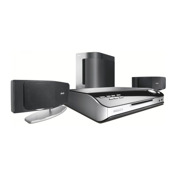
DVD Receiver
CLASS 1
LASER PRODUCT
Contents
1
2
3
4
5
6
Wiring Diagram
7
© Copyright 2006 Philips Consumer Electronics B.V. Eindhoven, The Netherlands.
All rights reserved. No part of this publication may be reproduced, stored in
a retrieval system or transmitted, in any form or by any means, electronic,
mechanical, photocopying, or otherwise without the prior permission of Philips.
Published by KC-TE 0626 AV Systems
Version 1.0
Page
Contents
2
4
8
9
11
14
17
17
18
18
19
20
21
22
8
23
24
25
26
27
28
Printed in the Netherlands
Subject to modification
HTS6510
/
05/12
Page
29
30
31
32
32
32
33
33
33
34
35
36
37
38
38
39
41
41
42
EN 3139 785 32230
Advertisement
Table of Contents

Related Manuals for Philips HTS6510


Summary of Contents for Philips HTS6510
-
Page 1: Table Of Contents
Layout: PCBA 9.1 (Top view) Layout: PCBA 9.1 (Bottom view) © Copyright 2006 Philips Consumer Electronics B.V. Eindhoven, The Netherlands. All rights reserved. No part of this publication may be reproduced, stored in a retrieval system or transmitted, in any form or by any means, electronic, mechanical, photocopying, or otherwise without the prior permission of Philips. -
Page 2: Technical Specifications And Connection Facilities
EN 2 3139 785 32230 Technical Specifi cations and Connection Facilities LOCATION OF PC BOARDS VERSION VARIA TIONS: Type /Versions: HTS6510/05/12 Features & Video (Yellow, Cinch) Component Video, (Y/Pb/Pr) -P-scan SCART (CVBS/RGB) Digital In - Coaxial TV In (Left/Right) Auxiliary (Left/Right) - Page 3 Technical Specifi cations and Connection Facilities 3139 785 32230 EN 3 1. Specifi cations General: COMPACT DISC/VCD/DVD: Mains voltage : 230V Video Decoding : MPEG-1/MPEG-2/ Mains frequency : 50Hz DivX 3/4/5/6, Ultra Power consumption : < 80W at 1/8 P Video DAC : 12 Bits rated...
-
Page 4: Measurements Setup, Service Aid & Lead Free Requirements
EN 4 3139 785 32230 Measurements Setup, Service Aid & Lead Free Requirements 2. Measurements Setup, Service Aid & Lead Free Requirements MEASUREMENT SETUP Tuner FM Bandpass LF Voltmeter 250Hz-15kHz e.g. PM2534 e.g. 7122 707 48001 RF Generator e.g. PM5326 S/N and distortion meter e.g. - Page 5 Measurements Setup, Service Aid & Lead Free Requirements 3139 785 32230 EN 5 SERVICE AIDS Service Tools: Universal Torx driver holder ........4822 395 91019 Torx bit T10 150mm ..........4822 395 50456 Torx driver set T6 - T20 ......... 4822 395 50145 Torx driver T10 extended ........
- Page 6 EN 6 3139 785 32230 Measurements Setup, Service Aid & Lead Free Requirements WAARSCHUWING WARNING Alle IC’s en vele andere halfgeleiders zijn All ICs and many other semi-conductors are gevoelig voor electrostatische ontladingen (ESD). susceptible to electrostatic discharges (ESD). Onzorgvuldig behandelen tijdens reparatie kan Careless handling during repair can reduce life de levensduur drastisch doen verminderen.
- Page 7 Due to lead-free technology some rules have to be respected by the workshop during a repair: • Use only lead-free solder alloy Philips SAC305 with order code 0622 149 00106. If lead-free solder-paste is required, please contact the manufacturer of your solder-equipment.
-
Page 8: 2.2 Service Hints
EN 8 3139 785 32230 Measurements Setup, Service Aid & Lead Free Requirements 2.2 Service Hints CAUTION CHARGED CAPACITORS ON THE SERVO BOARD MAY DAMAGE THE DRIVE ELECTRONICS WHEN CONNECTING A NEW DRIVE.THAT’S WHY, BESIDES THE SAFETY MEASURES LIKE • SWITCH OFF POWER SUPPLY •... -
Page 9: Directions For Use
3. Directions For Use The following except of the Quick Use Guide serves as an introduction to the set. The Complete Direction for the Use can be downloaded in different languages from the internet site of Philips Customer care Center: www.p4c.philips.com... - Page 10 EN 10 3139 785 32230 Directions for Use...
-
Page 11: Dismantling Instructions & Service Positions
Dismantling Instructions & Service Positions 3139 785 32230 EN 11 Dismantling Instructions Dismantling of the Tray Cover Dismantling of the Front Assy, Amplifi er Board & DVD Loader. 1) Loosen 5 screws and remove Panel Left (P129) & Panel Right (Pos 130) by sliding the panels forward as shown in 1) Release 4 snap hooks to remove the Front Board. - Page 12 EN 12 3139 785 32230 Dismantling Instructions & Service Positions 4) Loosen 4 screws (See Figure 4-5) to remove the DVD 6) Loosen 4 screws (See Figure 4-7) to remove PSU Loader. Module. Figure 4 5 Figure 4-7 5) Loosen 4 screws (See Figure 4-6) to remove Amplifi er Board.
- Page 13 Dismantling Instructions & Service Positions 3139 785 32230 EN 13 Dismantling of the PCBAS 9.1 Board, Tuner Service Position Module & AV Board. 1) Loosen 2 screws (See Figure 4-8 & Figure 4-9) to remove the Frame PSU (Pos 162). Insulation Sheet Figure 4-8...
-
Page 14: Service Test Program
EN 14 3139 785 32230 Service Test Program Service Test Program To start service test program refers to Service Mode open the tray with remote control refers to Version or front panel key, while plugging xx refers to Software version number of BEA in the mains cord press 2, 5 8 on (counting up from 01 to 99) remote control, the tray will close... - Page 15 Service Test Program 3139 785 32230 EN 15 5.1.1 Reprogramming of DVD version Matrix 5.1.4 Procedure to upgrade the fi rmware After repair, the customer setting and region code may be lost. 1. Power up the set and open tray. Reprogramming will put the set back in the state in which it has left 2.
- Page 16 EN 16 3139 785 32230 Service Test Program Notes:...
-
Page 17: Block Diagram And Wiring Diagram
Block Diagram, Wiring Diagram 3139 785 32230 EN 17 Wiring Diagram 1601 NC/RDS NC/RDS TU_R TU_R TU_Stereo TU_Stereo TU_L TU_L TU_SD TU_SD TU_SDA TU_SDA TU_SCL TU_SCL Port_S Port_S 1501 1105 1506 1503 1508 HTS6500 Wiring Diagram.pdf 2006-03-13... -
Page 18: Circuit Diagram And Pwb Layout
Circuit Diagram and PWB Layout 3139 785 32230 EN 18 AV Board: Circuit Diagram (Part 1) 1100 B1 F101 A2 1102 F1 F102 A2 1104 D1 F103 A2 1105 H12 F105 A2 1106 E1 F106 B2 2100 C2 F107 B2 2105 D4 F108 B2 3141 4K7... -
Page 19: Av Board: Circuit Diagram (Part 2)
Circuit Diagram and PWB Layout 3139 785 32230 EN 19 AV Board: Circuit Diagram (Part 2) U2 H6 4213 H2 1200 C5 4215 E4 1201 E1 4216 E4 3V3D 1202 G1 4218 D4 1203 G2 4219 E4 5203 2214 1204 +3V3 1204 A6 5104 A4... -
Page 20: Av Board: Circuit Diagram (Part 3)
Circuit Diagram and PWB Layout 3139 785 32230 EN 20 AV Board: Circuit Diagram (Part 3) 1300-1 A11 5306 H11 1301-A E12 6324 A12 1301-B F11 6325 B12 1301-C F11 6326 B12 1302 F1 6327 B12 2300 G4 6328 B12 2301 G4 6329 C11 For Scart version only... -
Page 21: Av Board: Circuit Diagram (Part 4)
Circuit Diagram and PWB Layout 3139 785 32230 EN 21 AV Board: Circuit Diagram (Part 4) 1402 E1 1403 H2 1404 H3 1405 F3 1407 D4 1408 D9 2400 C5 2401 D4 2402 D10 2404 D8 PO_Mute PD_Mute BAS316 4409 4410 2414 A8 +5VD... -
Page 22: Layout: Av Board (Topview)
Circuit Diagram and PWB Layout 3139 785 32230 EN 22 Layout: AV Board (Topview) AVBd_Topview_33616.pdf_2006-04-25... -
Page 23: Layout: Av Board (Bottom View)
Circuit Diagram and PWB Layout 3139 785 32230 EN 23 Layout: AV Board (Bottom view) AVBd_Bottomview_33616.pdf_2006-04-25... -
Page 24: Pcba 9.1: Circuit Diagram (Part 1)
Circuit Diagram and PWB Layout 3139 785 32230 EN 24 PCBA 9.1: Circuit Diagram (Part 1) 1101 D1 3111 A12 6105 H6 1102 F1 3112 A9 6106 I12 1103 H1 3113 A12 7104 D4 1104 I10 3115 A12 7105 D3 CENTRE_CH DV33 1105 F5... -
Page 25: Pcba 9.1: Circuit Diagram (Part 2)
Circuit Diagram and PWB Layout 3139 785 32230 EN 25 PCBA 9.1: Circuit Diagram (Part 2) 1201 D6 F215 D5 3231 G10 1202 D5 3232 H9 F216 D5 1203 A12 3233 G2 F217 D5 1204 A11 3234 H11 F218 D5 1205 A8 3235 G2 F219 D5... -
Page 26: Pcba 9.1: Circuit Diagram (Part 3)
Circuit Diagram and PWB Layout 3139 785 32230 EN 26 PCBA 9.1: Circuit Diagram (Part 3) 1301 D9 1302 F8 2301 C5 2312 A10 2313 C6 DV33 2314 C7 2315 A9 2333 5303 2320 B7 2312 2321 D2 7303-1 100n 74LVC08APW 2322 E6 100n... -
Page 27: Layout: Pcba 9.1 (Topview)
Circuit Diagram and PWB Layout 3139 785 32230 EN 27 Layout: PCBA 9.1 (Topview) PCBA91_Topview_33576.pdf_2006-04-25... -
Page 28: Layout: Pcba 9.1 (Bottom View)
Circuit Diagram and PWB Layout 3139 785 32230 EN 28 Layout: PCBA 9.1 (Bottom view) PCBA91_Bottomview_33576.pdf_2006-04-25... -
Page 29: Fb Control Board: Circuit Diagram
Circuit Diagram and PWB Layout 3139 785 32230 EN 29 FB Control Board: Circuit Diagram 1501 D1 7800 A7 1502 B9 7801 B5 1503 B1 7802 B7 1504 E2 7803 B4 1514 G7 7804 C4 1515 G5 7805 E6 1516 G7 7806 D4 1517 H7 7807 D10... -
Page 30: Layout: Fb Control Board (Top View)
Circuit Diagram and PWB Layout 3139 785 32230 EN 30 Layout: FB Control Board (Top view) FBControlBd_Topview_34094.pdf_2006-04-25... -
Page 31: Layout: Fb Control Board (Bottom View)
Circuit Diagram and PWB Layout 3139 785 32230 EN 31 Layout: FB Control Board (Bottom view) FBControlBd_Bottomview_34094.pdf_2006-04-25... -
Page 32: Fb Display Board: Circuit Diagram
Circuit Diagram and PWB Layout 3139 785 32230 EN 32 FB Display Board: Circuit Diagram Layout: FB Display Board(Top view) 1505 C2 3702 B3 F703 C1 F707 C2 F711 C2 F715 C2 F721 C2 F725 C3 1513 A1 3703 B3 F704 C1 F708 C2 F712 C2... -
Page 33: Fb Volume: Circuit Diagram
Circuit Diagram and PWB Layout 3139 785 32230 EN 33 FB Volume: Circuit Diagram Layout: FB Volume(Top view) 1506 B3 1511 C3 1540 E3 3501 A2 3503 D2 6501 E2 F520 B3 F522 B3 F524 B3 F526 C3 1510 B1 1512 C1 3500 A2 3502 D1... -
Page 34: Hdd Usb: Circuit Diagram
Circuit Diagram and PWB Layout 3139 785 32230 EN 34 HDD USB: Circuit Diagram 1507 D2 1508 D1 1509 D5 1510 D4 1521 B2 1522 D6 1530 E5 4550 1531 D5 2550 A5 2551 B6 UGND 2552 B5 2553 B4 4555 2554 B4 2555 B6... -
Page 35: Layout: Hdd Usb(Top View)
Circuit Diagram and PWB Layout 3139 785 32230 EN 35 Layout: HDD USB (Top view) HDD_USB_Topview_34064.pdf_2006-04-25... -
Page 36: Layout: Hdd Usb(Bottom View)
Circuit Diagram and PWB Layout 3139 785 32230 EN 36 Layout: HDD USB (Bottom view) HDD_USB_Bottomview_34064.pdf_2006-04-25... -
Page 37: Volume Usb: Circuit Diagram
Circuit Diagram and PWB Layout 3139 785 32230 EN 37 Volume USB: Circuit Diagram 1501 D13 7506 B13 1502 F2 7508 E6 1504 E1 7509 E10 1507 H6 7510 I2 1508 H6 7511 I12 1509 H7 7512 I12 1510 H7 7513 I13 1511 H7 F702 E2... -
Page 38: Layout: Volume Usb(Top View)
Circuit Diagram and PWB Layout 3139 785 32230 EN 38 Layout: Volume USB (Top view) Panel_Vol_USB_Topview_34054.pdf_2006-04-25 Layout: Volume USB (Bottom view) Panel_Vol_USB_Bottomview_34054.pdf_2006-04-25... -
Page 39: For Information Only: Psu Module
Circuit Diagram and PWB Layout 3139 785 32230 EN 39 For Information Only: PSU Module PSU06P15-srv1919ww-Circuit.pdf 2006-04-25... - Page 40 Circuit Diagram and PWB Layout 3139 785 32230 EN 40 Notes:...
-
Page 41: Exploded View & Spare Parts List
Exploded View & Spare Parts List 3139 785 32230 EN 41 Exploded View of the Set Figure 8-1... -
Page 42: Spare Parts List
1040 3139 247 12241 MODULE AMP-05-02B 500W (SONO) 1061 3139 248 87902 PCBAS AV BOARD EUROPE HTS6500 1070 3139 248 88211 PCBAS FB VOL-USB BD HTS6510 1111 3139 248 88161 PCBAS FB CONTROL BD HTS6500 1121 3139 248 87832 PCBAS FB DISPLAY HTS4550 1130 3139 248 87491 PCBAS 9.1 HTS6500...
Need help?
Do you have a question about the HTS6510 and is the answer not in the manual?
Questions and answers