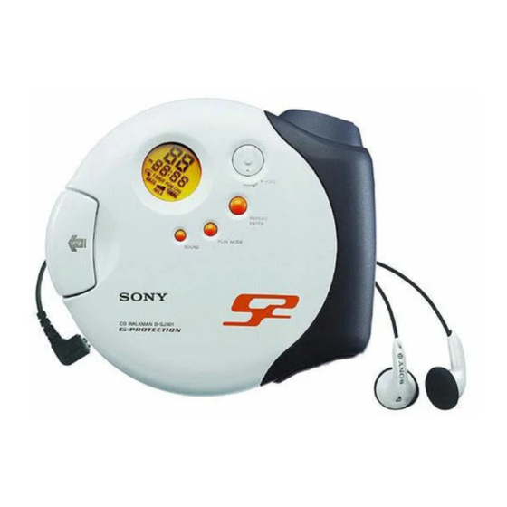
Sony D-SJ301 Service Manual
Hide thumbs
Also See for D-SJ301:
- Operating instructions manual (24 pages) ,
- Specification (2 pages) ,
- Operating instructions manual (25 pages)
Table of Contents
Advertisement
Quick Links
SERVICE MANUAL
Ver 1.2 2004. 04
System
Compact disc digital audio system
Laser diode properties
Material: GaAlAs
Wavelength : λ = 780 nm
Emission duration : Continuous
Laser output : Less than 44.6 µW
(This output is the value measured at a distance
of 200 mm from the objective lens surface on
the optical pick-up block with 7 mm aperture.)
D-A conversion
1-bit quartz time-axis control
Frequency response
+0
40 - 20 000 Hz
dB (measured by JEITA CP-307)
-4.5
Output (at 4.5 V input level)
Headphones (stereo minijack)
Approx. 5 mW + Approx. 5 mW at 16 Ω
Power requirements
For the area code of the model you purchased,
check the upper left side of the bar code on the
package.
• Sony NH-WM2AA rechargeable batteries:
2.4 V DC
• Two LR6 (size AA) batteries: 3 V DC
• AC power adaptor (DC IN 4.5 V jack):
US, CND model:120 V, 60 Hz
AEP, FR, E model: 220 - 230 V, 50/60 Hz
UK model: 230-240V, 50Hz
AUS model: 240 V, 50 Hz
Sony Corporation
9-873-647-03
Personal Audio Company
2004D02-1
Published by Sony Engineering Corporation
© 2004.04
SPECIFICATIONS
Battery life* (approx. hours)
(When you use the CD player on a flat and stable sur-
face.)
Playing time varies depending on how the CD player is
used.
When using
G-PROTECTION function
1
NH-WM2AA
30
(charged for
about 5 hours**)
Two Sony alkaline
47
batteries LR6(SG)
(produced in Japan)
* Measured value by the standard of JEITA (Japan
Electronics and Information Technology
Industries Association).
** Charging time varies depending on how the
rechargeable battery is used.
Operating temperature
5°C - 35°C (41°F - 95°F)
Dimensions (w/h/d) (excluding projecting
parts and controls)
Approx. 133.9 × 38.1 × 147.5 mm
× 1
× 5
3
1
7
(5
⁄
⁄
⁄
in.)
8
2
8
Mass (excluding accessories)
Approx. 305 g (10.8 oz.)
Design and specifications are subject to change
without notice.
D-SJ301
Canadian Model
Australian Model
Model Name Using Similar Mechanism D-E350
CD Mechanism Type
Optical Pick-up Type
Accessories
Supplied accessories
For the area code of the location in which you
purchased the CD player, check the upper left
side of the bar code on the package.
AC power adaptor (1)
2
Headphones (1)
32
Hand strap (1)
50
• Abbreviation
CND : Canadian
AUS : Australian
FR
: French
PORTABLE CD PLAYER
US Model
AEP Model
UK Model
E Model
CDM-3125ER
DAX-25E
Advertisement
Table of Contents

Subscribe to Our Youtube Channel
Related Manuals for Sony D-SJ301


Summary of Contents for Sony D-SJ301
-
Page 1: Specifications
Operating temperature • Sony NH-WM2AA rechargeable batteries: 5°C - 35°C (41°F - 95°F) 2.4 V DC Dimensions (w/h/d) (excluding projecting • Two LR6 (size AA) batteries: 3 V DC parts and controls) Approx. -
Page 2: Table Of Contents
LES COMPOSANTS IDENTIFIÉS PAR UNE MARQUE 0 SUR LES DIAGRAMMES SCHÉMATIQUES ET LA LISTE DES PIÈCES SONT CRITIQUES POUR LA SÉCURITÉ DE FONCTIONNEMENT. NE REMPLACER CES COMPOSANTS QUE PAR DES PIÈCES SONY DONT LES NUMÉROS SONT DONNÉS DANS CE MANUEL OU DANS LES SUPPLÉMENTS PUBLIÉS PAR SONY. -
Page 3: Servicing Notes
D-SJ301 SECTION 1 SERVICING NOTES Laser Diode Checking Methods NOTES ON HANDLING THE OPTICAL PICK-UP BLOCK OR During normal operation of the equipment, emission of the laser diode BASE UNIT is prohibited unless the upper panel is closed while turning ON the S801 (push switch type). -
Page 4: Disassembly
D-SJ301 SECTION 3 DISASSEMBLY The equipment can be removed using the following procedure. MD ASSY “Moter ASSY, turn table (spindle) (M901)” “Lid, Upper”, “Moter ASSY (Sled) (M902)”, Optical pick-up (DAX-25E), Cabinet (front) Main board Note : Follow the disassembly procedure in the numerical order given. -
Page 5: Motor Assy, Turn Table (Spindle) (M901)
D-SJ301 3-3. “MOTOR ASSY, TURN TABLE (SPINDLE) (M901)” 1 Three screws (B1.7x5) Motor ASSY, Turn table (Spindle) (M901) Chassis 3-4. “MOTOR ASSY (SLED) (M902)”, OPTICAL PICK-UP (DAX-25E) 1 Screw (B 1.7x5) Cover, Gear Gear B Screw ASSY, Feed Motor ASSY (Sled) (M902) 4 Screw (P 1.4x3.5) -
Page 6: Electrical Adjustmens
D-SJ301 SECTION 4 ELECTRICAL ADJUSTMENTS The CD section adjustments are done automatically in this set. Focus bias Check Condition: Precautions for Check • Hold the set in horizontal state. 1. Perform check in the order given. 2. Use YEDS-18 disc (Part No.: 3-702-101-01) unless otherwise Connection: indicated. -
Page 7: Diagrams
D-SJ301 SECTION 5 DIAGRAMS 5-1. EXPLANATION OF IC TERMINALS IC601 CXD3029R (SYSTEM CONTROL) Pin No. Pin name Description XRAM DRAM low address strobe signal outut. DRAM data input enable signal output. 3 to 6 D0 to 3 DRAM data bus 0-3. - Page 8 D-SJ301 Pin No. Pin name Description VREFR VREF terminal(R-CH). AOUT2 Audio out (R-CH). – Power supply terminal for DAC block. TEST1 Not used (Fixed at “L”). TEST Not used (Fixed at “L”).. Vss1 – Not used (Fixed at “L”). LRMU OR output of L-CH/R-CH detection flag (AND output) and system flag.
- Page 9 D-SJ301 Pin No. Pin name Description – Power supply terminal for digital. LRCK LR clock output for D/A interface. LRCKI LR clock input for D/A interface. PCMD Serial data output for D/A interface. PCMDI Serial data input for D/A interface.
- Page 10 D-SJ301 Pin No. Pin name Description TSB_I/O – Not used (OPEN). VDD2 – Power supply terminal. EXTBATT_I External battery monitor (Fixed at “H”). TEXTSKIP_I CD text fuction input. “H”: OFF DIGI_TU_I Not used (Fixd to “L”). LODING_I Not used (Fixd to “L”).
-
Page 11: Block Diagram
D-SJ301 5-2. BLOCK DIAGRAM IC602 RAM(16M) D0-3 A0-10 IC601 2,3,24,25 8-12,15-19,21 5 23 4 RF AMP,DIGITAL SERVO DIGITAL SIGNAL PROCESSOR D-RAM CONTROLLER D/A CONVERTER IC301 OPTICAL HEADPHONE AMP PICK-UP BLOCK 4,3,6,5 113-117,11-13,15-17 1 9 2 (DAX-25E) AOUT1 LOUT VCC1_2.0V RFAC... -
Page 12: Printed Wiring Boards -Main Section (1/2)
D-SJ301 Ver 1.1 2002.04 5-3. PRINTED WIRING BOARDS −MAIN SECTION (1/2) − Semiconductor Location MAIN BOARD (SIDE B) Ref. No. Location D102 D202 D302 D401 D404 D406 D407 D461 D602 D805 D809 IC301 IC401 IC402 IC404 IC601 IC602 IC801 Q403... -
Page 13: Printed Wiring Boards -Main Section (2/2)
D-SJ301 5-4. PRINTED WIRING BOARDS −MAIN SECTION (2/2) − • Semiconductor MAIN BOARD (SIDE A) Location Ref. No. Location D408 D804 SWITCH UNIT/LCD D806 D808 IC403 Q404 N > Q408 Q412 > OPTICAL PICK-UP BLOCK DAX–25E M902 SLED MOTOR Note: •... -
Page 14: Schematic Diagram -Main Section (1/3)
D-SJ301 Ver 1.1 2002.04 5-5. SCHEMATIC DIAGRAM – MAIN SECTION (1/3) – • Refer to page 17 for Notes. MAIN BOARD (2/3) (Page 15) MAIN BOARD (2/3) (Page 15) (3/3) (Page 16) MAIN BOARD (2/3) (Page 15) -
Page 15: Schematic Diagram -Main Section (2/3)
D-SJ301 5-6. SCHEMATIC DIAGRAM – MAIN SECTION (2/3) – • Refer to page 17 for Notes. MAIN BOARD (3/3) MAIN BOARD (1/3) (Page 16) (Page 14) MAIN BOARD (1/3) (Page 14) (3/3) (Page 16) MAIN BOARD (1/3) (Page 14) -
Page 16: Schematic Diagram -Main Section (3/3)
D-SJ301 Ver 1.1 2002.04 5-7. SCHEMATIC DIAGRAM – MAIN SECTION (3/3) – • Refer to page 17 for Notes. MAIN BOARD MAIN BOARD (1/3) (Page 14) (2/3) (Page 15) (2/3) (Page 15) -
Page 17: Ic Block Diagram
D-SJ301 Ver 1.1 2002.04 Waveforms Note: • All capacitors are in µF unless otherwise noted. pF: µµF 50 WV or less are not indicated except for electrolytics and tantalums. • All resistors are in Ω and W or less unless otherwise specifed. -
Page 18: Exploded Views
D-SJ301 SECTION 6 Ver 1.1 2002.04 EXPLODED VIEWS NOTE : • -XX, -X mean standardized parts, so they • The mechanical parts with no reference The components identified by mark 0 may have some difference from the original number in the exploded views are not or dotted line with mark 0 are critical one. -
Page 19: Cabinet Section
D-SJ301 Ver 1.2 6-2. CABINET SECTION CDM-3125ER not supplied Ref. No. Part No. Description Remark Ref. No. Part No. Description Remark 3-238-001-01 LID, BATTERY 3-238-002-01 STRAP, BRACKET 3-237-999-01 CABINET (FRONT) 4-908-792-31 SCREW (B2X4) 3-238-014-01 ARM (B) 3-238-007-01 KNOB (VOL) 3-221-329-01 RING, O 3-238-023-01 BUTTON (JOG) 3-338-687-21 SCREW (M1.4X2), TAPPING... -
Page 20: Optical Pick-Up Section (Cdm-3125Er)
D-SJ301 6-3. OPTICAL PICK-UP SECTION (CDM-3125ER) M901 M902 The components identified by Les composants identifiés par une mark 0 or dotted line with mark marque 0 sont critiques pour 0 are critical for safety. la sécurité. Replace only with part number Ne les remplacer que par une pièce... -
Page 21: Electrical Parts List
D-SJ301 Ver 1.1 2002.04 SECTION 7 MAIN ELECTRICAL PARTS LIST NOTE : • Due to standardization, replacements in the • SEMICONDUCTORS In each case, u : µ , for example : The components identified by mark 0 parts list may be different from the parts uA.. - Page 22 D-SJ301 Ver 1.1 2002.04 MAIN Ref. No. Part No. Description Remark Ref. No. Part No. Description Remark C627 1-164-505-11 CERAMIC CHIP 2.2uF IC401 6-702-261-01 IC TB2130AF C628 1-164-505-11 CERAMIC CHIP 2.2uF IC402 8-759-594-55 IC TC75S57F(TE85R) C629 1-162-966-11 CERAMIC CHIP 0.0022uF 10%...
- Page 23 D-SJ301 Ver 1.1 2002.04 MAIN SWITCH Ref. No. Part No. Description Remark Ref. No. Part No. Description Remark R214 1-216-833-11 METAL CHIP 1/16W R636 1-216-845-11 METAL CHIP 100K 1/16W R215 1-216-864-11 METAL CHIP 1/16W R637 1-216-837-11 METAL CHIP 1/16W R352...
- Page 24 D-SJ301 Ver 1.1 2002.04 MAIN SWITCH Ref. No. Part No. Description Remark <SWITCH> S901 1-771-053-21 SWITCH, KEY BOARD (REPEAT/ENTER) S902 1-771-053-21 SWITCH, KEY BOARD (PLAY MODE) S903 1-771-053-21 SWITCH, KEY BOARD (SOUND) S904 1-762-078-11 SWITCH, SLIDE (HOLD) ************************************************************ MISCELLANEOUS **************...
- Page 25 D-SJ301 MEMO...
- Page 26 D-SJ301 REVISION HISTORY Clicking the version allows you to jump to the revised page. Also, clicking the version at the upper right on the revised page allows you to jump to the next revised page. Ver. Date Description of Revision 2002.03...
Need help?
Do you have a question about the D-SJ301 and is the answer not in the manual?
Questions and answers