Table of Contents
Advertisement
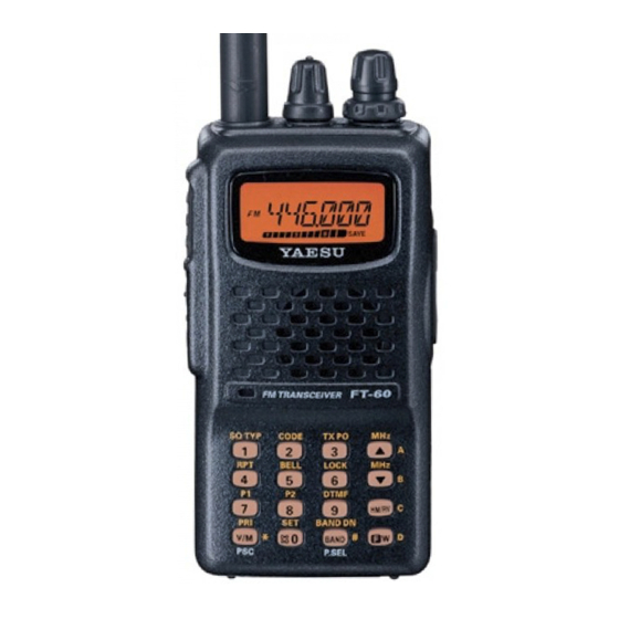
FT-60R
Technical Supplement
©
2005 VERTEX STANDARD CO., LTD.
Specifications ....................................................................................................................................................................2
Exploded View & Miscellaneous Parts .......................................................................................................................4
Block Diagram ..................................................................................................................................................................5
Circuit Description .......................................................................................................................................................... 7
Alignment ..........................................................................................................................................................................9
Board Units (Schematics, Layouts & Parts)
MAIN Unit ................................................................................................................................................................ 13
VR Unit ...................................................................................................................................................................... 47
EH017M90B
Introduction
This manual provides the technical information necessary for
servicing the FT-60R VHF/UHF Dual Band Transceiver.
Servicing this equipment requires expertise in handing sur-
face-mount chip components. Attempts by non-qualified per-
sons to service this equipment may result in permanent dam-
age not covered by the warranty, and may be illegal in some
countries.
Two PCB layout diagrams are provided for each double-sided
board in this transceiver. Each side of the board is referred to
by the type of the majority of components installed on that
side ("Side A" or "Side B"). In most cases one side has only
chip components (surface-mount devices), and the other has
either a mixture of both chip and leaded components (trim-
mers, coils, electrolytic capacitors, ICs, etc.), or leaded compo-
nents only.
While we believe the information in this manual to be correct,
VERTEX STANDARD assumes no liability for damage that
may occur as a result of typographical or other errors that may
be present. Your cooperation in pointing out any inconsisten-
cies in the technical information would be appreciated.
VERTEX STANDARD CO., LTD.
4-8-8 Nakameguro, Meguro-Ku, Tokyo 153-8644, Japan
VERTEX STANDARD
US Headquarters
10900 Walker Street, Cypress, CA 90630, U.S.A.
International Division
8350 N.W. 52nd Terrace, Suite 201, Miami, FL 33166, U.S.A.
YAESU EUROPE B.V.
P.O. Box 75525, 1118 ZN Schiphol, The Netherlands
YAESU UK LTD.
Unit 12, Sun Valley Business Park, Winnall Close
Winchester, Hampshire, SO23 0LB, U.K.
VERTEX STANDARD HK LTD.
Unit 5, 20/F., Seaview Centre, 139-141 Hoi Bun Road,
Kwun Tong, Kowloon, Hong Kong
1
Advertisement
Table of Contents

Related Manuals for Yaesu FT-60R


Summary of Contents for Yaesu FT-60R
- Page 1 Kwun Tong, Kowloon, Hong Kong Introduction This manual provides the technical information necessary for servicing the FT-60R VHF/UHF Dual Band Transceiver. Servicing this equipment requires expertise in handing sur- face-mount chip components. Attempts by non-qualified per- sons to service this equipment may result in permanent dam- age not covered by the warranty, and may be illegal in some countries.
-
Page 2: Specifications
Specifications General Frequency Ranges: 108 - 137 MHz (Air Band), (Cellular Blocked) 137 - 520 MHz (AM/FM), 700 - 999.990 MHz (FM) 144-148 MHz, 430-450 MHz Channel Steps: 5/10/12.5/15/20/25/50/100 kHz Frequency Stability: ±5 ppm @ 14 °F to 140 °F (–10 °C to +60 °C) Repeater Shift: ±600 kHz (144 MHz), ±1.6/5.0/7.6 MHz (430 MHz) Emission Type:... -
Page 3: Exploded View & Miscellaneous Parts
Exploded View & Miscellaneous Parts RA0611600 WINDOW RA0321900 RUBBER CAP RA0599500 FRONT CASE ASSY RA0111400 (W/ MIC SHEET, RING NUT (x2 pcs) PACKING PAD(YER), SP NET,LIGHT GUIDE, DOUBLE FACE(WINDOW)) RA0210600 RUBBER PACKING (x2 pcs) RA0209900 KNOB RA0322000 RUBBER RA0209800 KNOB CP7968001 RA0209700 PANEL ASSY... - Page 4 Exploded View & Miscellaneous Parts Note...
- Page 5 Block Diagram...
- Page 6 Block Diagram...
-
Page 7: Circuit Description
Circuit Description VHF Reception and associated circuitry, and high-pass filter consisting of Q1007 (NJM12902V) and associated circuitry. The filtered Incoming VHF signal is passed through the low-pass fil- audio signal is applied to the audio volume, then passes ter network, antenna switching diode D1066 (HVC131) through the AF ampplifire Q1008 (TDA7233D) and MIC/ and D1068 (RLS135), and low-pass filter network to the SP jack to the internal speaker or an external speaker. -
Page 8: Tx Apc Circuit
Circuit Description The 5 Watts RF signal passes through high-pass filter and high-pass filter network, antenna switch D1044 (RLS135), A portion of the output from the VCO Q1065 (UHF: and another low-pass filter network, and then deliver to 2SC5006) and Q1067 (VHF: 2SC5006), passes through the ANT jack. -
Page 9: Required Test Equipment
Alignment Introduction Required Test Equipment The FT-60R is carefully aligned at the factory for the spec- The following test equipment (and familiarity with its use) ified performance across the amateur band. Realignment is necessary for complete realignment. Correction of prob-... -
Page 10: Entering The Alignment Mode
Entering the Alignment Mode Front-end has a broad bandwidth. Therefore, prior to Alignment of the FT-60R is performed using a front pan- adjustment you must adjust the DIAL knob to set the el software-based procedure. To perform alignment of the frequency to the middle of the band, in step 2, so you transceiver, it must first be placed in the “Alignment... -
Page 11: Tx Power Output
Alignment TX Power Output TX Deviation 1. Tune the frequency to 440.050 MHz, then set the trans- 1. Tune the frequency to 440.050 MHz, then set the trans- mit power level to “LOW.” mit power level to “LOW.” 2. Press the [ F/W ] key, then press the [ BAND ( BAND DN )] 2. -
Page 12: Ctcss Tx Deviation
Alignment 15. Tune the frequency to 146.050 MHz. CTCSS TX Deviation 16. Inject a 146.050 MHz signal at a level of –5 dBµV (with 1. Tune the frequency to 440.050 MHz, then activate the 1 kHz modulation @±3.5 kHz deviation) from the RF CTCSS encoder with a “100 Hz”... - Page 13 MAIN Unit (Lot. 1 ~ 5) Circuit Diagram 440M RX: 1.24 V 146M TX: 8.55 V 440M TX: 0.93 V 440M TX: 8.60 V 850M RX: 0.88 V TX: 1.64 V TX: 1.64 V TX: 0.74 V 146M TX: 1.19 V 440M TX: 1.72 V TX: 2.21 V 146M: +12.4 dBm...
- Page 14 MAIN Unit (Lot. 1 ~ 5) Note...
- Page 15 MAIN Unit (Lot. 1 ~ 5) Parts Layout (Side A) HD64F2266 (Q1031) BU2090FS (Q1055) RD07MVS1 (Q1075) 2SA1774 (FR) 2SC4617 (BR) 3SK296ZQ (ZQ) DTA144EE (16) DTC144EE (26) NJU7007F2 S-80848CNNB UMA8N (A8) DA221 (K) DAN222 (N) DAP222 (P) (Q1051, 1056, 1057, (Q1015, 1017, (Q1081, 1083) (Q1032, 1052, 1061) (Q1014, 1064,...
- Page 16 MAIN Unit (Lot. 1 ~ 5) Parts Layout (Side B) AT24C256N NJM12902V BU2090FS 2SA1774 (FR) 2SC4617 (BR) 2SD1664 (DA) 2SK2596 (BX) DTA144EE (16) DTC144EE (26) NJU7231F30 DA221 (K) (Q1034) (Q1007, 1019, 1020) (Q1030) (Q1038) (Q1003, 1004, 1006, (Q1025) (Q1074) (Q1018, 1027, 1043) (Q1005, 1010, 1021, (Q1001) (D1008, 1020)
- Page 17 MAIN Unit (Lot. 6 ~ 9) Circuit Diagram...
- Page 18 MAIN Unit (Lot. 6 ~ 9) Note...
- Page 19 MAIN Unit (Lot. 6 ~ 9) Parts Layout (Side A) HD64F2266 (Q1031) BU2090FS (Q1055) RD07MVS1 (Q1075) 2SA1774 (FR) 2SC4617 (BR) 3SK296ZQ (ZQ) DTA144EE (16) DTC144EE (26) NJU7007F2 S-80848CNNB UMA8N (A8) DA221 (K) DAN222 (N) DAP222 (P) (Q1051, 1056, 1057, (Q1015, 1017, (Q1081, 1083) (Q1032, 1052, 1061) (Q1014, 1064,...
- Page 20 MAIN Unit (Lot. 6 ~ 9) Parts Layout (Side B) AT24C256N NJM12902V BU2090FS 2SA1774 (FR) 2SC4617 (BR) 2SD1664 (DA) 2SK2596 (BX) DTA144EE (16) DTC144EE (26) NJU7231F30 DA221 (K) (Q1034) (Q1007, 1019, 1020) (Q1030) (Q1038) (Q1003, 1004, 1006, (Q1025) (Q1074) (Q1018, 1027, 1043) (Q1005, 1010, 1021, (Q1001) (D1008, 1020)
- Page 21 MAIN Unit (Lot. 10 ~ 11) Circuit Diagram...
- Page 22 MAIN Unit (Lot. 10 ~ 11) Note...
- Page 23 MAIN Unit (Lot. 10 ~ 11) Parts Layout (Side A) HD64F2266 (Q1031) BU2090FS (Q1055) RD07MVS1 (Q1075) 2SA1774 (FR) 2SC4617 (BR) 3SK296ZQ (ZQ) DTA144EE (16) DTC144EE (26) NJU7007F2 S-80848CNNB UMA8N (A8) DA221 (K) DAN222 (N) DAP222 (P) (Q1051, 1056, 1057, (Q1015, 1017, (Q1081, 1083) (Q1032, 1052, 1061) (Q1014, 1064,...
- Page 24 MAIN Unit (Lot. 10 ~ 11) Parts Layout (Side B) AT24C256N NJM12902V BU2090FS 2SA1774 (FR) 2SC4617 (BR) 2SD1664 (DA) 2SK2596 (BX) DTA144EE (16) DTC144EE (26) NJU7231F30 DA221 (K) (Q1034) (Q1007, 1019, 1020) (Q1030) (Q1038) (Q1003, 1004, 1006, (Q1025) (Q1074) (Q1018, 1027, 1043) (Q1005, 1010, 1021, (Q1001) (D1008, 1020)
- Page 25 MAIN Unit (Lot. 12 ~) Circuit Diagram...
- Page 26 MAIN Unit (Lot. 12 ~) Note...
- Page 27 MAIN Unit (Lot. 12 ~) Parts Layout (Side A) HD64F2266 (Q1031) BU2090FS (Q1055) RD07MVS1 (Q1075) 2SA1774 (FR) 2SC4617 (BR) 3SK296ZQ (ZQ) DTA144EE (16) DTC144EE (26) NJU7007F2 S-80848CNNB UMA8N (A8) DA221 (K) DAN222 (N) DAP222 (P) (Q1051, 1056, 1057, (Q1015, 1017, (Q1081, 1083) (Q1032, 1052, 1061) (Q1014, 1064,...
- Page 28 MAIN Unit (Lot. 12 ~) Parts Layout (Side B) AT24C256N NJM12902V BU2090FS 2SA1774 (FR) 2SC4617 (BR) 2SD1664 (DA) 2SK2596 (BX) DTA144EE (16) DTC144EE (26) NJU7231F30 DA221 (K) (Q1034) (Q1007, 1019, 1020) (Q1030) (Q1038) (Q1003, 1004, 1006, (Q1025) (Q1074) (Q1018, 1027, 1043) (Q1005, 1010, 1021, (Q1001) (D1008, 1020)
-
Page 29: Main Unit
MAIN Unit Parts List DESCRIPTION VALUE TOL. MFR'S DESIG VXSTD P/N VERS. SIDE LAY ADR PCB with Components (W/ VR Unit) CP7965002 USA A2U PCB with Components (W/ VR Unit) CP7965003 EXP A1 PCB with Components (W/ VR Unit) CP7965004 EXP A2 PCB with Components (W/ VR Unit) CP7965005... - Page 30 MAIN Unit Parts List DESCRIPTION VALUE TOL. MFR'S DESIG VXSTD P/N VERS. SIDE LAY ADR C 1055 CHIP CAP. 6.3V GRM188B10J105KA01D K22084801 C 1056 CHIP CAP. 0.0068uF GRM36B682K25PT K22148803 C 1056 CHIP CAP. 0.0068uF GRM36B682K25PT K22148803 AUSTRALIA 3 C 1056 CHIP CAP.
- Page 31 MAIN Unit Parts List DESCRIPTION VALUE TOL. MFR'S DESIG VXSTD P/N VERS. SIDE LAY ADR C 1129 CHIP CAP. 100pF GRM1552C1H101JD01D K22178236 C 1130 CHIP CAP. 12pF GRM1552C1H120JZ01D K22178214 C 1131 CHIP CAP. 0.001uF GRM155B11H102KA01D K22178809 C 1132 CHIP CAP. 6.3V GRM188B10J105KA01D K22084801...
- Page 32 MAIN Unit Parts List DESCRIPTION VALUE TOL. MFR'S DESIG VXSTD P/N VERS. SIDE LAY ADR C 1202 CHIP CAP. 10pF GRM36CH100B50PT K22178297 C 1203 CHIP CAP. 0.001uF GRM155B11H102KA01D K22178809 C 1204 CHIP CAP. 0.001uF GRM155B11H102KA01D K22178809 C 1206 CHIP CAP. 0.001uF GRM155B11H102KA01D K22178809...
- Page 33 MAIN Unit Parts List DESCRIPTION VALUE TOL. MFR'S DESIG VXSTD P/N VERS. SIDE LAY ADR C 1280 CHIP CAP. GRM1554C1H2R0BZ01D K22178289 C 1281 CHIP CAP. GRM1553C1H3R0BZ01D K22178290 C 1282 CHIP CAP. 0.001uF GRM155B11H102KA01D K22178809 C 1283 CHIP CAP. GRM1552C1H8R0BZ01D K22178295 C 1284 CHIP CAP.
- Page 34 MAIN Unit Parts List DESCRIPTION VALUE TOL. MFR'S DESIG VXSTD P/N VERS. SIDE LAY ADR C 1350 CHIP CAP. 0.001uF GRM155B11H102KA01D K22178809 C 1351 CHIP CAP. 0.001uF GRM155B11H102KA01D K22178809 C 1352 CHIP CAP. 0.001uF GRM155B11H102KA01D K22178809 C 1353 CHIP CAP. GRM1554C1H1R0BZ01D K22178287 C 1354...
- Page 35 MAIN Unit Parts List DESCRIPTION VALUE TOL. MFR'S DESIG VXSTD P/N VERS. SIDE LAY ADR D 1007 DIODE DAN222 TL G2070174 D 1008 DIODE DA221 TL G2070178 D 1009 DIODE M1FM3-4063 G2070804 D 1010 DIODE 1SS400 TE61 G2070634 D 1011 DIODE RB551V-30 TE-17 G2070892...
- Page 36 MAIN Unit Parts List DESCRIPTION VALUE TOL. MFR'S DESIG VXSTD P/N VERS. SIDE LAY ADR D 1080 SURGE ABSORBER TVSF0805 Q9000807 D 1082 DIODE HSC277TRF G2070584 DS1001 LCD A15A013X G6090160 HS1001 HEATSINK PLATE RA0455500 J 1001 SHIELD FINGER 4025 3100089 S5000225 J 1002 SHIELD FINGER...
- Page 37 MAIN Unit Parts List DESCRIPTION VALUE TOL. MFR'S DESIG VXSTD P/N VERS. SIDE LAY ADR L 1060 M.RFC 0.082uH C1608CB-82NG L1691044 L 1061 M.RFC 0.082uH C1608CB-82NG L1691044 L 1062 M.RFC 0.082uH C1608CB-82NG L1691044 L 1063 M.RFC LK1608 1R0K-T L1690687 L 1064 M.RFC 0.047uH TFL0816-47...
- Page 38 MAIN Unit Parts List DESCRIPTION VALUE TOL. MFR'S DESIG VXSTD P/N VERS. SIDE LAY ADR Q 1051 TRANSISTOR 2SA1774 TL R G3117748R Q 1052 TRANSISTOR DTA144EE TL G3070074 Q 1053 TRANSISTOR 2SC4617 TL R G3346178R Q 1054 TA75S01F TE85R G1091593 Q 1055 BU2090FS-E1 G1092187...
- Page 39 MAIN Unit Parts List DESCRIPTION VALUE TOL. MFR'S DESIG VXSTD P/N VERS. SIDE LAY ADR R 1034 CHIP RES. 1/16W RMC1/16S 223JTH J24189041 R 1035 CHIP RES. 1/16W RMC1/16S 333JTH J24189043 R 1036 CHIP RES. 1/16W RMC1/16S 563JTH J24189046 R 1037 CHIP RES.
- Page 40 MAIN Unit Parts List DESCRIPTION VALUE TOL. MFR'S DESIG VXSTD P/N VERS. SIDE LAY ADR R 1096 CHIP RES. 1/16W RMC1/16S 223JTH J24189041 R 1097 CHIP RES. 1/16W RMC1/16S 101JTH J24189013 R 1098 CHIP RES. 1/16W 0.5% RR0510P-103-D J24189143 R 1099 CHIP RES.
- Page 41 MAIN Unit Parts List DESCRIPTION VALUE TOL. MFR'S DESIG VXSTD P/N VERS. SIDE LAY ADR R 1164 CHIP RES. 1/16W RMC1/16S JPTH J24189070 VER. A3 R 1164 CHIP RES. 1/16W RMC1/16S JPTH J24189070 VER. C1 R 1164 CHIP RES. 1/16W RMC1/16S JPTH J24189070 VER.
- Page 42 MAIN Unit Parts List DESCRIPTION VALUE TOL. MFR'S DESIG VXSTD P/N VERS. SIDE LAY ADR R 1216 CHIP RES. 2.2k 1/16W RMC1/16S 222JTH J24189029 R 1217 CHIP RES. 1/16W RMC1/16S 683JTH J24189047 R 1218 CHIP RES. 820k 1/16W RMC1/16S 824JTH J24189060 R 1219 CHIP RES.
- Page 43 MAIN Unit Parts List DESCRIPTION VALUE TOL. MFR'S DESIG VXSTD P/N VERS. SIDE LAY ADR R 1290 CHIP RES. 1/16W RMC1/16S 103JTH J24189037 R 1291 CHIP RES. 2.2k 1/16W RMC1/16S 222JTH J24189029 R 1292 CHIP RES. 2.2k 1/16W RMC1/16S 222JTH J24189029 R 1293 CHIP RES.
- Page 44 MAIN Unit Parts List DESCRIPTION VALUE TOL. MFR'S DESIG VXSTD P/N VERS. SIDE LAY ADR R 1363 CHIP RES. 1/16W RMC1/16S 331JTH J24189019 R 1364 CHIP RES. 1/16W RMC1/16S 102JTH J24189025 R 1365 CHIP RES. 470k 1/16W RMC1/16S 474JTH J24189057 R 1366 CHIP RES.
-
Page 45: Parts List
MAIN Unit Parts List DESCRIPTION VALUE TOL. MFR'S DESIG VXSTD P/N VERS. SIDE LAY ADR S 1004 TACT SWITCH EVQP4403M N5090132 TH1001 THERMISTOR TBPS1R473K475H5Q G9090068 TH1002 THERMISTOR TBPS1R103K440H5Q G9090067 TH1003 THERMISTOR TBPS1R104K475H5Q G9090069 X 1001 XTAL TRS-4.0 4MHz 4.000MHZ H0103283 X 1001 XTL XJNGGIDANF 4MHz... - Page 46 MAIN Unit Parts List Parts List DESCRIPTION VALUE TOL. MFR'S DESIG VXSTD P/N VERS. SIDE LAY ADR...
- Page 47 VR Unit Circuit Diagram 13.2 V 13.5 V 11.4 V 11.5 V 2.96 V 1.42 V 2.33 V 0.81 V...
-
Page 48: Parts Layout
VR Unit Parts Layout (Side A) (Side B) 2SC4617 (BR) BRPY1211F (Q2001, 2002) (D2001) Parts List DESCRIPTION VALUE TOL. MFR'S DESIG VXSTD P/N VERS. LOT SIDE LAY ADR Printed Circuit Board AH017M000 FR0118000 C 2001 CHIP CAP. 0.0047uF GRM36B472K25PT K22148830 C 2002 CHIP CAP. - Page 50 Copyright 2005 VERTEX STANDARD CO., LTD. All rights reserved No portion of this manual may be reproduced without the permission of VERTEX STANDARD CO., LTD.
Need help?
Do you have a question about the FT-60R and is the answer not in the manual?
Questions and answers