Table of Contents
Advertisement
Quick Links
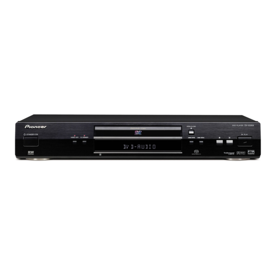
DVD PLAYER
DV-656A-S
DV-656A-K
THIS MANUAL IS APPLICABLE TO THE FOLLOWING MODEL(S) AND TYPE(S).
Model
DV-656A-S
WYXJ
DV-656A-K
WYXJ
For details, refer to "Important symbols for good services".
PIONEER CORPORATION
PIONEER ELECTRONICS (USA) INC. P.O. Box 1760, Long Beach, CA 90801-1760, U.S.A.
PIONEER EUROPE NV Haven 1087, Keetberglaan 1, 9120 Melsele, Belgium
PIONEER ELECTRONICS ASIACENTRE PTE. LTD. 253 Alexandra Road, #04-01, Singapore 159936
PIONEER CORPORATION 2002
Type
Power Requirement
AC220-240V
AC220-240V
4-1, Meguro 1-chome, Meguro-ku, Tokyo 153-8654, Japan
DV-656A-S
Reginal restriction
codes (Region No.)
2
2
T-ZZE JULY 2002 printed in Japan
ORDER NO.
RRV2649
Remarks
Advertisement
Table of Contents

Related Manuals for Pioneer DV-656A-S


Summary of Contents for Pioneer DV-656A-S
-
Page 1: Dvd Player
PIONEER CORPORATION 4-1, Meguro 1-chome, Meguro-ku, Tokyo 153-8654, Japan PIONEER ELECTRONICS (USA) INC. P.O. Box 1760, Long Beach, CA 90801-1760, U.S.A. PIONEER EUROPE NV Haven 1087, Keetberglaan 1, 9120 Melsele, Belgium PIONEER ELECTRONICS ASIACENTRE PTE. LTD. 253 Alexandra Road, #04-01, Singapore 159936... -
Page 2: Safty Information
PLAY signal, or when the PLAY key is pressed (S104 ON in the FLKY assy), with the above requirements satisfied. 2. When the cover is open, close viewing through the objective lens with the naked eye will cause exposure to the laser beam. ∗ : See page 61. DV-656A-S... - Page 3 By following the instructions in this manual, be sure to apply the prescribed grease or glue to proper portions by the appropriate amount.For replacement parts or tools, the prescribed ones should be used. DV-656A-S...
-
Page 4: Table Of Contents
7.1.6 ERROR DISPLAY ..........................72 7.1.7 TEST POINTS LOCATION & WAVEFORMS ..................75 7.1.8 TROUBLE SHOOTING ......................... 77 7.1.9 DISASSEMBLY ............................. 79 7.2 IC ................................85 7.3 DISC / CONTENT FORMAT PLAYBACK COMPATIBILITY ..............119 7.4 CLEANING............................. 120 8. PANEL FACILITIES ............................121 DV-656A-S... -
Page 5: Specifications
SRS Labs, Inc. Accessories • Stereo Audio Cable (VDE1052) • Power Cable (ADG1154) • AA/R6P Dry Cell Batteries (L = 1.5m) White • Video Cable (VDE1053) • Remote Control (VXX2800) (L = 1.5m) Yellow DV-656A-S... -
Page 6: Exploded Views And Parts List
For the applying amount of lubricants or glue, follow the instructions in this manual. (In the case of no amount instructions, apply as you think it appropriate.) 2.1 PACKING 15–17 "Operating Instructions" FRONT DV-656A-S... - Page 7 ARY7022 Operating Instructions VRD1162 Polyethylene Bag VHL1051 (Italian / Dutch) Pad L VHA1307 (2) CONTRAST TABLE DV-656A-S/WYXJ and DV-656A-K/WYXJ are constructed the same except for the following: DV-656A-S/ DV-656A-K/ Mark No. Symbol and Description WYXJ WYXJ 13 Packing Case VHG2223...
-
Page 8: Exterior Section
2.2 EXTERIOR SECTION NON-CONTACT SIDE CONTACT SIDE Refer to "2.4 LOADING MECHA ASSY". Refer to "2.3 FRONT PANEL SECTION". DV-656A-S... - Page 9 VRW1889 PCB Holder VEC2283 PCB Holder VEC2283 NSP 23 Base Chassis VNA2521 (2) CONTRAST TABLE DV-656A-S/WYXJ and DV-656A-K/WYXJ are constructed the same except for the following: DV-656A-S/ DV-656A-K/ Mark No. Symbol and Description WYXJ WYXJ 24 Rear Panel VNA2462 VNA2487...
-
Page 10: Front Panel Section
2.3 FRONT PANEL SECTION • Tray Panel Section NON-CONTACT SIDE CONTACT SIDE DV-656A-S... - Page 11 Pioneer Badge See Contrast table (2) Screw BBZ30P100FZK • • • • • • • • • • (2) CONTRAST TABLE DV-656A-S/WYXJ and DV-656A-K/WYXJ are constructed the same except for the following: DV-656A-S/ DV-656A-K/ Mark No. Symbol and Description WYXJ WYXJ...
-
Page 12: Loading Mecha Assy
Carriage DC Motor / 0.3W PXM1027 Screw JGZ17P028FMC Flexible Cable (26P) VDA1864 Screw Z39-019 Connector Assy 2P VKP2253 Tray VNL1920 Float Rubber VEB1327 Belt VEB1330 Stabilizer VNE2253 Loading Base VNL1917 Float Base DVD VNL1918 Drive Cam VNL1919 Gear Pulley VNL1921 Loading Gear VNL1922 DV-656A-S... - Page 13 GYA1001 Daifree No. 23 Daifree No. 23 GEM1036 Tray GEM1036 Tray Concave of unevenness Concave of unevenness Inner side of a ditch Daifree GEM1036 Bottom View Top View Side of the rib Concave of unevenness Daifree Daifree GEM1036 GEM1036 DV-656A-S...
-
Page 14: Traverse Mechanism Assy-S
GEM1037 Silicone Adhesive GEM1037 4 (Adjustment Screw) 17 (Torque : 0.12 ± 0.01 N•m) DVDM CN111 Screw Tight Silicone Adhesive GYL1001 GEM1037 To DVDM 17 (Torque : 0.12 ± 0.01 N•m) CN115 To DVDM CN114 NON-CONTACT SIDE CONTACT SIDE DV-656A-S... - Page 15 Guide Bar VLL1514 Sub Guide Bar VLL1515 Hold Spring VNC1017 Joint Spring VNC1019 Support Spring VNC1020 NSP 11 Mechanism Chassis VNE2248 Slider VNL1811 Spacer VNL1913 Joint VNL1914 FFC Holder VNL1915 Screw BBZ20P050FZK Tapping Screw OBA8009 Screw PMA26P100FMC Damper Sheet VEB1335 DV-656A-S...
-
Page 16: Block Diagram And Schematic Diagram
3.3V IC481 LOD POS CN602 SM8707HV (2P) SW1(GNDS) Clock Generator S101 CN402 (17P) Remote V101 Sensor VAW1073 Unit FL TUBE KEYB ASSY SEL IR FLKY ASSY IR101 IC101 PE5314B KEY0 FL Control KEY1 CN201 CN102 CN101 (4P) (4P) (17P) DV-656A-S... - Page 17 AUDIO_L AUDIO_L L IN IC901 MM1505XN RY903 V/Y OUT V IN IC902 MM1507XN AV CONNECTOR CN901 JA902 (RGB) - TV (19P) L OUT L IN IC903 MM1507XN B IN G IN RY904 R/C IN V OUT RY905 V IN DV-656A-S...
-
Page 18: Power Supply Block
V+3D UNIT CN101 CN401 (13P) (13P) V+12 V33EV V+3E V+12 EV6V (B) EV6V (A) -28V -28V IC101 FLDC+ FLDC+ FLDC- FLDC- LIVE SW+12V CN402 CN101 EV+4V AC IN V101 (17P) (17P) FL TUBE SW+3.3 NEUTRAL DVDM ASSY FLKY ASSY DV-656A-S... - Page 19 DV-656A-S...
-
Page 20: Loab Assy And Overall Wiring Diagram
3.2 LOAB ASSY and OVERALL WIRING DIAGRAM SACDB ASSY (VWG2378) JACB ASSY (VWV1914) SCRB ASSY Note : When ordering service parts, be sure (VWV1922) to refer to "EXPLODED VIEWS and PARTS LIST" or "PCB PARTS LIST". DV-656A-S... - Page 21 KEYB ASSY (VWG2366) FLKY ASSY (VWG2355) POWER SUPPLY UNIT (VWR1352) DVDM ASSY (VWS1539) SPINDLE MOTOR : VXX1088 STEPPING MOTOR : VXM1090 LOADING MOTOR ASSY LOAB ASSY : VXX2505 (VWG2346) DV-656A-S...
-
Page 22: Dvdm Assy 1/4 [Fts Block]
: FOCUS SERVO LOOP LINE Buffer (RF) : TRACKING SERVO LOOP LINE : STEPPING SERVO LOOP LINE Buffer (RF) (RF_V) (RF_A) (RF) Buffer (RF) (RF) LD Driver for DVD SW for LD Driver Defect Signal for CD (RF) CN601 (F) (F) DV-656A-S... - Page 23 (RF_V) VCO Circuit (RF_V) RF Amp. (RF for SACD Water Mark detection) : The power supply is shown with the marked box. (RF_A) DV-656A-S...
-
Page 24: Dvdm Assy 2/4 [Fr Block]
3.4 DVDM ASSY 2/4 [FR BLOCK] DVDM ASSY (VWS1539) PGM 16M FLASH MEMORY FR CPU DV-656A-S... - Page 25 Clock Signals: Refer to "7.1.7 TEST POINT LOCATION & WAVEFORMS" 3.3V Regulator CN901 DV-656A-S...
-
Page 26: Dvdm Assy 3/4 [Eby/Av1 Block]
3.5 DVDM ASSY 3/4 [EBY/AV1 BLOCK] DVDM ASSY (VWS1539) (AD) (AD) DVD data Decoder (RF_V) (RF_V) DV-656A-S... - Page 27 : The power supply is shown with the marked box. MPEG, DVD-Audio, DTS Decoder Progressive scan Processer (RF_V) : RF (VIDEO) SIGNAL ROUTE (VD) : VIDEO DATA SIGNAL ROUTE (AD) : AUDIO DATA SIGNAL ROUTE : AUDIO (DIGITAL) SIGNAL ROUTE DV-656A-S...
-
Page 28: Dvdm Assy 4/4 [Venc Block]
3.6 DVDM ASSY 4/4 [VENC BLOCK] (VD) DVDM ASSY (VWS1539) (Y/G) (Pb/B) (Pr/R) DV-656A-S... - Page 29 : C SIGNAL ROUTE : B SIGNAL ROUTE (Pb) : Pb SIGNAL ROUTE : AUDIO (DIGITAL) SIGNAL ROUTE DATA2A DATA1A DATA2 DATA1 CN101 Buffer CN701 (Pr/R) Buffer (Pb/B) (Y/G) 16 19 Buffer 15 18 Buffer (Y/G) Buffer (Pr/R) Buffer (Pb/B) DV-656A-S...
-
Page 30: Jacb Assy 1/2 [Audio Block]
Audio DAC for Front channel (2 ch) 21 22 24 23 +8V Regulator +5V Regulator DIGITAL AUDIO OUT COAXIAL CN551 DIGITAL AUDIO OUT OPTICAL Audio DAC for Ls, Rs (2 ch) Audio DAC for C, LFE (Sub Woofer) (2 ch) DV-656A-S... - Page 31 (with LPF) Ls ch. for Mute Control Rs ch. Signal Center LFE ch. (Sub Woofer) Audio out Audio Amp. : The power supply is shown with the marked box. (with LPF) for Mute Control Signal LPF: Low Pass Filter DV-656A-S...
-
Page 32: Jacb Assy 2/2 [Video Block]
: Y SIGNAL ROUTE : C SIGNAL ROUTE (Pb) : Pb SIGNAL ROUTE (Pr) : Pr SIGNAL ROUTE : R SIGNAL ROUTE : G SIGNAL ROUTE : B SIGNAL ROUTE : AUDIO (DIGITAL) SIGNAL ROUTE : AUDIO SIGNAL ROUTE DV-656A-S... - Page 33 : The power supply is shown with the marked box. Composite Video out (Y/G) (Pb/B) (Pr/R) Video out (Pb) (Pr) Component Video out CN901 DV-656A-S...
-
Page 34: Sacdb Assy
3.9 SACDB ASSY SACDB ASSY (VWG2378) (AD) (AD) CN531 (AD) (AD) DV-656A-S... - Page 35 : The power supply is shown with the marked box. (AD) : AUDIO DATA SIGNAL ROUTE : AUDIO (DIGITAL) SIGNAL ROUTE (AD) CN102 DV-656A-S...
-
Page 36: Flky And Keyb Assys
3.10 FLKY and KEYB ASSYS FLKY ASSY (VWG2355) DV-656A-S... - Page 37 FLKY ASSY KEYB ASSY S101 : 0 (OPEN/CLOSE) S201 : FL DIMMER S102 : 7 (STOP) S202 : VIDEO OFF S103 : 8 (PAUSE) S203 : POWER STANDBY/ON S104 : 3 (PLAY) S105 : ¡ ¢ S106 : 4 1 DV-656A-S...
-
Page 38: Scrb Assy
3.11 SCRB ASSY SCRB ASSY (VWV1922) Buffer Buffer CN702 (R/C) Video Amp. with SW Video Amp. with SW (Y/V) (Y/V) Video Amp. DV-656A-S... - Page 39 : R SIGNAL ROUTE : AUDIO SIGNAL ROUTE : G SIGNAL ROUTE : B SIGNAL ROUTE RY901-RY905: Relay SW (R/C) (Y/V) (R/C) (R/C) (R/C) (R/C) (R/C) (Y/V) (Y/V) (Y/V) (Y/V) : The power supply is shown with the marked box. DV-656A-S...
-
Page 40: Power Supply Unit
3.12 POWER SUPPLY UNIT DV-656A-S... -
Page 41: Waveforms [Dvdm Assy]
Foot of R957 (Pr) V: 0.5V/div. H: 0.2µsec/div. V: 1V/div. H: 5msec/div. V: 0.2V/div. H: 10µsec/div. IC201 - pin 1 (EFM) Foot of R964 (V) Foot of R959 (Y) Progressive V: 1V/div. H: 0.2µsec/div. V: 0.2V/div. H: 10µsec/div. V: 0.2V/div. H: 10µsec/div. DV-656A-S... -
Page 42: Waveforms [Jacb Assy]
: DVD-REF-A1, T2-Chap.1 IC301-pin 4 (LRCK) V: 1V/div. H: 5µsec/div. IC301-pin 5 (DATA0) V: 1V/div. H: 500nsec/div. IC301-pin 6 (BCK) V: 1V/div. H: 100nsec/div. IC301-pin 7 (PMCK) V: 1V/div. H: 20nsec/div. IC302 - pin 1 (Analog OUT) V: 1V/div. H: 500µsec/div. DV-656A-S... -
Page 43: Pcb Connection Diagram
Transistor B C E SIDE A Transistor with resistor B C E Field effect SIDE B Chip Part P.C.Board transistor Resistor array 3-terminal regulator SIDE A SIDE B LOAB ASSY (VNP1836-B) CN602 CN601 CN601 CN602 CN103 LOADING MOTOR ASSY DV-656A-S... -
Page 44: Dvdm Assy
4.2 DVDM ASSY SIDE A DVDM ASSY CN701 CN901 (VNP1886-B) Q931 Q934 Q932 Q933 IC901 IC403 IC831 IC801 IC271 IC281 IC791 Q103 IC481 IC751 IC201 IC302 IC261 IC601 CN901 CN101 CN531 CN402 DV-656A-S... - Page 45 SIDE B DVDM ASSY (VNP1886-B) IC404 IC902 Q938 Q939 Q936 IC931 IC402 Q941 Q937 IC553 Q102 Q940 Q101 IC101 IC786 Q935 IC552 Q106 Q104 IC304 Q241 IC781 IC491 IC351 Q210 IC251 IC211 IC701 Q601 IC603 IC741 DV-656A-S...
-
Page 46: Jacb Assy
4.3 JACB ASSY SIDE A JACB ASSY (VNP1887-C) KN102 CN701 CN901 CN702 CN901 IC702 IC101 IC102 DV-656A-S... - Page 47 SIDE A CN551 CN101 CN102 CN902 DV-656A-S...
- Page 48 Q322 Q361 Q360 Q352 Q351 Q350 Q420 Q520 Q510 Q533 Q531 Q431 Q432 Q320 Q310 Q321 Q362 Q370 Q371 Q410 Q532 Q311 Q312 Q430 Q530 Q534 Q201 IC302 IC304 IC305 IC402 IC503 IC202 IC301 IC303 IC403 IC501 IC201 IC401 DV-656A-S...
- Page 49 SIDE B CN701 CN702 Q701 IC701 DV-656A-S...
-
Page 50: Sacdb Assy
IC906 C943 IC906 C921 C832 R923 IC904 C922 IC804 R922 IC804 C972 C951 C955 C973 C971 C841 C977 C839 CONTACT SIDE CONTACT SIDE CN903 CN801 CONTACT SIDE CN901 CN901 CN531 SACDB ASSY (VNP1885-A) SIDE B SIDE B IC991 CN902 DV-656A-S... -
Page 51: Scrb Assy
R945 C941 D910 C951 R962 C945 D915 R964 D913 R966 C957 D912 R968 C924 R967 D903 C917 C901 R905 R904 R912 R903 R931 C906 Q901 R902 R908 R915 C910 C907 D901 C904 R911 R914 C902 C950 D902 R959 C919 DV-656A-S... -
Page 52: Flky And Keyb Assys
4.6 FLKY and KEYB ASSYS SIDE A KEYB ASSY (VNP1888-A) IC103 W120 L101 V101 SIDE B Q102 Q101 R206 R207 R205 R201 R216 R202 R215 R208 KEYB ASSY (VNP1888-A) DV-656A-S... - Page 53 W144 45A/KU VWG2393 VWG2355 /RAM S101 VWG2394 VWG2356 OPEN PLAY VWG2376 PAUSE 656A/KU STOP S104 S103 W156 W113 FLKY CN101 S102 W112 E M PF2 CN101 CN402 SIDE B IC101 IC102 Q103 Q104 Q105 CN101 CN101 FLKY ASSY (VNP1888-A) DV-656A-S...
-
Page 54: Power Supply Unit
4.7 POWER SUPPLY UNIT SIDE A SIDE A AC IN POWER SUPPLY UNIT Q320 VR201 IC103 IC201 Q412 Q411 Q410 DV-656A-S... -
Page 55: Pcb Parts List
IC402 MM1565AF C411, C413, C414, C419, C422 CEV101M16 IC601 PD6345A C801 CEV101M16 IC701 PE5286A C103 CEV220M16 > IC403 PQ025EZ01ZP C119, C205, C326, C421, C424 CEV221M4 IC481 SM8707HV C470, C472, C601, C623 CEV221M4 IC786 TC74VHC541FT C701, C702, C711, C745 CEV221M4 DV-656A-S... - Page 56 R755 RS1/16S1801F R754 RS1/16S3001F C350, C360, C414, C424 CEAT470M16 R751 RS1/16S3301F C110, C725, C762, C763 CEAT471M6R3 R132 RS1/16S4702F C101, C103, C107, C314, C324 CEJQ101M16 C338, C372, C374, C380, C401 CEJQ101M16 R810, R817 RS1/16S6800F C410, C416, C420, C501, C510 CEJQ101M16 DV-656A-S...
- Page 57 CN701 30P CONNECTOR VKN1261 CN801 7P CONNECTOR VKN1267 SEMICONDUCTORS CN102 19P CONNECTOR VKN1775 D203, D204 SLR-343VC(NPQ) KN101, KN102 EARTH METAL FITTING VNF1084 SWITCHES AND RELAYS SACDB ASSY S201–S203 ASG7013 SEMICONDUCTORS RESISTORS > IC906 BA25BC0FP All Resistors RS1/16S###J IC901 CXD2753R DV-656A-S...
- Page 58 C901, C902, C907, C909 CKSRYF104Z25 C916, C917, C924, C925, C928 CKSRYF104Z25 C935, C936, C938–C941, C945 CKSRYF104Z25 C950, C956–C959 CKSRYF104Z25 RESISTORS R932, R937, R943, R950, R955 RS1/16S75R0F R965 RS1/16S75R0F Other Resistors RS1/16S###J OTHERS JA901, JA902 CONNECTOR VKB1157 CN901 19P CONNECTOR VKN1279 DV-656A-S...
-
Page 59: Adjustment
Tangential Radial adjustment adjustment screw screw [Electrical Part] Electrical adjustments are not required. 6.2 JIGS AND MEASURING INSTRUMENTS Test mode remote control Screwdriver (large) Screwdriver (medium) TV monitor unit (GGF1067) Screw tight (GYL1001) DVD test disc Precise screwdriver (GGV1025) DV-656A-S... -
Page 60: Necessary Adjustment Points
Purpose: To set the sweep which was correct with the individual Traverse mechanism. Be sure to perform the following step finally when replaced Pickup, Traverse Mechanism and Spindle Motor. CLEAR GGF1067 Test mode remote control unit (It is necessary when performed adjustment procedure Ÿ.) DV-656A-S... -
Page 61: Test Mode
An address is displayed < When playback with the target address of disc (DVD)> For example, when playback with # 30000 During PLAY CHP/TIM Press keys in order 030000 TEST MODE: OFF POWER GGF1067 Test mode remote control unit DV-656A-S... -
Page 62: Mechanism Adjustment
Mechanism Base and turn each screw to adjust the height. (Refer to "6.1 ADJUSTMENT ITEMS AND LOCATION".) Spacer for Height adjustment Note: Turn the Short switch to Short side when Turn a flat side removing the Pickup Flexible Cable. into bottom (Refer to "7.1.9 DISASSEBLY".) DV-656A-S... - Page 63 J4 : Min If error rate is OK, Disc playback normally. • The measurement of block error rate locks a root of tangential and radial adjustment screws with the Screw tight, and go to step Screw tight: GYL1001 Test mode end DV-656A-S...
- Page 64 Initialize the Focus Sweep Setting Purpose: To set the sweep which was correct with the individual Traverse mechanism. Turn on the Player POWER CLEAR Note: Be sure to perform this step when replaced the Pickup or Traverse mechanism. DV-656A-S...
-
Page 65: General Information
[Player's ID Data Setting] number. [Player's ID Number Setting] ID Number ? > 0 0 0 0 0 0 0 0 1 OK ? <PLAY> Compare Mode <SEARCH> Enter Loading The ID Data Disc ! Input ID Number ! DV-656A-S... - Page 66 Compare Compare > * * * * * * * * * > 0 0 0 0 0 0 0 0 1 OK ? <CLEAR> Exit <PLAY> Enter <STOP> Memory Clear Input ID Number ! Input ID Number ! DV-656A-S...
-
Page 67: Self-Diagnosis Function Of Pickup Defective
Replace the Traverse Mechanism Assy or Pickup. Note : When a DVD disc or a CD disc is played in the test mode, this function is effective. Character in bold : Item name : Information display Laser diode current value DV-656A-S... -
Page 68: Test Mode Screen Display
: [IN ] CD active area : [CD] $ Version of the flash ROM [V: ∗. ∗ ∗ ∗] Flash ROM size [FLSH = ∗] % Revision of the system controller [S: ∗ . ∗ / ∗ ∗ ∗ ] DV-656A-S... - Page 69 2 C1 error value of DVD [ER – ∗ ∗ ∗ ∗ ∗ ∗ ∗ ∗ ] _ Internal operation mode of mechanism controller [MM – ∗ ∗ : ∗ ∗] Internal mechanism mode (2 digits) and internal mechanism step (2 digits) of the mechanism controller DV-656A-S...
-
Page 70: Self-Diagnosis Function
Display the mechanism error history and self diagnosis result by pressing the "CHP / TIM" key once again. Afterwards press the "CHP / TIM" key with toggle and change the display. Display screen of mechanism error history and self diagnosis result DV-656A-S... -
Page 71: Function Specification Of The Service Mode
EDC Error which occurred in the same block in succession. will be increased. As for this, CPU power is used for update of OSD drawing, symptoms occur so that control of VBR Buffer is not in time. Indication contents DV-656A-S... -
Page 72: Error Display
Were not able to playback from the disc distinction process. 38 Disc-type- PLAY or STOP was not completed by backup operation of the disc distinction. Open sensing error Distinguished it from the blank disc in the ATB process completion. DV-656A-S... - Page 73 Subcode check No frame could be read for 3 failure during Stop seconds or more. playback ID can not read An ID could not be read within 1 second after the AFB Opens during startup tracking on. (ID readout failure) DV-656A-S...
- Page 74 10 etc. check sum error AV1 access error No operation or it becomes debugging bit3=1 08 etc. (read, write NG) indication if the power is able to ON. bit2=1 04 etc. LSI11 access error bit0=1 01 etc. SRAM access error DV-656A-S...
-
Page 75: Test Points Location & Waveforms
7.1.7 TEST POINTS LOCATION & WAVEFORMS SIDE A SIDE A DVDM ASSY 16MDSP 16MEBY 22/24M 22/24AV1 27MAV1 27MDSP 33MSACD 33MEBY1 36MEBY FPWM VPWM PPWM RPWM DV-656A-S... - Page 76 V: 500mV/div. H: 2msec/div. AC mode Foot of R264 (RPWM) Foot of R957 (Pr) V: 1V/div. H: 5msec/div. V: 0.2V/div. H: 10µsec/div. Foot of R964 (V) Foot of R959 (Y) Progressive V: 0.2V/div. H: 10µsec/div. V: 0.2V/div. H: 10µsec/div. DV-656A-S...
-
Page 77: Trouble Shooting
DVDM Assy CN105-pin 12 (INSIDE SW signal) • Check the loading drive signal : IC351-pin 14, 15, 16 • Check the +6V and +12V power supply voltage (If above voltage is not supplied, check the micro-fuse P101 and P102.) DV-656A-S... - Page 78 • Check digital data of video and audio signals (audio signals: 3 line data, video signals: or beeing damaged? (noisy) 8bit data) shown to each schematic diagram and an analog signal line. In addition, check CLK. audio system: 22/24MHz, video system: 27MHz Indicate the error message. Refer to the section "7.1.6 ERROR DISPLAY". DV-656A-S...
-
Page 79: Disassembly
Close the Tray (0). → Clamp the Test Disc. Release the PCB Support. Remove the DVDM Assy. Turn power OFF. PCB Support Pull out the Power Cord from the outlet. Cutting Pliers DVDM Assy Test Disc (Flexible Cable) This is not installed in this unit. DV-656A-S... - Page 80 Connect two Extension Cables and a Extension Board as figure below. 17P Extension Cable 21P Extension Cable for Service for Service [GGF1157] [GGD1298] Loading Mecha Assy POWER SUPPLY Unit CN561 CN402 CN101 JACB Assy SACDB Assy (DV-45A Only) DVDM Assy Extension Board for Service [GGF1430] Front Panel Section Diagnosis DV-656A-S...
- Page 81 10 (DSD Rs), pin 12 (DSD Ls), pin 14 (DSD LFE), pin 16 (DSD C). SACDB ASSY SIDE B CN902 pin 2 (SACDSL) pin 4 (DSDBCK) pin 6 (DSD R) pin 16 (DSD C) pin 8 (DSD L) pin 14 (DSD LFE) pin 10 (DSD Rs) pin 12 (DSD Ls) DV-656A-S...
- Page 82 Caution in the Tray Insertion × 4 In the Tray insertion, insert it after matching a triangle mark of the Loading Base and a position of pin of the Drive Cam. Triangle Mark Loading Base Loading Mecha Assy DVDM Assy Drive Cam DV-656A-S...
- Page 83 Screw is locked with Silicone Adhesive. Please lock it with Silicone Adhesive when installs it. Unhook ( × 4) Remove the Traverse Mechanism Assy-S Silicone Adhesive GEM1037 Slider × 2 Hold Spring Pickup Assy-S Joint × 2 Traverse Mechanism Assy-S Silicone Adhesive GEM1037 DV-656A-S...
- Page 84 Move the Pickup to the innermost of the disc Perform the styling as shown in figure below. Lose slack Fold position of step Bottom View Bottom View Fold at the position Reference line of reference line. Bottom View Bottom View DV-656A-S...
- Page 85 • The information shown in the list is basic information and may not correspond exactly to that shown in the schematic diagrams. • List of IC LA9704W, LC78652W, BA6664FM, SM8707HV, PD6345A, M65776AFP, AD7172KST, PCM1738EG-3, DSD1702EG, LA73054, CXD2753R, PE5314B, PE5286A 7 LA9704W (DVDM ASSY : IC101) • RF IC ¶ Block Diagram DV-656A-S...
- Page 86 ¶ Pin Function c i f z i l i f i l l l u l l u DV-656A-S...
- Page 87 – x i f z i l z i l DV-656A-S...
- Page 88 Error Detect VCOC Generator Correction EFLG C1-Twofold, XOUT C2-Fourfold XTALOUT ADRAO LRSY ROMCK Command Supplement/Mute Serial Out ROMXA Interface D Attenuate Deemphasis Filter P0-7 63-70 BUSYB DOUT DOUT LASER FBUSYB 25,27 TEST1-4 38,50 53,54 PP0-3 General Purpose Register RESB DV-656A-S...
- Page 89 ¶ Pin Function t f i − − l l i t t i y t i t l i − − − − a i l t l i − DV-656A-S...
- Page 90 − − l l i l i f − t l i f t l i f t l i f − − − − − l l i − l l i t t i − − DV-656A-S...
- Page 91 Control reference pin of output voltage Output pin Output voltage control pin GND pin Power save pin FG signal output pin Power supply pin Gain switching pin Hall signal input pins Motor power pin Resistor connection pin for output current detection Hall bias pin DV-656A-S...
- Page 92 • Clock Generate IC ¶ Pin Arrangement ¶ Pin Function . r i x i f x i f x i f x i f n i l L " : " " : " l l u x i f – DV-656A-S...
- Page 93 7 PD6345A (DVDM ASSY : IC601) • FR CPU ¶ Pin Function − − − − − − DV-656A-S...
- Page 94 : " c t i i f i l " : " t i s c t i t i s c t i l a i n i l – l a i n i l – − DV-656A-S...
- Page 95 − − c t i − − " " L " ) " l a i l a i l a i − − − − − − − − DV-656A-S...
- Page 96 − − − − x i f − − x i f − − − ← DV-656A-S...
- Page 97 7 M65776AFP (DVDM ASSY : IC751) • MPEG2 Decorder IC ¶ Block Diagram DV-656A-S...
- Page 98 DV-656A-S...
- Page 99 . r i – – " " L – – DV-656A-S...
- Page 100 . r i – – – DV-656A-S...
- Page 101 4:2:2 TO P0-P7 4:4:4 SATURATION CONTROL (COLOR INTER- MODULATOR 10BIT PROGRAMMABLE DAC F MATRIX DATA) POLATOR ADD BURST CHROMA FILTER CONTROL 10BIT INTERPOLATOR DAC D REAL-TIME SIN/COS ESET1 CONTROL CIRCUIT CONTROL DDS SLOCK BLOCK COMP1 12,13,18,26,31,47 SCRESET/RTC ¶ Pin Function DV-656A-S...
- Page 102 - l l i l p " " e t s i i r r t i s l l i i r r v i t . s l " " 1 v i t , y l DV-656A-S...
- Page 103 7 PCM1738EG-3 (JACB ASSY : IC301) • D/A Converter IC ¶ Pin Arrangement ¶ Pin Function DV-656A-S...
- Page 104 7 DSD1702EG (JACB ASSY : IC401, IC501) • D/A Converter IC ¶ Block Diagram ¶ Pin Arrangement ¶ Pin Function DV-656A-S...
- Page 105 7 LA73054 (JACB ASSY : IC701) • DVD Video Amplifier ¶ Block Diagram DV-656A-S...
- Page 106 ¶ Pin Function – – – – c i t s l l . ) t DV-656A-S...
- Page 107 7 CXD2753R (SACDB ASSY : IC901) • SACD Decorder ¶ Pin Arrangement DV-656A-S...
- Page 108 ¶ Pin Function t f i L " . " " " L " " x i f " " L x i f " " L DV-656A-S...
- Page 109 " " x i f " " L x i f " " x i f " " L DV-656A-S...
- Page 110 " " L x i f " " L x i f " " L DV-656A-S...
- Page 111 DV-656A-S...
- Page 112 L " : " c t i l l o " " " / : " " / " L " : " " " L " / : " L " / " L " : " DV-656A-S...
- Page 113 . r i − l l o − − − v i t l l o − l l u t s i l l o DV-656A-S...
- Page 114 − . t i − . t i − . t i − - t l i g i − − - t l . y l . y l l l a z i l . t i DV-656A-S...
- Page 115 . t i . t i . t i . t i v i t . t i . t i s l l v i t t s i . t i . t r z i l DV-656A-S...
- Page 116 . r i . ) ) . t r t l i t DV-656A-S...
- Page 117 . r i y t i . t r . t r y t i l a i v i t DV-656A-S...
- Page 118 . r i t f i n i l g i l - t l - t l - t l - t l , t i . t i DV-656A-S...
-
Page 119: Disc / Content Format Playback Compatibility
7.3 DISC / CONTENT FORMAT PLAYBACK COMPATIBILITY DV-656A-S... -
Page 120: Cleaning
7.4 CLEANING Before shipping out the product, be sure to clean the following positions by using the prescribed cleaning tools: Position to be cleaned Cleaning tools Pickup lenses Cleaning liquid : GEM1004 Cleaning paper : GED-008 DV-656A-S... -
Page 121: Panel Facilities
8. PANEL FACILITIES DV-656A-S... - Page 122 DV-656A-S...
- Page 123 DV-656A-S...
- Page 124 DV-656A-S...
- Page 125 DV-656A-S...
Need help?
Do you have a question about the DV-656A-S and is the answer not in the manual?
Questions and answers