Sony MDS-JA333ES Service Manual
Minidisc deck
Hide thumbs
Also See for MDS-JA333ES:
- Operating instructions manual (112 pages) ,
- Limited warranty (1 page) ,
- Operating instructions manual (112 pages)
Table of Contents
Advertisement
SERVICE MANUAL
U.S. and foreign patents licensed from Dolby Laboratories
Licensing Corporation.
System
Disc
Laser
Laser output
Laser diode
Revolutions (CLV)
Error correction
Sampling frequency
Coding
Modulation system
Number of channels
Frequency response
Signal-to-noise ratio
Wow and flutter
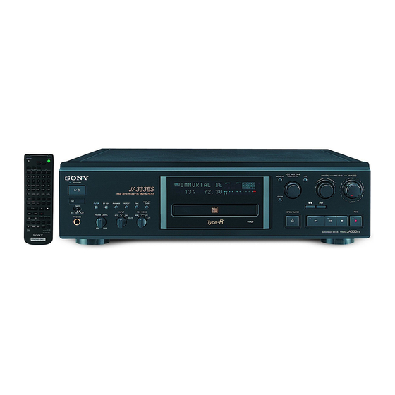
MDS-JA333ES
Photo : GOLD
SPECIFICATIONS
MiniDisc digital audio system
MiniDisc
Semiconductor laser ( λ = 780 nm)
Emission duration: continuous
MAX 44.6 µW
1
)
1) This output is the value
measured at a distance of
200 mm from the objective lens
surface on the Optical Pick-up
Block with 7 mm aperture.
Material: GaAlAs
400 rpm to 900 rpm
ACIRC (Advanced Cross Interleave
Reed Solomon Code)
44.1 kHz
ATRAC (Adaptive TRansform
Acoustic Coding)/ATRAC 3
EFM (Eight-to-Fourteen
Modulation)
2 stereo channels
5 to 20,000 Hz ±0.3 dB
Over 100 dB during play
Below measurable limit
Model Name Using Similar Mechanism
MD Mechanism Type
Base Unit Type
Optical Pick-up Type
Inputs
ANALOG IN
Jack type: phono
Impedance: 47 k Ω
Rated input: 500 mVrms
Minimum input: 125 mVrms
DIGITAL IN OPT1
Connector type: square optical
Impedance: 660 nm (optical wave
length)
DIGITAL IN OPT2
Connector type: square optical
Impedance: 660 nm (optical wave
length)
DIGITAL IN COAXIAL
Jack type: phono
Impedance: 75 Ω
Rated input: 0.5 Vp-p, ±20 %
Outputs
PHONES
Jack type: stereo phone
Rated output: 28 mW
Load impedance: 32 Ω
ANALOG OUT
Jack type: phono
Rated output: 2.5 Vrms (at 50
k Ω)
Load impedance: over 10 k Ω
US Model
Canadian Model
AEP Model
UK Model
MDS-JA555ES
MDM-6J
MBU-5J
KMS-260B/J1N
— Continued on next page —
MINIDISC DECK
Advertisement
Table of Contents

Subscribe to Our Youtube Channel
Related Manuals for Sony MDS-JA333ES


Summary of Contents for Sony MDS-JA333ES
- Page 1 MDS-JA333ES SERVICE MANUAL US Model Canadian Model AEP Model UK Model Photo : GOLD U.S. and foreign patents licensed from Dolby Laboratories Model Name Using Similar Mechanism MDS-JA555ES Licensing Corporation. MD Mechanism Type MDM-6J Base Unit Type MBU-5J Optical Pick-up Type...
- Page 2 DIAGRAMMES SCHÉMATIQUES ET LA LISTE DES PIÈCES SONT CRITIQUES POUR LA SÉCURITÉ DE FONCTIONNEMENT. NE VAROITUS REMPLACER CES COMPOSANTS QUE PAR DES PIÈSES SONY DONT LES NUMÉROS SONT DONNÉS DANS CE MANUEL OU Parist voi räjähtää, jos se on virheellisesti asennettu.
-
Page 3: Table Of Contents
TABLE OF CONTENTS Laser component in this product is capable of emitting radiation exceeding the limit for 1. SERVICING NOTE ·························································· 6 Class 1. 2. GENERAL ········································································ 12 3. DISAssembly 3-1. Case ·················································································· 16 3-2. Loading Panel ··································································· 16 3-3. Front Panel Assembly ······················································· 17 3-4. - Page 4 The deck’s self-diagnosis function automatically checks the condition of the MD deck when an error occurs, then issues a three- or five-digit code and an error message on the display. If the code and message alternate, find them in the following table and perform the indicated countermeasure. Should the problem persist, consult your nearest Sony dealer. Three- or five-...
- Page 5 [ITEMS OF ERROR HISTORY MODE ITEMS AND CONTENTS] Display Details of History op rec tm Displays the total recording time. When the total recording time is one minute or longer, displays the time and minute. When the total recording time is less than one minute, displays “Under 1 min”. The displayed time is about 1/4 of the actual recording time when the laser is set to the high power state.
-
Page 6: Servicing Note
Forced Reset Use this function when the MDS-JA333ES cannot be operated normally due to hung-up of the microprocessor. It is recommended to use this function when you cannot exit the test mode or the retry-cause-display mode, or when the normal operation cannot be performed after the MDS-JA333ES is disassembled once then re-assembled. - Page 7 [BD Board Waveform Check Tool] Use of the exclusive tool (J-2501-149-A) is convenient to check the waveforms on the BD board. GND : Ground terminal I+3V : For measuring IOP (Checking deterioration of the optical pick-up laser) : For measuring IOP (Checking deterioration of the optical pick-up laser) TEO : TRK error signal (traverse adjustment) : Reference level for when checking signals : RF signal (jitter check)
- Page 8 (BD Board IC171)] The IOP data that is indicated on the optical pick-up, can be saved in the non-volatile memory of the MDS-JA333ES. Saving the IOP data in the memory eliminates the needs to look at the printed value on the label that is attached on the surface of optical pick-up, and enables to view the IOP data on display.
- Page 9 Note: The judgment criterion is shown for the purpose of judging if the performance is acceptable or not. This is not the specification value for adjustment. Use the specification value for adjustment when the MDS-JA333ES is going to be adjusted.
- Page 10 8. When you want to enter the “Track mode”, press the N button to start playback. 9. To exit the test mode, press the ?/1 button. The message “TOC” flashes, the MDS-JA333ES enters the standby mode and exits the test mode.
- Page 11 Higher Bits Lower Bits Details Hexa- Hexadecimal decimal When 0 When 1 b7 b6 b5 b4 b3 b2 b1 b0 Binary Emphasis OFF Emphasis ON Monaural Stereo This is 2-bit display. Normally 01. 01:Normal audio. Others:Invalid Audio (Normal) Invalid Original Digital copy Copyright exists No copyright...
-
Page 12: General
SECTION 2 GENERAL This section is extracted from instruction manual. Front panel description 3456 1 ?/1 (power) switch/STANDBY indicator (14) (23) qh OPEN/CLOSE A button (14) (23) Press to turn on the deck. When you turn on the deck, Press to insert or eject the MD. the STANDBY indicator turns off. -
Page 13: Remote Control Description
Remote control description 8 x button (15) (23) Press to stop play or recording, or cancel the selected operation. OPEN/CLOSE 9 X button (14) (23) Press to pause play or recording. Press again to resume MENU/NO play or recording. 0 x button (14) (18) (19) DISPLAY SCROLL TIME... -
Page 14: Display Window Description
Display window description 1 REMOTE indicator 5 INPUT indicators (14) Lights when the MD is being controlled by an external • “OPT1” lights when the program source connected device connected to the deck. to the DIGITAL IN OPT1 connector is selected. 2 Disc name and track name indicators display •... -
Page 15: Setting The Clock
Rear panel description 1 ANALOG IN jacks (11) (14) Use to input analog signals from other components. 2 ANALOG OUT jacks (11) Use to output analog signals to other components. 4 5 6 7 3 DIGITAL IN COAXIAL jack (11) (14) Connect a digital coaxial cable to input digital signals from other components. -
Page 16: Disassembly
SECTION 3 DISASSEMBLY Follow the disassembly procedure in the numerical order given. Note : 3-1. CASE 4 Remove the upper case 3 Two screws in the direction of the arrow A ( TP,FLAT HEAD) 2 Two screws (TP,FLAT HEAD) 1 Two screws (TP,FLAT HEAD) 3-2. -
Page 17: Front Panel Assembly
3-3. FRONT PANEL ASSEMBLY 5 Two screws × 8 6 Two bracket (F) 2 Connector (CN303) 3 Connector (CN651) 1 Flat type wire (CN807) 7 Front panel assembly 4 Six screws × 3-4. MD MECHANISM DECK 1 Two screws × (BVTT3 3 Four screws 2 Two lug... -
Page 18: Tray Assembly
3-5. TRAY ASSEMBLY 6 Bracket (top) 2 Two screws 4 Two screws (BV2.6) (BV2.6) 9 Screw 5 Lug (BV2.6) 0 Stopper (shaft B) 7 Three gears 3 Lug (top) qa Shaft 8 Three gears (top) qs Remove the tray assembly in the direction of the arrow B . -
Page 19: Bu Holder Assembly
3-6. BU HOLDER ASSEMBLY 5 Two scews (BV2.6) 6 Two collars 2 Two scews (damper) (BV2.6) 3 Two collars (damper) 4 Two compression 7 Two compression springs springs 8 BU holder assembly Fig. A Slider 1 Turn the pully gear to align the slider with of the rib. -
Page 20: Base Unit (Mbu-5J)
3-8. BASE UNIT (MBU-5J) 1 Leaf spring (UDL) 2 Leaf spring (UDR) 3 Remove the holder assembly in the direction of the arrow A . 6 Base unit 5 Two screws 4 Two screws (BV2.6) (BV2.6) 3-9. BD BOARD 6 Two precision screws (+P1.7 ×... -
Page 21: Over Light Head (Hr901)
3-10. OVER LIGHT HEAD (HR901) 2 Screw 3 Over light head (P1.7 × 6) (HR901) 1 Flexible board (CN104) 3-11. MINI DISC DEVICE (KMS-260B/J1N) 3 Screw 4 Leaf spring (shaft) (B2 × 8) 5 Main shaft 6 Remove the mini disc device (KMS-260B/J1N) in the direction of the arrow A . -
Page 22: Test Mode
4-1. Precaution on Using the Test Mode • Be sure to insert and eject a disc after confirming that the disc in the MDS-JA333ES has come to complete stop because the loading related movements of the mechanism are performed without any relationship with the test mode. - Page 23 4-5. Selecting the Test Mode There are 26 types of the test mode. The group can be switched by rotating the lAMSL knob. All the adjustments and checks for service can be performed in the test mode of the service group. There is the Develop group, but it is not used for service.
- Page 24 4-5-1. Operating the Continuos Playback Mode 1. Entering the continues playback mode 1) Load the disc into the unit. (recordable disc or disc for playback) The disc is loaded by pushing the tray. 2) Rotate the lAMSL knob to display “CPLAY1MODE” (C34). 3) Press the YES button to change the display to “CPLAY1MID”.
- Page 25 4-5-2. Operating the Continuos Recording Mode (Use this mode for self record/playback check only) 1. Entering the continuos recording mode 1) Load the recordable disc to the unit. The disc is loaded by pushing the tray. 2) Rotate the lAMSL knob to display “CREC 1MODE” (C35). 3) Press the YES button to change the display to “CREC1MID”.
- Page 26 4-7. Test Mode Displays The DISPLAY key is used to switch display modes. The display modes are switched in the following order each time the DISPLAY key is pressed. Order Description Example of display MODE display CPLAY1 ( Error rate display Address display Auto gain display Detrack display...
-
Page 27: Electrical Adjustments
SECTION 5 ELECTRICAL ADJUSTMENTS 5-1. On Part Replacement and Adjustment • Perform the checks and adjustments of the MDM and MBU blocks following the procedure below . The procedure is changed depending on the replaced part. Start • Abbreviation : Optical pick-up OWH : Overwrite head •... - Page 28 5-2. Precautions for Checking Laser Diode 2) Set the test mode when performing the adjustments. After completing the adjustments, exit the test mode. Emission Perform the adjustments and checks in “Group S” of the test To check the emission of the laser diode during adjustments, never mode.
- Page 29 5-5. Creating Continuos Recorded Disc 5-6-2. Laser Power Check Before check: • This disc is used in focus bias adjustment and error rate check. • Refer to Section 1 “Service note” How to open the disc tray when The following describes how to create a continuos recording disc. power switch is turned off, and laser power check.
- Page 30 5-6-3. Traverse Check 8. Observe the waveform of the oscilloscope and confirm it that is within the specified value. Do not rotate the lAMSL Note 1 : If the recorded disc is used for this adjustment, the knob at this time. data is deleted.
- Page 31 • The error rate is checked using the self record/playback disc. Manufacture the self record/playback disc by user locally using Checking procedure: the MDS-JA333ES that is going to be measured of its error rate 1. Load the test disc (MDW-74/GA-1). by means of continuous recording.
- Page 32 The IOP data that is indicated on the pick-up, can be saved in the Adjustment non-volatile memory of the MDS-JA333ES. The IOP data that is The temperature data at 25°C is used as the reference data and is printed on the optical pick-up and the IOP data after adjustment is saved in the non-volatile memory for offset adjustment.
- Page 33 2. Rotate the lAMSL knob to display “LDPWR ADJUS” 5-11. Traverse Adjustment (C04). (laser power: for adjustment) Note1: If the recorded disc is used for this adjustment, the data 3. Press the YES button once to display “LD 0.9mW $ ”.
- Page 34 8. Rotate the lAMSL knob so that the waveform of the 18. Press the YES button to save the adjustment results in the non- oscilloscope is the specified value. (The figure of the “ EFB volatile memory. (At this time “EFB = SAV”...
- Page 35 9. Press the MENU/NO button and press the A button to eject 5-13. Error Rate Check the test disc. 5-13-1. CD Error Rate Check Checking procedure: Note 1 : If the C1 error and ADER are out of the specified value at 1.
- Page 36 5-16. Adjusting Points and Connecting Points [BD BOARD] (SIDE A) CN101 D101 CN110 I+3V NOTE IC171 Note: It is recommended to use the tool for BD board waveform check when the waveform is checked. (Refer to page 7 of Service note.) [BD BOARD] (SIDE B) IC101 IC121...
-
Page 37: Ic Block Diagrams
6-22. IC BLOCK DIAGRAMS IC101 CXA2523AR (BD BOARD) 43 42 USROP – RF AGC – USRC RFA1 BPF3T RFA2 RFA3 PEAK3T – HLPT –1 – – –2 – OFST PTGR TEMP PEAK – –2 – 36 BOTM BOTTOM – –1 GRVA PBSW 35 ABCD... - Page 38 IC121 CXD2662R (BD BOARD) 100 99 98 97 96 95 94 93 92 91 90 89 88 87 86 85 84 83 82 81 80 79 78 77 76 SPINDLE GENERATOR SERVO 75 TE MNT0 74 SE MNT1 EACH MONITOR 73 AVSS BLOCK CONTROL...
- Page 39 IC404,406 SN74HCU04ANS-E05 (DIO BOARD) IC405 SN74HC153ANS-E05 (DIO BOARD) DATA INPUTS STROBE OUTPUT 2C3 2C2 2C1 2C0 SELECT 2C3 2C2 2C1 2C0 1C3 1C2 1C1 1C0 IC651 M5218AP (HP BOARD) STROBE 1C3 1C2 1C1 1C0 OUTPUT SELECT DATA INPUTS OUT1 OUT2 –IN1 +IN1 –IN2...
- Page 40 IC504,505 CXA8042AS (DA BOARD) IC305,306,307,308 NJM2114D (AD BOARD) OUT1 IN2– I01+ I02– IN2+ –IN1 OUT2 I01– IN1+ +IN1 –IN2 SWITCHING I02+ IN1– CIRCUIT VCC2 +IN2 GND2 VEE2 VCC1 CONSTANT REFERENCE VEE1 CURRENT VREF VOLTAGE CIRCUIT CIRCUIT CONTROL VCNT CIRCUIT CIREF GND1 RIREF IC302...
- Page 41 IC250 LB1641 (POW BOARD) T.S.D O.C.P MOTOR MOTOR DRIVE DRIVE FWD/REV/STOP CONTROL LOGIC...
-
Page 42: Diagrams
MDS-JA333ES SECTION 6 DIAGRAMS 6-1. BLOCK DIAGRAMS MAIN SECTION IC402 IC404 IC404 DIGITAL OPT1 INPUT DIGITAL IC401 IN OPT IC405 IC404 IC404 DIGITAL DSSP/DSP OPT2 INPUT IC121 DIN0 J400 HR901 IC404 IC404 OVER WRITE DIGITAL HEAD EFMO IN COAXIAL OVER WRITE... -
Page 43: Display/Power Supply Section
MDS-JA333ES DISPLAY/POWER SUPPLY SECTION P DOWN MAIN SECTION REGULATOR/ DISPLAY CONTROL J461 FL781 RESET GEN IC801(2/2) FL DRIVER IC280 CONTROL FLOURESCENT IC771 A1 II A1 IN INDICATOR TUBE P DOWN P DOWN RESET A1 OUT LF901 Q321 D+5V TR901 PH5V... -
Page 44: Circuit Board Location
MDS-JA333ES 6-2. CIRCUIT BOARD LOCATION THIS NOTE IS COMMON FOR PRINTED WIRING BOARDS AND SCHEMATIC DIAGRAMS. (In addition to this, the necessary note is printed in each block.) AC board POW board Note on Schematic Diagram: Note on Printed Wiring Boards: •... -
Page 45: Printed Wiring Board Bd Section
MDS-JA333ES 6-3. PRINTED WIRING BOARD BD SECTION • Refer to page 39 for Note on Printed Wiring Boards. • Refer to page 39 for Circuit Board Location. (Page 50) (Page 48) • Semiconductor Location Ref. No. Location Ref. No. Location... -
Page 46: Schematic Diagram Bd Section (1/2)
MDS-JA333ES 6-4. SCHEMATIC DIAGRAM BD SECTION (1/2) • Refer to page 39 for Note on Schematic Diagrams. • Refer to page 60 for Waveforms. • Refer to page 61 for IC Block Diagram. • Refer to page 67 for IC Pin Function. -
Page 47: Schematic Diagram Bd Section (2/2)
MDS-JA333ES 6-5. SCHEMATIC DIAGRAM BD SECTION (2/2) • Refer to page 39 for Note on Schematic Diagrams. • Refer to page 60 for Waveforms. • Refer to page 61 for IC Block Diagrams. • Refer to page 66 for IC Pin Function. -
Page 48: Schematic Diagram Bd Switch Section
MDS-JA333ES 6-6. SCHEMATIC DIAGRAM BD SWITCH SECTION • Refer to page 39 for Note on Schematic Diagrams. 6-7. PRINTED WIRING BOARD BD SWITCH SECTION • Refer to page 39 for Note on Printed Wiring Boards. • Refer to page 39 for Circuit Board Location. -
Page 49: Printed Wiring Board Bd Switch Section
MDS-JA333ES 6-8. PRINTED WIRING BOARD AD SECTION • Refer to page 39 for Note on Printed Wiring Boards. • Refer to page 39 for Circuit Board Location. There are few cases that the part printed on this diagram isn’t mounted in this model. -
Page 50: Schematic Diagram Ad Section
MDS-JA333ES 6-9. SCHEMATIC DIAGRAM AD SECTION • Refer to page 39 for Note on Schematic Diagrams. • Refer to page 64 for IC Block Diagrams. -
Page 51: Printed Wiring Board Dio Section
MDS-JA333ES 6-10. PRINTED WIRING BOARD DIO SECTION • Refer to page 39 for Note on Printed Wiring Boards. • Refer to page 39 for Circuit Board Location. There are few cases that the part printed on this diagram isn’t mounted in this model. -
Page 52: Schematic Diagram Dio Section
MDS-JA333ES 6-11. SCHEMATIC DIAGRAM DIO SECTION • Refer to page 39 for Note on Schematic Diagrams. • Refer to page 63 for IC Block Diagrams. -
Page 53: Printed Wiring Board Da Section
MDS-JA333ES 6-12. PRINTED WIRING BOARD DA SECTION • Refer to page 39 for Note on Printed Wiring Boards. • Refer to page 39 for Circuit Board Location. There are few cases that the part printed on this diagram isn’t mounted in this model. -
Page 54: Schematic Diagram Da Section
MDS-JA333ES 6-13. SCHEMATIC DIAGRAM DA SECTION • Refer to page 39 for Note on Schematic Diagrams. • Refer to page 60 for Waveform. -
Page 55: Printed Wiring Board Digital Section
MDS-JA333ES 6-14. PRINTED WIRING BOARD DIGITAL SECTION • Refer to page 39 for Note on Printed Wiring Boards. •Refer to page 39 for Circuit Board Location. There are few cases that the part printed on this diagram isn’t mounted in this model. -
Page 56: Schematic Diagram Digital Section
MDS-JA333ES 6-15. SCHEMATIC DIAGRAM DIGITAL SECTION • Refer to page 39 for Note on Schematic Diagrams. • Refer to page 60 for Waveform. • Refer to page 70 for IC Pin Function. PIN FUNCTION... -
Page 57: Schematic Diagram Hp Section
MDS-JA333ES 6-16. SCHEMATIC DIAGRAM HP SECTION • Refer to page 39 for Note on Schematic Diagrams. • Refer to page 63 for IC Block Diagrams. -
Page 58: Printed Wiring Board Hp Section
MDS-JA333ES 6-17. PRINTED WIRING BOARD HP SECTION • Refer to page 39 for Note on Printed Wiring Boards. • Refer to page 39 for Circuit Board Location. There are few cases that the part printed on this diagram isn’t mounted in this model. -
Page 59: Schematic Diagram
MDS-JA333ES 6-18. SCHEMATIC DIAGRAM POWER SECTION • Refer to page 39 for Note on Schematic Diagrams. • Refer to page 65 for IC Block Diagram. (LITHIUM BATTERY) The components identified by Les composants identifiés par mark 0 or dotted line with mark une marque 0 sont critiques 0 are critical for safety. -
Page 60: Printed Wiring Board Power Section
MDS-JA333ES 6-19. PRINTED WIRING BOARD POWER SECTION • Refer to page 39 for Note on Printed Wiring Boards. There are few cases that the part printed on this diagram isn’t mounted in this model. (Page 43) • Semiconductor (Page 48) -
Page 61: Printed Wiring Board Panel Section
MDS-JA333ES 6-20. PRINTED WIRING BOARD PANEL SECTION • Refer to page 39 for Note on Printed Wiring Boards. • Refer to page 39 for Circuit Board Location. There are few cases that the part printed on this diagram isn’t mounted in this model. -
Page 62: Schematic Diagram Panel Section
MDS-JA333ES 6-21. SCHEMATIC DIAGRAM PANEL SECTION • Refer to page 39 for Note on Schematic Diagrams. OPEN/CLOSE... -
Page 63: Printed Wiring Board Ac Section
MDS-JA333ES 6-22. PRINTED WIRING BOARD AC SECTION • Refer to page 39 for Note on Printed Wiring Boards. • Refer to page 39 for Circuit Board Location. There are few cases that the part printed on this diagram isn’t mounted in this model. -
Page 64: Schematic Diagram Ac Section
MDS-JA333ES 6-23. SCHEMATIC DIAGRAM AC SECTION • Refer to page 39 for Note on Schematic Diagrams. The components identified by Les composants identifiés par mark 0 or dotted line with mark une marque 0 sont critiques 0 are critical for safety. - Page 65 MDS-JA333ES • Waveforms BD SECTION DIG SECTION IC801 w; (XOUT) TP166 (RF) (Play mode) TP124 (BCK) 1.2 ± 0.2 3.4 Vp-p 4.0 Vp-p Vp-p 10 MHz 2.822 MHz TP108 (A) (Play mode) TP205 (FS256) DA SECTION Approx. IC501 qs (XOUT) 0.16 Vp-p...
-
Page 66: Ic Block Diagrams
6-22. IC BLOCK DIAGRAMS IC101 CXA2523AR (BD BOARD) 43 42 USROP – RF AGC – USRC RFA1 BPF3T RFA2 RFA3 PEAK3T – HLPT –1 – – –2 – OFST PTGR TEMP PEAK – –2 – 36 BOTM BOTTOM – –1 GRVA PBSW 35 ABCD... - Page 67 IC121 CXD2662R (BD BOARD) 100 99 98 97 96 95 94 93 92 91 90 89 88 87 86 85 84 83 82 81 80 79 78 77 76 SPINDLE GENERATOR SERVO 75 TE MNT0 74 SE MNT1 EACH MONITOR 73 AVSS BLOCK CONTROL...
- Page 68 IC404,406 SN74HCU04ANS-E05 (DIO BOARD) IC405 SN74HC153ANS-E05 (DIO BOARD) DATA INPUTS STROBE OUTPUT 2C3 2C2 2C1 2C0 SELECT 2C3 2C2 2C1 2C0 1C3 1C2 1C1 1C0 IC651 M5218AP (HP BOARD) STROBE 1C3 1C2 1C1 1C0 OUTPUT SELECT DATA INPUTS OUT1 OUT2 –IN1 +IN1 –IN2...
- Page 69 IC504,505 CXA8042AS (DA BOARD) IC305,306,307,308 NJM2114D (AD BOARD) OUT1 IN2– I01+ I02– IN2+ –IN1 OUT2 I01– IN1+ +IN1 –IN2 SWITCHING I02+ IN1– CIRCUIT VCC2 +IN2 GND2 VEE2 VCC1 CONSTANT REFERENCE VEE1 CURRENT VREF VOLTAGE CIRCUIT CIRCUIT CONTROL VCNT CIRCUIT CIREF GND1 RIREF IC302...
- Page 70 IC250 LB1641 (POW BOARD) T.S.D O.C.P MOTOR MOTOR DRIVE DRIVE FWD/REV/STOP CONTROL LOGIC...
-
Page 71: Ic Pinfunction Description
6-23. IC PIN FUNCTION DESCRIPTION • BD BOARD IC101 CXA2523AR (RF AMPLIFIER, FOCUS/TRACKING ERROR AMPLIFIER) Pin No. Pin Name Description RF signal input (I) that is supplied form the optical pickup detector and has already been I-V converted RF signal input (J) that is supplied form the optical pickup detector and has already been I-V converted Middle point voltage (+1.65 V) generation output 4 to 9 A to F... - Page 72 • BD BOARD IC121 CXD2662R (DIGITAL SIGNAL PROCESSOR, DIGITAL SERVO SIGNAL PROCESSOR, EFM/ACIR ENCODER/DECODER, SHOCK-PROOF REMOTE CONTROLLER, ATRAC ENCODER/DECODER) Pin No. Pin Name Description Focus OK signal output to system controller (IC801) MNT0 (FOK) Outputs “H” when focus is set (“L”: NG) MNT1 (SHOCK) Track jump detection signal output to system controller (IC801) MNT2 (XBUSY)
- Page 73 Pin No. Pin Name Description Address signal output to external D-RAM Not used (Blank terminal) DVSS — Ground (Digital) Output enable signal output to D-RAM (IC124) “L”: Active XCAS Column address strobe signal output to D-RAM (IC124) “L”: Active Address signal output to D-RAM (IC124) XRAS Low address strobe signal output to D-RAM (IC124) “L”: Active Write enable signal output to D-RAM (IC124) “L”: Active...
- Page 74 Pin No. Pin Name Description TFDR Tracking servo drive PWM signal output to BH6511FS (IC152) DVDD — Power supply (+3.3 V) (Digital) FFDR Focus servo drive PWM signal output to BH6511FS (IC152) (+) FRDR Focus servo drive PWM signal output to BH6511FS (IC152) (-) 176.4 kHz clock signal output (X’tal system) Not used in this system (Blank terminal) SRDR Sled servo drive PWM signal output to BH6511FS (IC152) (-)
- Page 75 • DIG BOARD IC801 M30805SGP (SYSTEM CONTROL) Pin No. Pin Name Description DATA(FL) Serial data output for FL display CLK(FL) Serial clock output for FL display A1-IN Control A1 signal input SIRCS Remote control signal input LOADING Chucking-in detect input CMD-REQ REC LED signal output CMD-BUSY...
- Page 76 Pin No. Pin Name Description OUT-SW Pack-out position detect input Ready signal input (Not used) ALE/RAS Address latch enabel output (Not used) HOLD Hold signal input (Not used) HLDA/ALE Hold acknowlidge output (Not used) MNT2(XBUSY) Busy signal input from DSP —...
- Page 77 Pin No. Pin Name Description Strobe signal output “L”=standby “H”=power on — Power supply (+3.3V) IOP level input (Not used) INPUT INPUT select input (A/D input) REC MODE REC MODE select input (A/D input) TIMER TIMER select input (A/D input) 137 to 139 KEY3 to KEY1 Key input (A/D input)
-
Page 78: Exploded Views
SECTION 7 EXPLODED VIEWS NOTE: • -XX, -X mean standardized parts, so they may • The mechanical parts with no reference number The components identified by mark 0 or have some differences from the original one. in the exploded views are not supplied. dotted line with mark 0 are critical for safety. -
Page 79: Front Panel Assembly
4-228-931-11 PANEL, FRONT (BLACK) (AEP/UK) A-4725-247-A HP BOARD, COMPLETE 4-228-931-21 PANEL, FRONT (BLACK) (US/CND) 1-792-853-11 WIRE (FLAT TYPE) (25 CORE) 4-942-568-41 EMBLEM (NO.5), SONY (SILVER),,,(BLACK) A-4725-215-A FL BOARD, COMPLETE (US/CND) 4-992-539-01 KNOB (VOL)(GOLD) A-4725-241-A FL BOARD, COMPLETE (AEP/UK) 4-992-539-11 KNOB (VOL)(BLACK) -
Page 80: Chassis Assembly
7-3. CHASSIS ASSEMBLY T801 MDM-6J not supplied supplied not supplied 101 103 supplied supplied supplied supplied not supplied not supplied not supplied Ref. No. Part No. Description Remarks Ref. No. Part No. Description Remarks 4-929-074-01 SCREW (3X8) 1-792-854-11 WIRE (FLAT TYPE) (21 CORE) 4-971-099-01 WASHER (P) A-4725-243-A DA BOARD, COMPLETE 1-678-452-11 AC BOARD... -
Page 81: Mechanism Deck Assembly-1 (Mdm-6J)
7-4. MECHANISM DECK ASSEMBLY-1 (MDM-6J) supplied supplied Ref. No. Part No. Description Remarks Ref. No. Part No. Description Remarks * 151 4-999-519-01 BRACKET (TRAY) 4-987-271-01 STOPPER (SHAFT B) * 152 4-987-267-01 TABLE (EJECT) X-4949-787-1 SLIDER (D) ASSY 4-999-509-01 TRAY 4-999-512-01 GUIDE (SHAFT) 4-999-528-01 RACK (L) 4-999-529-01 RACK (R) 4-999-544-01 GEAR (TOP) -
Page 82: Mechanism Deck Assembly-2 (Mdm-6J)
7-5. MECHANISM DECK ASSEMBLY-2 (MDM-6J) 208 210 supplied MBU-5J Ref. No. Part No. Description Remarks Ref. No. Part No. Description Remarks 4-999-541-01 COLLAR (DAMPER) * 214 X-4949-788-1 BRACKET (MOTOR) ASSY 4-999-539-01 SPRING, COMPRESSION X-4949-786-6 SLIDER ASSY 4-999-540-01 INSULATOR (MD) 4-999-527-01 CHASSIS, MECHANICAL * 204 1-669-051-11 POSITION SWITCH BOARD X-4949-790-1 LEVER (LOCK) ASSY... -
Page 83: Base Unit (Mbu-5J)
7-6. BASE UNIT (MBU-5J) HR901 supplied M101 S102 M102 Ref. No. Part No. Description Remarks Ref. No. Part No. Description Remarks 1-667-954-11 PC BOARD, FLEXIBLE 4-996-258-01 SPRING, COMPRESSION * 252 4-996-255-01 BASE (BU-C) 4-996-257-01 RACK (SL) * 253 4-996-267-01 BASE (BU-D) 4-996-256-01 SL(BASE) * 254 4-996-252-01 CHASSIS, BU... -
Page 84: Electrical Parts List
SECTION 8 ELECTRICAL PARTS LIST NOTE: • Due to standardization, replacements in the • CAPACITORS: • SEMICONDUCTORS parts list may be different from the parts uF: µF In each case, u: µ, for example: specified in the diagrams or the components •... - Page 85 Ref. No. Part No. Description Remarks Ref. No. Part No. Description Remarks < CONNECTOR > R329 1-249-995-11 CARBON 1/4W R330 1-249-995-11 CARBON 1/4W CN301 1-779-279-11 CONNECTOR,FFC(LIF(NON-ZIF)) 11P R331 1-249-995-11 CARBON 1/4W CN302 1-691-768-11 PLUG (MICRO CONNECTOR) 6P R332 1-249-995-11 CARBON 1/4W CN303 1-691-770-11 PLUG (MICRO CONNECTOR) 8P...
- Page 86 Ref. No. Part No. Description Remarks Ref. No. Part No. Description Remarks C168 1-163-038-11 CERAMIC CHIP 0.1uF Q163 8-729-403-35 TRANSISTOR RN2304-TE85L C169 1-125-822-11 TANTALUM 10uF 20.00% 10V Q181 8-729-018-75 TRANSISTOR 2SJ278MYTR C171 1-163-038-11 CERAMIC CHIP 0.1uF Q182 8-729-017-65 TRANSISTOR 2SK1764KYTR C181 1-104-913-11 TANTAL.
- Page 87 CONT-A1 Ref. No. Part No. Description Remarks Ref. No. Part No. Description Remarks R179 1-216-085-00 METAL CHIP 1/10W A-4725-243-A DA BOARD, COMPLETE R180 1-216-073-00 METAL CHIP 1/10W ****************** R182 1-216-089-11 RES-CHIP 1/10W R183 1-216-089-11 RES-CHIP 1/10W < BAR > R184 1-216-073-00 METAL CHIP 1/10W * BB501...
- Page 88 Ref. No. Part No. Description Remarks Ref. No. Part No. Description Remarks C557 1-130-973-00 FILM 0.022uF 5.00% 63V IC509 8-759-712-02 IC NJM2114D C562 1-136-154-00 MYLAR 0.012uF 5.00% 50V IC510 8-759-712-02 IC NJM2114D C563 1-136-154-00 MYLAR 0.012uF 5.00% 50V IC511 8-759-712-02 IC NJM2114D C564 1-136-154-00 MYLAR 0.012uF...
- Page 89 Ref. No. Part No. Description Remarks Ref. No. Part No. Description Remarks R544 1-249-542-11 CARBON 1/4W C842 1-163-001-11 CERAMIC CHIP 220PF R545 1-249-542-11 CARBON 1/4W C843 1-163-001-11 CERAMIC CHIP 220PF R546 1-249-542-11 CARBON 1/4W C844 1-163-001-11 CERAMIC CHIP 220PF R547 1-249-941-11 CARBON 5.6K 1/4W...
- Page 90 Ref. No. Part No. Description Remarks Ref. No. Part No. Description Remarks < IC > R868 1-216-295-11 SHORT R869 1-216-295-11 SHORT IC801 8-759-677-81 IC M30805SGP R870 1-216-295-11 SHORT IC802 8-759-686-23 IC MT28F800B3WG10T-333 R872 1-216-295-11 SHORT IC805 8-759-460-72 IC BA033FP-E2 R873 1-216-295-11 SHORT <...
- Page 91 Ref. No. Part No. Description Remarks Ref. No. Part No. Description Remarks < COIL > < CONNECTOR > L400 1-412-056-11 INDUCTOR CHIP 4.7uH CN701 1-778-318-11 CONNECTOR, BOARD TO BOARD 13P L401 1-412-056-11 INDUCTOR CHIP 4.7uH CN702 1-784-337-11 CONNECTOR (FFC) 25P L402 1-412-056-11 INDUCTOR CHIP 4.7uH L403...
- Page 92 MOTOR OUT SWITCH Ref. No. Part No. Description Remarks Ref. No. Part No. Description Remarks S706 1-762-875-21 SWITCH, KEYBOARD (N) < VARIABLE RESISTOR > S707 1-762-875-21 SWITCH, KEYBOARD (MENU/NO) S708 1-762-875-21 SWITCH, KEYBOARD (YES) RV651 1-225-492-11 RES, VAR, CARBON 20K/20K (PHONE LEVEL) S709 1-762-875-21 SWITCH, KEYBOARD (CLEAR) ************************************************************...
- Page 93 POSITION SWITCH Ref. No. Part No. Description Remarks Ref. No. Part No. Description Remarks C232 1-124-689-11 ELECT 1000uF 20.00% 16V D251 8-719-933-39 DIODE HZS6C1LTA C233 1-164-732-11 CERAMIC 0.1uF 20.00% 50V D261 8-719-210-21 DIODE 11EQS04-TA2B C234 1-164-732-11 CERAMIC 0.1uF 20.00% 50V D271 8-719-070-53 DIODE 11E4-TA1B2 C235...
- Page 94 POSITION SWITCH Ref. No. Part No. Description Remarks Ref. No. Part No. Description Remarks < SWITCH > R780 1-247-807-31 CARBON 1/4W 1-771-264-11 SWITCH, PUSH(DETECTION)(1 KEY) < SWITCH > (CHUCKING IN) 1-771-264-11 SWITCH, PUSH(DETECTION)(1 KEY) S751 1-762-875-21 SWITCH, KEYBOARD (PLAY MODE) (PACK OUT) S752 1-762-875-21 SWITCH, KEYBOARD (REPEAT)
- Page 95 MDS-JA333ES Ref. No. Part No. Description Remarks Ref. No. Part No. Description Remarks ACCESSORIES & PACKING MATERIALS ************** HARDWARE LIST ******************************* ************** 1-476-102-11 REMOTE COMMANDER (RM-D51M) 1-590-925-31 CORD,CONNECTION 7-685-885-09 SCREW +BVTT 4X16 (S) 1-777-172-11 CORD,CONNECTION (CND) 7-685-880-09 SCREW +BVTT 4X6 (S)
Need help?
Do you have a question about the MDS-JA333ES and is the answer not in the manual?
Questions and answers