Table of Contents
Advertisement
Quick Links
Notes: This model's CD mechanism changer unit is CRS1. Please refer to the original Service Manual
(Order No. MD0509368C0) for this mechanism.
Specifications
n AMPLIFIER SECTION
FTC output power
THD 10%, both channels driven
100 Hz to 3 kHz
(Low channel)
3 kHz to 12 kHz
(High channel)
40 Hz to 100 Hz
(Subwoofer channel)
Total FTC power
RMS output Bi-amp power
THD 10%, both channels driven
1 kHz
(Low channel)
10 kHz
(High channel)
60 Hz
(Subwoofer channel)
Total output power
n FM/AM TUNER, TERMINALS SECTION
Preset station
Frequency Modulation (FM)
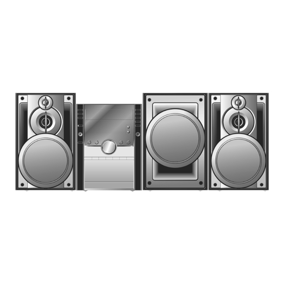
SA-AK750P
SA-AK750PC
Colour
(K)... Black Type
Frequency range
Sensitivity
80 W per channel (3 Ω)
S/N 26 dB
Antenna terminal(s)
80 W per channel (3 Ω)
Amplitude Modulation (AM)
Frequency range
160 W per channel (6 Ω)
Sensitivity
480 W
S/N 20 dB (at 1000 kHz)
Music Port input jack
Terminal
Sensitivity
110 W per channel (3 Ω)
Phone jack
Terminal
110 W per channel (3 Ω)
XM ready
n CASSETTE DECK SECTION
220 W per channel (6 Ω)
Track system
660 W
Heads
Record/playback
FM 20 stations
Erasure
AM 15 stations
Motor
Recording system
ORDER NO. MD0703010CE
CD Stereo System
87.9 to 107.9 MHz (200 kHz
87.5 to 108.0 MHz (100 kHz
520 to 1710 kHz (10 kHz step)
Stereo, 3.5 mm (1/8") jack
Stereo, 3.5 mm (1/8") jack
XM mini Tuner and Home Dock
Double gap ferrite head
© 2007 Matsushita Electric Industrial Co. Ltd.. All
rights
reserved.
Unauthorized
distribution is a violation of law.
A6
steps)
steps)
4.0 µV (IHF)
2.2 µV
75 Ω (unbalanced)
560 µV/m
100 mV, 4.7 kΩ
4 track, 2 channel
Solid permalloy head
DC servo motor
AC bias 100 kHz
copying
and
Advertisement
Table of Contents

Related Manuals for Panasonic SA-AK750P


Summary of Contents for Panasonic SA-AK750P
-
Page 1: Specifications
ORDER NO. MD0703010CE CD Stereo System SA-AK750P SA-AK750PC Colour (K)... Black Type Notes: This model’s CD mechanism changer unit is CRS1. Please refer to the original Service Manual (Order No. MD0509368C0) for this mechanism. Specifications n AMPLIFIER SECTION Frequency range 87.9 to 107.9 MHz (200 kHz... -
Page 2: Table Of Contents
SA-AK750P / SA-AK750PC Erase system AC erase 100 kHz I-Pod Cradle Tape speed 4.8 cm/s (1-7/8 ips) Supported audio file format Overall frequency response (+3, -6 dB) at DECK OUT (1) CD-Audio (CD-DA) NORMAL 35 Hz to 14 kHz (2) CD-R/RW (CD-DA, MP3 formatted disc) - Page 3 SA-AK750P / SA-AK750PC 10.6. Disassembly of Rear Panel Block 17.1. CD Servo Diagram 10.7. Disassembly of Main P.C.B. 17.2. Deck/ Deck Mechanism Diagram 10.8. Disassembly of Transformer P.C.B. 17.3. D-Port & Main Diagram 10.9. Disassembly of Power P.C.B. 17.4. Panel Diagram 10.10.
-
Page 4: Safety Precautions
SA-AK750P / SA-AK750PC 1 Safety Precautions 1.1. General Guidelines 1. When servicing, observe the original lead dress. If a short circuit is found, replace all parts which have been overheated or damaged by the short circuit. 2. After servicing, ensure that all the protective devices such as insulation barriers and insulation papers shields are properly installed. -
Page 5: Protection Circuitry
SA-AK750P / SA-AK750PC 1.3. Protection Circuitry The protection circuitry may have operated if either of the following conditions are noticed: · No sound is heard when the power is turned on. · Sound stops during a performance. The function of this circuitry is to prevent circuitry damage if, for example, the positive and negative speaker connection wires are “shorted”, or if speaker systems with an impedance less than the indicated rated impedance of the amplifier are used. - Page 6 SA-AK750P / SA-AK750PC caused by electro static discharge (ESD). 1. Immediately before handling any semiconductor component or semiconductor-equiped assembly, drain off any ESD on your body by touching a known earth ground. Alternatively, obtain and wear a commercially available discharging ESD wrist strap, which should be removed for potential shock reasons prior to applying power to the unit under test.
-
Page 7: Handling Precautions For Traverse Deck
SA-AK750P / SA-AK750PC 3 Handling Precautions For Traverse Deck The laser diode in the traverse deck (optical pickup) may break down due to potential difference caused by the static electricity of clothes or our human body. So, be careful of electrostatic breakdown during repair of the traverse deck (optical pickup). - Page 8 SA-AK750P / SA-AK750PC...
-
Page 9: Precaution Of Laser Diode
SA-AK750P / SA-AK750PC 4 Precaution of laser diode CAUTION: This unit utilizes a class 1 laser diode in the optical pickup unit . Invisible laser radiation is emitted from the optical pickup lens. Wavelength: 780nm When the unit is turned on: 1. -
Page 10: Warning
SA-AK750P / SA-AK750PC 5 Warning 5.1. Service caution based on legal restrictions 5.1.1. General description about Lead Free Solder (PbF) The lead free solder has been used in the mounting process of all electrical components on the printed circuit boards used for this equipment in considering the globally environmental conservation. -
Page 11: Accessories
SA-AK750P / SA-AK750PC 6 Accessories Remote Control FM Indoor Antenna AC Cord AM Loop Antenna... -
Page 12: Operation Procedures
SA-AK750P / SA-AK750PC 7 Operation Procedures 7.1. Main Unit Key Buttons Operations 7.2. Remote Control Key Buttons Operations... - Page 13 SA-AK750P / SA-AK750PC...
-
Page 14: New Features
SA-AK750P / SA-AK750PC 8 New Features 8.1. Using the Music Port This feature enables you to enjoy music from a portable audio equipment. With reference to page 15 of the operating instruction manual. -
Page 15: Using Xmョ Satellite Radio
SA-AK750P / SA-AK750PC 8.2. Using XM® Satellite Radio With reference to page 12 of the operating instruction manual. - Page 16 SA-AK750P / SA-AK750PC With reference to page 13 of the operating instruction manual.
-
Page 17: Using Ipod
SA-AK750P / SA-AK750PC 8.3. Using IPod With reference to page 16 of the operating instruction manual. - Page 18 SA-AK750P / SA-AK750PC With reference to page 17 of the operating instruction manual.
-
Page 19: Self Diagnosis And Special Mode Setting
SA-AK750P / SA-AK750PC 9 Self diagnosis and special mode setting This unit is equipped with functions for checking and inspecting namely: Self-Diagnostic and Test Mode. 9.1. Service Mode Summary Table The service modes can be activated by pressing various button combination on the main unit and remote control unit. Below is the... - Page 20 SA-AK750P / SA-AK750PC Item FL Display Key Operation Mode Name Description Front Key Doctor Mode To enter into Doctor (Display 1) In any mode: Mode for checking of 1. Press [ ] button on main unit various items and follow by [4] and [7] on remote control.
- Page 21 SA-AK750P / SA-AK750PC Item FL Display Key Operation Mode Name Description Front Key Tape Eject Test To check on the tape In doctor mode: eject function (For deck 1. Press [0] button on remote control. 1/2) FL Display Test To...
-
Page 22: Reliability Test Mode (Crs1 Mechanism)
SA-AK750P / SA-AK750PC Note: Microprocessor firmware refers to version number for microprocessor IC located on PANEL P.C.B.. It is subject to change which would be updated accordingly. ROM correction checksum refers to the HEX code that is displayed upon key buttons pressed if an EEPROM is loaded in the unit. -
Page 23: Error Code Table Display
SA-AK750P / SA-AK750PC 9.4. Error code Table Display Self-Diagnosis Function (refer Section 9.2) provides information on any problems occuring for the unit and its respective components by displaying the error codes. These error code such as U**, H** and F** are stored in memory and held unless it is... - Page 24 SA-AK750P / SA-AK750PC The error code is automatically display after entering into self-diagnostic mode. 9.4.1. Error Code Table for Deck Mechanism Error Code Diagnosis Contents Description of error Automatic FL Display Remarks Mode SW, plunger Normal operation during For deck mechanism unit.
- Page 25 SA-AK750P / SA-AK750PC Error Code Diagnosis Contents Description of error Automatic FL Display Remarks HOME Cam gear/gear Cam gear does not move to For CD changer unit (CRS1). assembly abnormal “HOME” position under Press [SINGLE CHANGE] on main unit following conditions for next error.
-
Page 26: Xm Satellite Radio Code Table
SA-AK750P / SA-AK750PC · Only the first 5 errors will be memorized (in backup memory). The subsequence error shall be ignored and not memorize. For system with EEPROM as memory backup,memory space in EEPROM is neccesary. 2. To display all error code memorized In CRS1 Self-Diagnostic mode, press [SINGLE CHANGE] to display subsequence error code. -
Page 27: Assembling And Disassembling
SA-AK750P / SA-AK750PC 10 Assembling and Disassembling 10.1. Caution Special Note: This model uses a new CD changer unit CRS1. In this following section does not contain the necessary disassembly & assembly information for the CD changer unit (CRS1) except the disasembly & assembly of traverse unit. Kindly refer to the original service manual for the CD changer unit. -
Page 28: Disassembly Flow Chart
SA-AK750P / SA-AK750PC 10.2. Disassembly flow chart The following chart is the procedure for disassembling the casing and inside parts for internal inspection when carrying out the servicing. To assemble the unit, reverse the steps shown in the chart as below. -
Page 29: Main Parts Location
SA-AK750P / SA-AK750PC 10.3. Main Parts Location... -
Page 30: Disassembly Of Top Cabinet
SA-AK750P / SA-AK750PC 10.4. Disassembly of Top Cabinet Step 1 Remove 3 screws on both sides on top cabinet. Step 2 Remove 5 screws at the rear. Step 3 Lift the sides of top cabinet outwards. Step 4 Push the top cabinet backwards to release catches. -
Page 31: Disassembly Of Rear Panel Block
SA-AK750P / SA-AK750PC Step 4 Lift the CD changer unit upwards to remove it. · Disassembly of Mecha Chassis Step 5 Remove 2 screws. Step 6 Remove the Mecha Chassis. Note: For disassembly & assembly of traverse unit, please refer to section 10.16 of this service manual.Please refer to original... - Page 32 SA-AK750P / SA-AK750PC · Disassembly of XM in P.C.B. Step 1 Remove 1 screw. · Disassembly of D-Port P.C.B. Step 1 Remove 2 screws. Step 2 Detach cable CN2810 at Main P.C.B.. Step 3 Detach FFC cables (CN2801 & CN2805) at Main P.C.B..
-
Page 33: Disassembly Of Main P.c.b
SA-AK750P / SA-AK750PC 10.7. Disassembly of Main P.C.B. · Follow the (Step 1) - (Step 5) of Item 10.4 · Follow the (Step 1) - (Step 4) of Item 10.5 · Follow the (Step 1) - (Step 4) of Item 10.6 Step 1 Detach FFC cables (CN2803 &... -
Page 34: Disassembly Of Power P.c.b
SA-AK750P / SA-AK750PC 10.9. Disassembly of Power P.C.B. · Follow the (Step 1) - (Step 5) of Item 10.4 · Follow the (Step 1) - (Step 4) of Item 10.5 · Follow the (Step 1) - (Step 4) of Item 10.6 ·... -
Page 35: Disassembly Of Front Panel Unit
SA-AK750P / SA-AK750PC Step 3 Remove up the heat sink sub assembly (with IC5501). Step 4 Remove screw and IC clip. Step 5 Remove IC5501 from the sub assembly. Caution: During assembly of the heat sink sub assembly (with IC5501) all soldering points is touch-up to avoid dry- joints. -
Page 36: Disassembly For Panel P.c.b
SA-AK750P / SA-AK750PC Step 5 Remove the front panel unit. Note: Ensure 2 claws located at the bottom chassis is seated into the 2 slots at bottom of front panel at 2 catches (one on each side) of bottom chassis to be aligned to front panel’s slot. -
Page 37: Disassembly Of Tact Switch P.c.b
SA-AK750P / SA-AK750PC Step 2 Remove Lid. Note: Do not misplace the spring. 10.12. Disassembly of Tact Switch P.C.B. · Follow the (Step 1) - (Step 5) of Item 10.4 · Follow the (Step 1) - (Step 4) of Item 10.5 ·... -
Page 38: Disassembly Of Deck P.c.b
SA-AK750P / SA-AK750PC Step 3 Tilt the cassette mechanism unit in the direction of Note: For disassembly of parts for deck mechanism unit, arrow (1), and then remove it in the direction of arrow (2). refer to Section 10.16. 10.14. Disassembly of Deck P.C.B. -
Page 39: Disassembly For Deck Mechanism
SA-AK750P / SA-AK750PC Step 3: Remove the traverse unit as arrow shown. · Assembly of Traverse Unit Step 2: Push the traverse slide plate as arrow shown to lock the traverse unit. Step 1: Turn over the unit and install the traverse unit. - Page 40 SA-AK750P / SA-AK750PC 10.16.1. Replacement of Pinch Roller and Head Block...
- Page 41 SA-AK750P / SA-AK750PC 10.16.2. Replacement of Motor, Capstan Belt A, Capstan Belt B, and Winding Belt...
-
Page 42: Disassembly Of Deck Mechanism P.c.b
SA-AK750P / SA-AK750PC 10.17. Disassembly of Deck Mechanism P.C.B. · Follow the (Step 1) - (Step 4) of Item 10.4 · Follow the (Step 1) - (Step 4) of Item 10.5 · Follow the (Step 1) - (Step 5) of Item 10.10 ·... -
Page 43: Disassembly Of Cassette Lid
SA-AK750P / SA-AK750PC 10.18. Disassembly of cassette lid · Follow the (Step 1) - (Step 4) of Item 10.4 · Follow the (Step 1) - (Step 4) of Item 10.5 · Follow the (Step 1) - (Step 5) of Item 10.10 ·... - Page 44 SA-AK750P / SA-AK750PC Step 2 Push the lever upward and open the cassette lid. Remove the cassette tape. Note: Follow 10.18 Disassembly of cassette lid (Step1) to (Step 3). Remove the cassette tape.
-
Page 45: Service Fixture And Tools
SA-AK750P / SA-AK750PC 11 Service Fixture and Tools Service Tools Extension FFC (A) Deck P.C.B. - Main P.C.B. REEX0485 (14 Pins) 12 Service Positions Note: For description of the disassembly procedures, see the Section 10. 12.1. Checking and Repairing of Main P.C.B. -
Page 46: Checking And Repairing Of Transformer P.c.b
SA-AK750P / SA-AK750PC 12.2. Checking and Repairing of Transformer P.C.B. 12.3. Checking and Repairing of Panel, Deck & Deck Mechanism P.C.B. -
Page 47: Checking And Repairing Of Power P.c.b
SA-AK750P / SA-AK750PC 12.4. Checking and Repairing of Power P.C.B. -
Page 48: Procedure For Checking Operation Of Individual Parts Of Deck Mechanism Unit
SA-AK750P / SA-AK750PC 13 Procedure for Checking Operation of Individual Parts of Deck Mechanism Unit 13.1. Operation Check with Cassette Tape 1. Pull up the EJECT lever using a rubber band. (Fig. 6) 2. Supply DC5V to MOTOR. (→ MOTOR rotates.) (Fig. 5) 3. - Page 49 SA-AK750P / SA-AK750PC Fig. 7...
-
Page 50: Measurement And Adjustments
SA-AK750P / SA-AK750PC 14 Measurement And Adjustments 14.1. Cassette Deck Section 14.1.1. Requirements · Test tape (QZZCFM) (QZZCWAT) · Normal blank cassette tape (QZZCRA) · Digital frequency counter · Oscilloscope · Electrical voltmeter · Headphone jack output jig (Fig 8) 14.1.2. - Page 51 SA-AK750P / SA-AK750PC Fig. 10 Fig. 11 14.1.5. Bias Voltage Check 1. Connect an electrical voltmeter. (Fig 12) (Fig 9 for location of test points) 2. Set the function to “TAPE” position. 3. Insert a normal blank cassette tape (QZZCRA).
-
Page 52: Voltage And Waveform Chart
SA-AK750P / SA-AK750PC 15 Voltage and Waveform Chart Note: Circuit voltage and waveform described herein shall be regarded as reference information when probing defect point, because it may differ from an actual measuring value due to difference of Measuring instrument and its measuring condition and product itself. -
Page 53: Power P.c.b. & Transformer P.c.b
SA-AK750P / SA-AK750PC 15.2. Power P.C.B. & Transformer P.C.B. 15.3. Panel P.C.B. -
Page 54: Main P.c.b
SA-AK750P / SA-AK750PC 15.4. Main P.C.B. -
Page 55: Xm P.c.b
SA-AK750P / SA-AK750PC 15.5. XM P.C.B. 15.6. Deck P.C.B. -
Page 56: Waveform Chart
SA-AK750P / SA-AK750PC 15.7. Waveform Chart... -
Page 57: Wiring Connection Diagram
SA-AK750P / SA-AK750PC 16 Wiring Connection Diagram JK2803 CN2810 9 ..1 CN3601 12 . . . 2 H5104 13 ..1 CN3400 CN3100 TUNER MOTOR PACK CN2809 POWER P.C.B. SOLDER SIDE CN2801 MAIN P.C.B. - Page 58 SA-AK750P / SA-AK750PC...
-
Page 59: Block Diagram
SWITCH PROCESSOR/ TO MAIN CN7002 CN2801 DIGITAL FILTER (1/2) 3.3V 3.3V 3.3V 3.3V D/A CONVERTER PC1 4 MUTE CN7002 CN2801 [CH1] LCH OUT 3.3V TO MAIN (2/2) CN7002 CN2801 RCH OUT MUTE PC2 2 [CH2] SA-AK750P/PC CD SERVO BLOCK DIAGRAM... -
Page 60: Deck/ Deck Mechanism Diagram
: CD-DA (AUDIO/VIDEO) SIGNAL LINE : AM SIGNAL LINE : FM/AM/XM SIGNAL LINE : TAPE RECORD SIGNAL LINE : FM SIGNAL LINE : AUX/IPOD SIGNAL LINE : TAPE PLAYBACK SIGNAL ( ) Indicates the Pin No. of Right Channel. SA-AK750P/PC DECK/DECK MECHANISM BLOCK DIAGRAM... -
Page 61: D-Port & Main Diagram
FROM OPTION PORT C0CBCDG00003 CN3400 CN2401 CN2401 VER.1 (TO DOCK) CN2401 CN3400 CN2401 PCONT PCONT CN2401 CN3400 CN2401 CN3400 CN2401 Q3500 TO D-PORT D3501-D3505 CN3400 CN2401 CN2401 Vout SWITCH CN2401 SA-AK750P/PC D-PORT / MAIN 1/2 DIAGRAM CN3400 CN2401 D-PORT P.C.B... - Page 62 QR3105 QR3106 SWITCH SWITCH Q2803 IC4000 C0DBZGC00067 RESET (MICRO-P) 3.3 REGULATOR SWITCH Q3601 SWITCH STBY Q2950 D2936 DECK SUPPLY DVREF CONTROL SWITCH IC2872 C0CBAHG000011 AV REGULATOR IC Q2950 DECK SUPPLY CONTROL SWITCH 3.3V D2811 D2813 D3400 SA-AK750P/PC MAIN 2/2 DIAGRAM...
-
Page 63: Panel Diagram
SA-AK750P / SA-AK750PC 17.4. Panel Diagram FL6602 A2BD00000171 FL DISPLAY 5-11 25-40 TO TRANSFORMER 31-41 14-29 IC6601 C0HBB0000057 FL DRIVER TO MAIN (2/2) Z6481 REMOTE SENSOR JK6751 TO MAIN M.PORT (1/2) S6201-S6207 TO MAIN (2/2) JK6551 TO MAIN HEADPHONE (1/2) -
Page 64: Power Diagram
SA-AK750P / SA-AK750PC 17.5. Power Diagram JK5101 IC5301 SPEAKER C1AA00000755 2CH DIGITAL AMP L5301 OUT1 10 RCH.H IN1+ SPEAKER RCH.HIGH TO MAIN OUT2 14 IN1- RCH.L (1/2) SPEAKER IN2+ RCH.LOW IN2- Q5153 MODE 1 OSC SWITCH VDDA1 20 TO MAIN... -
Page 65: Xm/ Transformer Diagram
TO MAIN (2/2) LINKACTIVE Q5953 RL5950 SC_TX_OUT PCONT SWITCH SC_RX_IN TO PANEL Q5952 T5951 ANT_REV SYNCHRONISATION SWITCH RST- D5966 JK5950 L5950 C0DBZYE00002 POWER SUPPLY Z5950 5.3V D5951, Q5950 D5952 D5963 TO MAIN VOLTAGE (1/2) REGULATOR SA-AK750P/PC XM / TRANSFORMER DIAGRAM... - Page 66 SA-AK750P / SA-AK750PC...
-
Page 67: Notes Of Schematic Diagram
SA-AK750P / SA-AK750PC 18 Notes Of Schematic Diagram (All schematic diagrams may be modified at any time with : Tape Record signal line the development of new technology) : Tape Playback signal line Notes: S971: Mode switch. : XM, FM/AM/XM, FM/AM signal line S972: Half switch. - Page 68 SA-AK750P / SA-AK750PC...
-
Page 69: Schematic Diagram
12 11 R7220 R7330 W7002 W7004 5.6K C7335 X7201 C7315 IC7002 0.47 H2B169500005 BA5948FPE2 C7334 4 CH DRIVE IC C7338 10V220 0.056 R7323 R7331 3.3k R7325 R7315 3.3k R7332 R7335 M7302 M7301 TRAVERSE MOTOR SPINDLE MOTOR SA-AK750P/PC CD SERVO CIRCUIT... -
Page 70: B) Xm Module Circuit
XM SAT RADIO DRIVER 100mA (CN3100) SC_RXD SC_RATE IN SCHEMATIC SC_TXD ANT_REV DIAGRAM-4 [12]SLAVE_SEL [25]VSS ANT_REV [13]I2S_RATE 4.7K DTIC_RST RST- DGND DGND 16 17 18 19 5.3V H0A451500001 5.3V 5.3V 500mA PWR_CTRL J0JHC0000107 C0DBZYE00002 POWER SUPPLY SA-AK750P/PC XM MODULE CIRCUIT... -
Page 71: C) Main Circuit
SA-AK750P / SA-AK750PC 19.3. (C) Main Circuit SCHEMATIC DIAGRAM - 3 MAIN CIRCUIT : CD SIGNAL : TAPE PLAYBACK SIGNAL LINE : FM/AM/XM SIGNAL LINE : MAIN SIGNAL LINE : AUX/IPOD SIGNAL LINE : +B SIGNAL LINE : TAPE RECORD SIGNAL LINE... - Page 72 SA-AK750P / SA-AK750PC SCHEMATIC DIAGRAM - 4 MAIN CIRCUIT : +B SIGNAL LINE : FM/AM/XM SIGNAL LINE : MAIN SIGNAL LINE : IPOD SIGNAL LINE R2334 R2335 R2331 C2333 W587 C2331 Q2317,Q2417 6800p R2333 B1ABCF000176 MUTING SWITCH CN2809 F_HOP R2316 2.2k...
- Page 73 SA-AK750P / SA-AK750PC SCHEMATIC DIAGRAM - 5 MAIN CIRCUIT : +B SIGNAL LINE : FM/AM SIGNAL LINE : MAIN SIGNAL LINE : IPOD SIGNAL LINE : CD SIGNAL LINE W658 D2811 B0ADCJ000020 R2894 R2121 W617 3.3k TO MAIN SECTION (1/4) C2121 +3.3V...
- Page 74 SA-AK750P / SA-AK750PC SCHEMATIC DIAGRAM - 6 MAIN CIRCUIT : +B SIGNAL LINE : MAIN SIGNAL LINE : AUX SIGNAL LINE TO MAIN SECTION (2/4) IDCDET C2940 0.1u Q2942 R2940 B1ACKD000006 820k FAN MOTOR ON/OFF SWITCH Q2942 MOT_12V TO FAN...
-
Page 75: D) Panel Circuit
SA-AK750P / SA-AK750PC 19.4. (D) Panel Circuit SCHEMATIC DIAGRAM - 7 PANEL CIRCUIT :+B SIGNAL LINE : MAIN SIGNAL LINE : AUX SIGNAL LINE TRANSFORMER CIRCUIT (CN5951) IN SCHEMATIC DIAGRAM-12 H6555 R6631 W924 D6301 B0ACCK000005 R6632 GND2 SYS6V SYS6V GND3... -
Page 76: E) Sub Panel Circuit, (F) D-Port Circuit & (I) Deck Mechanism Circuit
R6307 2.7K S6108 2.7K SUBW C6492 C6491 100P 100P DISPLAY R6108 S6307 4.7K R6308 R6310 4.7K H.BASS S6308 COM B R6309 6.8K PRESENT EQ S6309 R972 VR6491 R973 EVEKE2F3024B VOLUME JOG IC971 CNB13030R2AU PHOTO INTERUPTOR SA-AK750P/PC SUB PANEL/D-PORT/DECK MECHANISM CIRCUIT... -
Page 77: G) Power Circuit
SA-AK750P / SA-AK750PC 19.6. (G) Power Circuit SCHEMATIC DIAGRAM -9 POWER CIRCUIT : MAIN SIGNAL LINE : +B SIGNAL LINE : -B SIGNAL LINE Q5154 2SB0709AHL Q5173 R5154 W1102 PCONT SWITCH B1ABCF000176 R5153 SWITCH R5148 IC5301 IC5401 IC5501 C5121 R5174... - Page 78 SA-AK750P / SA-AK750PC SCHEMATIC DIAGRAM - 10 POWER CIRCUIT : MAIN SIGNAL LINE : +B SIGNAL LINE : -B SIGNAL LINE SUBWOOFER- SUBWOOFER+ C5335 0.015 SUBWOOFER- SUBWOOFER SUBWOOFER+ C5343 JK5102 0.015 L5604 C5334 0.015 G0B9R5K00001 LEFT LOW + LEFT LOW -...
-
Page 79: F) Deck Circuit
SA-AK750P / SA-AK750PC 19.7. (F) Deck Circuit SCHEMATIC DIAGRAM - 11 DECK CIRCUIT : TAPE RECORD SIGNAL LINE : TAPE PLAYBACK SIGNAL LINE : +B SIGNAL LINE C1105 470P R1103 C1122 0.01 R1101 C1104 0.027 CP1301 ERASE Q1101,Q1201 ERASE HEAD... -
Page 80: K) Transformer Circuit
SA-AK750P / SA-AK750PC 19.8. (K) Transformer Circuit SCHEMATIC DIAGRAM - 12 TRANSFORMER CIRCUIT :+B SIGNAL LINE FP5940 C5940 50V1000u C5960 0.1u +VCC1 C5920 50V1000u +VCC1 FP5920 -VCC1 T5950 POWER CIRCUIT -VCC1 G4CYAYY00147 (H5104) IN MAIN TRANSFORMER SCHEMATIC DIAGRAM-10 SUB+B CN5950... -
Page 81: Printed Circuit Board
SA-AK750P / SA-AK750PC 20 Printed Circuit Board Note: Circuit board diagrams may be modified at any time with the development of new technology. -
Page 82: A) Cd Servo P.c.b., (H) Deck P.c.b., & (I) Deck Mechanism P.c.b
SA-AK750P / SA-AK750PC 20.1. (A) CD Servo P.C.B., (H) Deck P.C.B., & (I) Deck Mechanism P.C.B. CD SERVO P.C.B (REPV0111A) DECK P.C.B (REPV0134B) (RF) TP51 C7227 W1930 TP19 W7014 Q1309 CN1305 Q1310 TP14 C7204 W7015 C7226 W1909 W1935 R7212 TP18... -
Page 83: C) Main P.c.b
SA-AK750P / SA-AK750PC 20.2. (C) Main P.C.B. MAIN P.C.B (REPV0130A) Q2554 R2556 R2447 C2705 R2702 R2941 R2565 R2561 W573 C2941 R2721 R2446 C2312 R2564 R2722 C2552 R2145 Q2441 R2560 W277 R2705 R2703 R2557 R2944 Q2552 C2722 R2315 C2703 C2944 Q2555... -
Page 84: D) Panel P.c.b
SA-AK750P / SA-AK750PC 20.3. (D) Panel P.C.B. PANEL P.C.B (REPV0131A) S6103 S6201 (CD1) (OPEN/CLOSE) R6481 R6105 R6202 S6102 S6202 (CD2) (MULTI CHANGE) W807 W808 W809 S6203 R6102 (CD3) L6553 L6551 W909 S6104 (SINGLE CHANGE) (CD4) S6204 W840 L6552 W911 W1017... -
Page 85: B) Xm Module P.c.b. (Side A & B), (E) Sub Panel P.c.b F) D-Port P.c.b
SA-AK750P / SA-AK750PC 20.4. (B) XM Module P.C.B. (Side A & B), (E) Sub Panel P.C.B. & (F) D-Port P.C.B. D-PORT P.C.B (REPV0129A) SUB PANEL P.C.B (REPV0131A) D6462 JW6001 CN806A (VOL. LED) S6304 S6305 R6302 R6303 (TUNER) (EXT_IN) R6457 WA3004... -
Page 86: G) Power P.c.b
SA-AK750P / SA-AK750PC 20.5. (G) Power P.C.B. POWER P.C.B (REPV0133G) H5104 C5114 Q5201 Q5202 C5115 C5103 IC5201 W1003 C5210 W1005 C5208 W1092 X5201 W1099 R5204 R5514 R5205 C5172 C5701 R5206 W1094 W1095 W1093 C5102 W1007 C5205 R5103 R5209 R5419 W1096... -
Page 87: J) Transformer P.c.b
SA-AK750P / SA-AK750PC 20.6. (J) Transformer P.C.B. TRANSFORMER P.C.B (REPV0132A) T5951 125V 4A (SUB TRANSFORMER) L5950 C5953 Q5950 J5955 R5952 D5972 Z5950 C5951 C5952 D5952 RL5950 C5954 JK5950 Q5952 W5914 Q5953 W5915 CN5951 R5958 AC IN ~ D5970 W5905 R5951... - Page 88 SA-AK750P / SA-AK750PC...
-
Page 89: Illustration Of Ics, Transistors And Diodes
SA-AK750P / SA-AK750PC 21 Illustration of ICs, Transistors and Diodes C0AABB000125 C0ABBB000244 (8P) C0CBAHG00011 C1AA00000612 C0FBBY000027 (16P) C1BB00001121 (100P) C0DBZYE00002 (8P) MN6627954MA (100P) C1AB00002670 (48P) C0HBB0000057 (44P) C2CBYY000424 (100P) C0DAZYY00005 C0CBCDG00003 C0DBZGC00067 AN7326K (26P) BA5948FPE2 C0GAG0000007 C0JBAB000011(14P) CNB13030R2AU B1AAKD000014 2SD09650RA... -
Page 90: Terminal Function Of Ic's
SA-AK750P / SA-AK750PC 22 Terminal Function of IC's 22.1. IC7001 (MN6627954MA) Servo Processor,Digital Signal Processor/Digital filter and D/A Converter Pin No. Mark Function Pin No. Mark Function DRAM address signal O/P 11 IREF Reference I/P DRAM address signal O/P 9... -
Page 91: Ic7003 (Ba5948Fpe2) Ic 4Ch Drive
SA-AK750P / SA-AK750PC 22.2. IC7003 (BA5948FPE2) IC 4CH Drive Pin No. Mark Function Pin No. Mark Function Motor Driver 92 Input Motor Drive (3) reverse - action output Turntable Motor Drive Signal (“L”:ON) Motor Drive (3) forward - action output... - Page 92 SA-AK750P / SA-AK750PC Pin No. Mark Function OPEN_SW Open switch for CRS1 CRS1 motor CW CRS1 motor CCW ST_SW Stock switch for CRS1 PLAY_SW Play switch for CRS1 PLUNGER Plunger for CRS1 Region Setting VOL_JOG Volume jog D-PORT P-CONT D-Port P-CONT...
-
Page 93: Exploded Views
SA-AK750P / SA-AK750PC 23 Exploded Views 23.1. Cabinet Parts Location... - Page 94 SA-AK750P / SA-AK750PC...
-
Page 95: Deck Mechanism Parts Locations (Raa4403-S)
SA-AK750P / SA-AK750PC 23.2. Deck Mechanism Parts Locations (RAA4403-S) -
Page 96: Packaging
SA-AK750P / SA-AK750PC 23.3. Packaging... -
Page 97: Replacement Parts List
SA-AK750P / SA-AK750PC 24 Replacement Parts List Notes: · Important safety notice: Components identified by mark have special characteristics important for safety. Furthermore, special parts which have purposes of fire-retardent (resistors), high-quality sound (capacitors), low noise (resistors), etc are used. - Page 98 SA-AK750P / SA-AK750PC Ref. No. Part No. Part Name & Description Remarks Ref. No. Part No. Part Name & Description Remarks RXF0061-1 FLYWHEEL F ASS’Y Q1310 B1AAGC000006 TRANSISTOR RXG0040 FF RELAY GEAR ASS’Y Q1312 B1ABCF000011 TRANSISTOR RMK0283A-2 SUB-CHASSIS Q1314 B1GDCFGH0002...
- Page 99 SA-AK750P / SA-AK750PC Ref. No. Part No. Part Name & Description Remarks Ref. No. Part No. Part Name & Description Remarks D2552 B0BC2R4A0006 DIODE VARIABLE RESISTOR D2583 B0BC9R000008 DIODE D2603 B0BC9R000008 DIODE VR6491 EVEKE2F3024B VR VOLUME JOG D2803 B0ACCK000005 DIODE...
- Page 100 SA-AK750P / SA-AK750PC Ref. No. Part No. Part Name & Description Remarks Ref. No. Part No. Part Name & Description Remarks L5301 G0B185LA0002 COIL JK6551 K2HC103A0024 JK HP L5401 G0B185LA0002 COIL JK6751 K2HC1YYA0002 JK MUSIC PORT L5402 J0JKB0000037 FILTER L5403...
- Page 101 SA-AK750P / SA-AK750PC Ref. No. Part No. Part Name & Description Remarks Ref. No. Part No. Part Name & Description Remarks W641 ERJ6GEY0R00V CHIP JUMPER W7001 D0GDR00JA017 CHIP JUMPER W642 ERJ6GEY0R00V CHIP JUMPER W7002 D0GDR00JA017 CHIP JUMPER W643 ERJ6GEY0R00V CHIP JUMPER...
- Page 102 SA-AK750P / SA-AK750PC Ref. No. Part No. Part Name & Description Remarks Ref. No. Part No. Part Name & Description Remarks D0GB470JA008 47 1/16W R1344 D0GB273JA008 27K 1/16W D0GB470JA008 47 1/16W R1345 D0GB102JA008 1K 1/16W D0GB470JA008 47 1/16W R1371 D0GB223JA007...
- Page 103 SA-AK750P / SA-AK750PC Ref. No. Part No. Part Name & Description Remarks Ref. No. Part No. Part Name & Description Remarks R2345 D0GB153JA008 15K 1/16W R2701 D0GB102JA008 1K 1/16W R2346 D0GB332JA007 3.3K 1/16W R2702 D0GB102JA008 1K 1/16W R2347 D0GB1R0JA007 1 1/16W...
- Page 104 SA-AK750P / SA-AK750PC Ref. No. Part No. Part Name & Description Remarks Ref. No. Part No. Part Name & Description Remarks R2947 D0AF270JA039 27 1/4W R5127 D0GB471JA041 470 1/16W R2948 D0GB101JA007 100 1/16W R5132 D0AF331JA039 330 1/4W R2949 D0GB473JA041 47K 1/16W...
- Page 105 SA-AK750P / SA-AK750PC Ref. No. Part No. Part Name & Description Remarks Ref. No. Part No. Part Name & Description Remarks R5526 ERJ6GEYJ105V 1M 1/10W R7331 D0GB223JA008 22K 1/16W R5950 ERC12UGK335D 3.3M 1/2W R7332 D0GB102JA008 1K 1/16W R5951 D0AE332JA048 3.3K 1/4W...
- Page 106 SA-AK750P / SA-AK750PC Ref. No. Part No. Part Name & Description Remarks Ref. No. Part No. Part Name & Description Remarks C1304 F2A1H4R7A014 4.7 50V C2412 F1H1A105A025 1 10V C1305 F2A1C330A234 33 16V C2413 F1H1H470A230 47P 50V C1307 ECA1AAK221XQ 220 10V...
- Page 107 SA-AK750P / SA-AK750PC Ref. No. Part No. Part Name & Description Remarks Ref. No. Part No. Part Name & Description Remarks C3001 ECJ1VB1H104K 0.1 50V C5305 F1H1H331A013 330P 50V C3100 F1H1H102A219 1000P 50V C5306 ECJ1VB1A474K 0.47 10V C3101 F1H1H102A219 1000P 50V...
- Page 108 SA-AK750P / SA-AK750PC Ref. No. Part No. Part Name & Description Remarks Ref. No. Part No. Part Name & Description Remarks C5505 ECJ1VB1H331K 330P 50V C7203 F2A0J221A200 220 6.3V C5506 ECJ1VB1A474K 0.47 10V C7204 ECJ1VB1C104K 0.1 16V C5508 ECJ1VB1H104K 0.1 50V...
Need help?
Do you have a question about the SA-AK750P and is the answer not in the manual?
Questions and answers