Table of Contents
Advertisement
QQ
3 7 63 1515 0
SERVICE MANUAL
Ver. 1.2 2007. 08
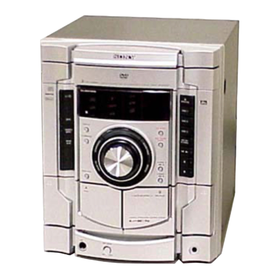
• HCD-GNZ55D is the tuner,
deck, DVD and amplifier
section in MHC-GNZ55D.
TE
L 13942296513
Amplifier section
The following measured at AC 120, 127, 220, 240 V,
50/60 Hz
DIN power output (rated)
40 W + 40 W
(4 ohms at 1 kHz, DIN)
Continuous RMS power output (reference)
60 W + 60 W
(4 ohms at 1 kHz, 10%
THD)
Inputs
MIC (phone jack):
Sensitivity 1 mV,
impedance 10 kilohms
Outputs
VIDEO OUT (phono jack):
max. output level
1 Vp-p, unbalanced, Sync
negative load impedance
75 ohms
PHONES (stereo mini jack):
Accepts headphones of
8 ohms or more
FRONT SPEAKER:
Use only the supplied speakers
www
.
Sony Corporation
9-887-296-03
2007H04-1
Personal Audio Division
© 2007. 08
Published by Sony Techno Create Corporation
http://www.xiaoyu163.com
HCD-GNZ55D
DVD
Section
Tape Deck
Section
x
ao
u163
y
i
http://www.xiaoyu163.com
2 9
8
Model Name Using Similar Mechanism
DVD Mechanism Type
Optical Pick-up Name
Model Name Using Similar Machanism
Q Q
3
6 7
1 3
1 5
SPECIFICATIONS
Disc player section
System
Laser
Frequency response
Video color system format
co
.
9 4
2 8
E Model
HCD-GNZ7D/GNZ8D/GNZ9D
CDM74HF-DVBU101//C
KHM-310CAB/C2NP
NEW
0 5
8
2 9
9 4
2 8
Compact disc and digital
audio and video system
Semiconductor laser
(DVD: λ=650 nm,
CD: λ=790 nm)
Emission duration:
continuous
DVD (PCM 48 kHz):
2 Hz – 22 kHz (±1 dB)
CD: 2 Hz – 20 kHz (±0.5 dB)
Latin American model:
NTSC
Other models: NTSC, PAL
– Continued on next page –
m
DVD DECK RECEIVER
9 9
9 9
1
Advertisement
Table of Contents

Related Manuals for Sony HCD-GNZ55D


Summary of Contents for Sony HCD-GNZ55D
-
Page 1: Service Manual
HCD-GNZ55D 3 7 63 1515 0 SERVICE MANUAL E Model Ver. 1.2 2007. 08 • HCD-GNZ55D is the tuner, deck, DVD and amplifier section in MHC-GNZ55D. Model Name Using Similar Mechanism HCD-GNZ7D/GNZ8D/GNZ9D DVD Mechanism Type CDM74HF-DVBU101//C Section Optical Pick-up Name... - Page 2 COMPONENTS IDENTIFIED BY MARK 0 OR DOTTED LINE WITH MARK 0 ON THE SCHEMATIC DIAGRAMS AND IN THE PARTS LIST ARE CRITICAL TO SAFE OPERATION. REPLACE THESE COMPONENTS WITH SONY PARTS WHOSE PART NUMBERS APPEAR AS SHOWN IN THIS MANUAL OR IN SUPPLEMENTS PUBLISHED BY SONY.
- Page 3 HCD-GNZ55D Ver. 1.1 3 7 63 1515 0 Notes on Chip Component Replacement NOTES ON LASER DIODE EMISSION CHECK • Never reuse a disconnected chip component. The laser beam on this model is concentrated so as to be focused on •...
- Page 4 HCD-GNZ55D 3 7 63 1515 0 MODEL IDENTIFICATION • Abbreviation : 240 V AC area in E model – BACK PANEL – E12 : 220-240 V AC area in E model E13 : 220-230 V AC area in E model...
-
Page 5: Table Of Contents
HCD-GNZ55D 3 7 63 1515 0 TABLE OF CONTENTS 1. GENERAL 6-9. Printed Wiring Board — DMB15 Section — ....36 6-10. Schematic Diagram — DMB15 Section (1/5) — ..... 38 Main Unit ................6 6-11. Schematic Diagram — DMB15 Section (2/5) — ..... 39 Remote Control ............... -
Page 6: General
HCD-GNZ55D SECTION 1 GENERAL 3 7 63 1515 0 This section is extracted from instruction manual. List of button locations and reference pages How to use page 104 to 106 Illustration number Use this page to find the location of buttons and other TAPE A/B ef (60–62, 72, 75, 76) - Page 7 HCD-GNZ55D 3 7 63 1515 0 Top view Front view 2 34 5 6 L 13942296513 whwg continued u163 http://www.xiaoyu163.com...
-
Page 8: Remote Control
46–50, 59) a reference when operating the system. PICTURE NAVI 6 (35, 36, 41) This button is used to operate a Sony TV. For PRESET + qh (57–59) details, see “Operating a Sony TV with the remote” PRESET – wd (57–59) on page 17. -
Page 9: Disassembly
HCD-GNZ55D SECTION 2 DISASSEMBLY 3 7 63 1515 0 Note : Disassemble the unit in the order as shown below. 2-1. CABINET STEEL CASE (Page 10) 2-2. LOADING PANEL 2-9. TAPE MECHANISM DECK (Page 10) (Page 14) 2-3. FRONT PANEL SECTION 2-10. - Page 10 HCD-GNZ55D 3 7 63 1515 0 Note : Follow the disassembly procedure in the numerical order given. 2-1. CABINET STEEL CASE 6 two screws (+BVTP 3 × 8) 0 cabinet steel case 4 screw 5 three screws (+BVTP 3 × 8)
- Page 11 HCD-GNZ55D 3 7 63 1515 0 2-3. FRONT PANEL SECTION 5 CN205 (6P) 6 CN503 (3P) 7 screw (tapping screw) 4 CN121 (3P) 8 screw (tapping screw) 3 CN131 (8P) qa front panel section 1 wire (flat type) (11 core)
- Page 12 HCD-GNZ55D 3 7 63 1515 0 2-5. BACK PANEL SECTION 2 two screws (+BVTP 3 × 8) 8 back panel section 3 screw (+BVTP 3 × 8) 4 two screws 1 connector (9 core) (+BVTP 3 × 8) 5 screw (+BVTP 3 ×...
-
Page 13: Power Unit
HCD-GNZ55D 3 7 63 1515 0 2-7. SPEAKER BOARD, S-MASTER BOARD 7 two screws (+BVTT 3 × 6 (sumitite)) 8 heat sink assy 4 CN502 (6P) 6 two screws (+BVTT 3 × 6 (sumitite)) 1 CN1501 (4P) 5 two screws (+BVTT 3 ×... -
Page 14: Tape Mechanism Deck
HCD-GNZ55D 3 7 63 1515 0 2-9. TAPE MECHANISM DECK 2 two screws (+BVTP 2.6 (3CR)) 3 two screws (+BVTP 2.6 (3CR)) 4 two screws (+BVTP 2.6 (3CR)) 1 wire (flat type) (11 core) 5 tape mechanism deck L 13942296513 2-10. -
Page 15: Mic Board
HCD-GNZ55D 3 7 63 1515 0 2-11. MIC BOARD 4 bracket (TC) 1 four screws (+BVTP 2.6 (3CR)) 2 bracket (pivot) 5 MIC board 3 three screws (+BVTP 3 × 8) L 13942296513 2-12. VIDEO BOARD 1 wire (flat type) (5 core) -
Page 16: Dmb15 Board
HCD-GNZ55D 3 7 63 1515 0 2-13. DMB15 BOARD qs screw (+BVTP 3 × 8) qd cover (CDM) 0 screw qa two screws (+BVTP 3 × 8) (+BVTP 3 × 8) 9 bracket mediatek 2 wire (flat type) (24 core) -
Page 17: Motor (Tb) Board
HCD-GNZ55D 3 7 63 1515 0 2-15. MOTOR (TB) BOARD 2 stopper table assy 2 stopper 6 table motor assy (M741) 4 MOTOR (TB) board 5 Remove the two solders of motor. 3 two screws (+BTTP (M2.6)) L 13942296513 2-16. -
Page 18: Sw Board, Driver Board
HCD-GNZ55D 3 7 63 1515 0 2-17. PICK-UP UNIT 5 two insulators 2 two insulator screws 3 two insulator screws 6 pick-up unit 4 two insulators 7 holder (310) 1 floating screw (+PTPWH M2.6) L 13942296513 2-18. SW BOARD, DRIVER BOARD... -
Page 19: Test Mode
HCD-GNZ55D SECTION 3 TEST MODE 3 7 63 1515 0 [PANEL TEST MODE] • Check of Amplifier 1. Press [EQ BAND/MEMORY] button repeatedly until a message • This mode is used to check the fluorescent indicator tube, LEDs, keys, VOLUME jog, model, destination, software version and “GEQ MAX”... - Page 20 HCD-GNZ55D 3 7 63 1515 0 Procedure: [DVD COLOR SYSTEM] 1. Press button to turn on the system. • This mode let you change the color system of the video output 2. Press [TUNER/BAND] button repeatedly to select the “AM”.
- Page 21 HCD-GNZ55D Ver. 1.2 3 7 63 1515 0 • TEST DISC LIST Manual Adjust Be sure to use the DVD disc that matches the signal standards of your region. 1. Track Balance Adjust: • CD 2. Track Gain Adjust: YEDS-18 (Part No.: 3-702-101-01)
- Page 22 HCD-GNZ55D Ver. 1.2 3 7 63 1515 0 • Time of error code Emg.History Check This is the laser time when an error occurred. Laser Hours 999h 59min Example of Error code 999h 59min 1. 01 05 04 04 00 92 46 00 1.
-
Page 23: Mechanical Adjustments
HCD-GNZ55D Ver. 1.2 SECTION 4 MECHANICAL ADJUSTMENTS 3 7 63 1515 0 To return to the Top Menu of Remocon Diagnosis Menu Precaution Press [0] button on the remote commander. 1. Clean the following parts with a denatured alcohol-moistened swab: •... -
Page 24: Electrical Adjustments
HCD-GNZ55D Ver. 1.2 SECTION 5 ELECTRICAL ADJUSTMENTS 3 7 63 1515 0 Checking Location: DMB15 board (Side A) DVD SECTION When the optical pick-up assy is replaced, perform the “Execute DMB15 BOARD (SIDE A) IOP Measurement”. Execute IOP Measurement (See page 21) - Page 25 HCD-GNZ55D 3 7 63 1515 0 3. Mode: Playback DECK SECTION 0 dB=0.775 V test tape 1. Demagnetize the record/playback head with a head P-4-A063 demagnetizer. oscilloscope (6.3 kHz, –10 dB) 2. Do not use a magnetized screwdriver for the adjustments.
- Page 26 HCD-GNZ55D 3 7 63 1515 0 MEMO L 13942296513 u163 http://www.xiaoyu163.com...
-
Page 27: Diagrams
HCD-GNZ55D SECTION 6 DIAGRAMS 3 7 6 3 1 5 1 5 0 6-1. BLOCK DIAGRAM — RF/SERVO SECTION — DVDRFIP DVDA DVDB DETECTOR DVDC DVDD 8 NA 9 NB CD/DVD RF AMP, FOCUS/TRACKING ERROR AMP DVD SYSTEM PROCESSOR... -
Page 28: Block Diagram - Video Section
HCD-GNZ55D 3 7 6 3 1 5 1 5 0 6-2. BLOCK DIAGRAM — VIDEO SECTION — MAIN YUV3 SECTION (Page 29) D/A CONVERTER IC301 14 SDTI1 ASDAT0 15 SDTI2 ASDAT1 ASDAT2 16 SDTI3 IC3771 ASDAT4 13 SDTI4 LOUT4+... -
Page 29: Block Diagram - Main Section
HCD-GNZ55D 3 7 6 3 1 5 1 5 0 6-3. BLOCK DIAGRAM — MAIN SECTION — FRONT L VIDEO SECTION REC/PB AMP, DOWNMIX L SOUND CONTROL (Page 28) IC101 MUTE MUTE Q238 Q237 57 FRONT DVD/CD TU901 TU–LCH R–CH... -
Page 30: Block Diagram - Audio Section
HCD-GNZ55D 3 7 6 3 1 5 1 5 0 6-4. BLOCK DIAGRAM — AUDIO SECTION — DBFB FEED BACK D/A CONVERTER IC600 MAIN A/D CONVERTER SECTION IC11 (Page 29) FRONT L L IN D OUT 31 DATA R-CH... -
Page 31: Block Diagram - Function/Power Section
HCD-GNZ55D 3 7 6 3 1 5 1 5 0 6-5. BLOCK DIAGRAM — FUNCTION/POWER SECTION — T1300 DC/DC CONVERTER D1300 TRANSFORMER SYSTEM CONTROL IC401 (4/4) Q1300 D1302 S1309–1316 FUNCTION AD KEY1 D1303 FL DRIVE IC1300 S1317,1319,1324–1327 D1301 FUNCTION... -
Page 32: Circuit Boards Location
HCD-GNZ55D 3 7 6 3 1 5 1 5 0 6-6. CIRCUIT BOARDS LOCATION • Note For Printed Wiring Boards And Schematic Diagrams Note on Printed Wiring Board: Note on Schematic Diagram: • X : parts extracted from the component side. - Page 33 HCD-GNZ55D 3 7 6 3 1 5 1 5 0 • Waveforms — DMB15 BOARD — IC102 <z.v (YUV1) IC102 6 (DVDRFIP) IC102 <xx. (XTALI) 700 mVp-p 1.8 Vp-p 1.3 Vp-p 27MHz 500 mV/DIV, 20 µ sec/DIV 500 mV/DIV, 20 µ sec/DIV...
-
Page 34: Printed Wiring Boards — Driver Section
HCD-GNZ55D 3 7 6 3 1 5 1 5 0 6-7. PRINTED WIRING BOARDS — DRIVER SECTION — • Refer to page 32 for Circuit Boards Location. : Uses unleaded solder. 1 3 9 4 2 2 9 6 5 1 3... -
Page 35: Schematic Diagram — Driver Section
HCD-GNZ55D 3 7 6 3 1 5 1 5 0 6-8. SCHEMATIC DIAGRAM — DRIVER SECTION — • Refer to page 63 for IC Block Diagrams. IC B/D IC701 R702 R701 D701 C715 CN704 C751 CN721 M751 IC B/D... -
Page 36: Printed Wiring Board — Dmb15 Section
HCD-GNZ55D Ver. 1.1 3 7 6 3 1 5 1 5 0 New part of EEPROM (IC103) on the DMB15 board cannot be used. Therefore, if the mounted DMB15 board (A-1167-778-A, etc.) is replaced, exchange new EEPROM (IC103) with that used before the replacement. - Page 37 HCD-GNZ55D 3 7 6 3 1 5 1 5 0 R231 R220 R225 R1502 R5016 C109 R223 R226 C212 C214 R1150 R106 R206 R105 R207 R204 R205 R5012 R213 R5001 C213 R2504 R1133 R1546 R164 C160 R1504 C131 C155...
-
Page 38: Schematic Diagram - Dmb15 Section (1/5)
HCD-GNZ55D 3 7 6 3 1 5 1 5 0 6-10. SCHEMATIC DIAGRAM — DMB15 SECTION (1/5) — CN301 R4704 JL4709 JL4710 R4705 JL4711 JL4712 R4706 (Page 60) (Page 40) JL4713 (Page 41) CN401 FL401 FB402 FB404 JL4601 JL4602... -
Page 39: Schematic Diagram — Dmb15 Section (2/5)
HCD-GNZ55D 3 7 6 3 1 5 1 5 0 6-11. SCHEMATIC DIAGRAM — DMB15 SECTION (2/5) — • Refer to page 63 for IC Block Diagrams. ICT301 R3781 R3783 R3653 R3787 C3781 R3784 C3782 R3788 R3652 R3501 R3782... -
Page 40: Schematic Diagram — Dmb15 Section (3/5)
HCD-GNZ55D 3 7 6 3 1 5 1 5 0 • Refer to page 33 for Waveforms. 6-12. SCHEMATIC DIAGRAM — DMB15 SECTION (3/5) — • Refer to page 66 for IC Pin Description of IC102. (Page 42) (Page 39) -
Page 41: Schematic Diagram - Dmb15 Section (2/5)
HCD-GNZ55D 3 7 6 3 1 5 1 5 0 6-13. SCHEMATIC DIAGRAM — DMB15 SECTION (4/5) — (Page 38) (Page 38) R223 R225 R231 R234 R232 R221 C233 C209 C211 R230 (Page 40) R220 C212 C215 (Page 38) -
Page 42: Schematic Diagram - Dmb15 Section (3/5)
HCD-GNZ55D Ver. 1.1 3 7 6 3 1 5 1 5 0 New part of EEPROM (IC103) on the DMB15 board cannot be used. Therefore, if the mounted DMB15 board (A-1167-778-A, etc.) is replaced, exchange new EEPROM (IC103) with that used before the replacement. -
Page 43: Printed Wiring Board — Main Section
HCD-GNZ55D 3 7 6 3 1 5 1 5 0 6-15. PRINTED WIRING BOARD — MAIN SECTION — • Refer to page 32 for Circuit Boards Location. : Uses unleaded solder. • Semiconductor Location Ref. No. Location (Page 36) -
Page 44: Schematic Diagram — Main Section (1/4)
HCD-GNZ55D 3 7 6 3 1 5 1 5 0 • Refer to page 33 for Waveforms. 6-16. SCHEMATIC DIAGRAM — MAIN SECTION (1/4) — • Refer to page 71 for IC Pin Description of IC401. (Page 35) Q118... -
Page 45: Schematic Diagram — Main Section (2/4)
HCD-GNZ55D 3 7 6 3 1 5 1 5 0 6-17. SCHEMATIC DIAGRAM — MAIN SECTION (2/4) — • Refer to page 74 for IC Pin Description of IC403. CN205 D486 (Page 58) R486 IC562 R488 CN406 Q486 C566... -
Page 46: Schematic Diagram - Main Section (1/4)
HCD-GNZ55D 3 7 6 3 1 5 1 5 0 6-18. SCHEMATIC DIAGRAM — MAIN SECTION (3/4) — (Page 45) (Page 44) C197 R200 C160 R188 C198 Q153 R163 R167 R166 HP901 CN121 FB103 C106 R198 TP321 C163 TP322... -
Page 47: Schematic Diagram - Main Section (2/4)
HCD-GNZ55D 3 7 6 3 1 5 1 5 0 6-19. SCHEMATIC DIAGRAM — MAIN SECTION (4/4) — (Page 45) (Page 44) Q131 C238 C288 C239 C289 D135 D134 R244 R294 R248 R298 R245 R295 R249 R299 R154 R136... -
Page 48: Printed Wiring Board — S-Master Section
HCD-GNZ55D 3 7 6 3 1 5 1 5 0 6-20. PRINTED WIRING BOARD — S-MASTER SECTION — • Refer to page 32 for Circuit Boards Location. : Uses unleaded solder. • Semiconductor Location Ref. No. Location (D651) (D652) - Page 49 HCD-GNZ55D 3 7 6 3 1 5 1 5 0 (Page 61) SPEAKER BOARD CN1501 (CHASSIS) (CHASSIS) POWER UNIT 1 3 9 4 2 2 9 6 5 1 3 (CHASSIS) (CHASSIS) (CHASSIS) (CHASSIS) w w w u 1 6 3...
-
Page 50: Schematic Diagram - S-Master Section (1/2)
HCD-GNZ55D 3 7 6 3 1 5 1 5 0 • Refer to page 33 for Waveforms. 6-21. SCHEMATIC DIAGRAM — S-MASTER SECTION (1/2) — • Refer to page 64 for IC Block Diagrams. CN501 R804 JR800 R805 R827... -
Page 51: Schematic Diagram - S-Master Section (2/2)
HCD-GNZ55D 3 7 6 3 1 5 1 5 0 6-22. SCHEMATIC DIAGRAM — S-MASTER SECTION (2/2) — • Refer to page 65 for IC Block Diagrams. C877 D888 D889 R841 Q840 R840 C840 IC B/D EP884 Q861 Q866... -
Page 52: Printed Wiring Board — Adc Section
HCD-GNZ55D 3 7 6 3 1 5 1 5 0 6-23. PRINTED WIRING BOARD — ADC SECTION — • Refer to page 32 for Circuit Boards Location. : Uses unleaded solder. • Semiconductor Location Ref. No. Location E C B... -
Page 53: Schematic Diagram — Adc Section
HCD-GNZ55D 3 7 6 3 1 5 1 5 0 • Refer to page 33 for Waveforms. 6-24. SCHEMATIC DIAGRAM — ADC SECTION — • Refer to page 64 for IC Block Diagrams. (Page 47) N005 JR52 (Page 50) -
Page 54: Printed Wiring Boards - Panel Section
HCD-GNZ55D 3 7 6 3 1 5 1 5 0 6-25. PRINTED WIRING BOARDS — PANEL SECTION — • Refer to page 32 for Circuit Boards Location. : Uses unleaded solder. OPEN/CLOSE DISC 1 DISC 2 DISC 3 MAIN... -
Page 55: Printed Wiring Board - Volume Section
HCD-GNZ55D 3 7 6 3 1 5 1 5 0 6-26. PRINTED WIRING BOARD — VOLUME SECTION — • Refer to page 32 for Circuit Boards Location. : Uses unleaded solder. (Page 54) 1 3 9 4 2 2 9 6 5 1 3... -
Page 56: Schematic Diagram - Panel Section
HCD-GNZ55D 3 7 6 3 1 5 1 5 0 6-27. SCHEMATIC DIAGRAM — PANEL SECTION — FL1300 IC1301 CN1403 CN1453 C1308 R1306 C1309 R1314 C1307 C1357 D1306 CN1402 C1305 JR1305 D1300 D1305 L1300 TP1300 C1306 C1311 R1300 D1302... -
Page 57: Printed Wiring Board - Mic Section
HCD-GNZ55D 3 7 6 3 1 5 1 5 0 6-28. PRINTED WIRING BOARD — MIC SECTION — • Refer to page 32 for Circuit Boards Location. : Uses unleaded solder. (Page 49) (Page 43) S-MASTER BOARD CN503 MAIN BOARD CN205... -
Page 58: Schematic Diagram - Mic Section
HCD-GNZ55D 3 7 6 3 1 5 1 5 0 6-29. SCHEMATIC DIAGRAM — MIC SECTION — R1411 C1411 TP1406 J1400 R1431 TP1407 JW1430 R1417 C1415 RV1400 R1430 JW1409 C1416 EPT1400 IC1401(1/2) C1480 IC1401(2/2) R1428 R1439 R1424 C1429 C1479... -
Page 59: Printed Wiring Board — Video Section
HCD-GNZ55D 3 7 6 3 1 5 1 5 0 6-30. PRINTED WIRING BOARD — VIDEO SECTION — • Refer to page 32 for Circuit Boards Location. : Uses unleaded solder. (Page 36) DMB15 BOARD CN301 JW2009 CN1966 EPT1970... -
Page 60: Schematic Diagram - Video Section
HCD-GNZ55D 3 7 6 3 1 5 1 5 0 6-31. SCHEMATIC DIAGRAM — VIDEO SECTION — JW2001 C1876 IC1800 C1851 EPT1970 CN1966 C1850 R1941 FB1979 JR1914 J1900 FB1976 C1881 C1818 R1942 C1888 R1940 JW1929 (Page 38) C1871 G1990... -
Page 61: Printed Wiring Board - Speaker Section
HCD-GNZ55D 3 7 6 3 1 5 1 5 0 6-32. PRINTED WIRING BOARD — SPEAKER SECTION — • Refer to page 32 for Circuit Boards Location. : Uses unleaded solder. (Page 49) S-MASTER BOARD NO680 PL1500 PL1700 1 3 9 4 2 2 9 6 5 1 3... -
Page 62: Schematic Diagram - Speaker Section
HCD-GNZ55D 3 7 6 3 1 5 1 5 0 6-33. SCHEMATIC DIAGRAM — SPEAKER SECTION — EP1500 TM1500 CN1501 JW1500 C1502 JW1510 C1512 JW1520 C1522 JW1530 (Page 51) C1532 EP1501 1 3 9 4 2 2 9 6 5 1 3... - Page 63 HCD-GNZ55D 3 7 63 1515 0 • IC Block Diagrams IC701 BA6956AN (DRIVER Board) IC712 BA6956AN (DRIVER Board) CONTROL LOGIC IC301 AK4358VQ-L (DMB15 Board (2/5)) (FL) L 13942296513 DATT SDTI4 ROUT1+ SDTI1 (FR) DATT ROUT1- AUDIO SDTI2 INTERFACE LOUT2+...
- Page 64 HCD-GNZ55D 3 7 63 1515 0 IC600 CXD9843AR (S-MASTER Board (1/2)) 32 31 29 28 27 26 25 SAMPLING RATE FSOCKO CONVERTER FSOI CLOCK GENERATOR (PRIMARY CLOCK SYSTTEM) HPOUTR2 HPVSSR HPOUTR1 FILTER HPVDDR LINER GAIN ∆ ∑ CONVERTER &...
- Page 65 HCD-GNZ55D 3 7 63 1515 0 IC630 CXD9845M (S-MASTER Board (2/2)) GVDD_B 1 GVDD_B GVDD_A GVDD_A BST_A /UVP OVER CURRENT FAULT VREG /HIZ_HS PVDD_A GATE /OTW 2 /HIZ_LS DRIVE STUCK /SD 3 DETECT PROTECTION TIMING PWM_A 4 LOGIC CONTROL...
- Page 66 HCD-GNZ55D 3 7 63 1515 0 • IC Pin Descriptions IC102 CXD9849R (CD/DVD RF AMP, FOCUS/TRACKING ERROR AMP, DVD SYSTEM PROCESSOR, DIGITAL SERVO PROCESSOR) (DMB15 BOARD (3/5)) Pin No. Pin Name Pin Description AGND — Ground pin DVDA AC coupled input path A...
- Page 67 HCD-GNZ55D 3 7 63 1515 0 Pin No. Pin Name Pin Description WIDE Wide signal output Not used in this set. (Open) Volume control signal output MAMUTE MAMUTE signal output to System Controller Not used in this set. (Open) DVDD18 —...
- Page 68 HCD-GNZ55D 3 7 63 1515 0 Pin No. Pin Name Pin Description DVSS — Ground pin 120, 121 RD 4, 3 Data bus 4, 3 from SD-RAM DVDD18 — Power Supply pin (+1.8 V) 123 to 125 RD 2 to 0...
- Page 69 HCD-GNZ55D 3 7 63 1515 0 Pin No. Pin Name Pin Description — Not used in this set. (Open) — Not used in this set. (Open) — Not used in this set. (Open) — Not used in this set. (Open) DAVCC —...
- Page 70 HCD-GNZ55D 3 7 63 1515 0 Pin No. Pin Name Pin Description LPFOP Positive output of loop filter amplifier VDD3 Power Supply pin (+3.3 V) — Not used. (Open) — Ground pin — Not used. (Open) — Not used. (Open) RFVDD3 —...
- Page 71 HCD-GNZ55D 3 7 63 1515 0 IC401 M30622MEP-A50FPU0 (SYSTEM CONTROL) (MAIN BOARD (1/4)) Pin No. Pin Name Pin Description SW CHANNEL Signal path selection signal for sub woofer channel SELECT “L”: LFE, “H”: Subwoofer out from M61537 Not used in this set. (Open)
- Page 72 HCD-GNZ55D 3 7 63 1515 0 Pin No. Pin Name Pin Description TM R CDM turning motor control signal output LM F CDM loading motor control signal output LM R CDM loading motor control signal output Dynamic LED drive signal output to the ILLUMINATION 1st indicator and LED ILLUMINATION 1 2nd indicator “H”: LED on...
- Page 73 HCD-GNZ55D 3 7 63 1515 0 Pin No. Pin Name Pin Description AVSS — Ground pin AD KEY 1 Key signal input (A/D input) VREF A/D Converter reference voltage input (+3.3 V) AVCC — Power supply pin (+3.3 V) (for A/D conversion) MAIN ON/OFF Main power on/off control signal output “H”: power on...
- Page 74 HCD-GNZ55D 3 7 63 1515 0 IC403 BH2210FV-E2 (SIGNAL IN/OUT CONTROL) (MAIN BOARD (2/4)) Pin No. Pin Name Pin Description CTLIO IN/OUT control port (Fixed at “H” in this set.) RESET Reset signal input Serial data clock signal input...
-
Page 75: Exploded Views
HCD-GNZ55D SECTION 7 EXPLODED VIEWS 3 7 63 1515 0 NOTE: • The mechanical parts with no reference • Abbreviation The components identified by mark 0 or dotted line with mark number in the exploded views are not supplied. -
Page 76: Q Q
HCD-GNZ55D 3 7 63 1515 0 7-2. FRONT PANEL SECTION (1) not supplied (IR board) FL1300 L 13942296513 Ref. No. Part No. Description Remark Ref. No. Part No. Description Remark 3-087-053-01 +BVTP 2.6 (3CR) X-2103-444-1 BUTTON (FUNCTION) ASSY 1-417-657-11 MECHA DECK... -
Page 77: Front Panel Section (2)
HCD-GNZ55D 3 7 63 1515 0 7-3. FRONT PANEL SECTION (2) not supplied not supplied L 13942296513 Ref. No. Part No. Description Remark Ref. No. Part No. Description Remark 3-087-053-01 +BVTP 2.6 (3CR) 2-658-356-11 HOLDER (TC-R) A-1167-725-A MIC BOARD, COMPLETE... -
Page 78: Front Panel Section (3)
Description Remark Ref. No. Part No. Description Remark 3-087-053-01 +BVTP 2.6 (3CR) X-2103-595-1 KNOB JOG ASSY 2-658-354-01 BUTTON (EQ) 2-590-671-01 KNOB (VOL) 2-659-548-11 BUTTON (EQ2) 2-658-350-01 WINDOW (FL) 2-658-343-21 PANEL, FRONT 4-217-485-21 EMBLEM (5-A), SONY 4-225-252-01 CUSHION (FOOT) u163 http://www.xiaoyu163.com... -
Page 79: Chassis Section
HCD-GNZ55D 3 7 63 1515 0 7-5. CHASSIS SECTION not supplied not supplied not supplied (SPEAKER board) not supplied FC901 not supplied L 13942296513 Ref. No. Part No. Description Remark Ref. No. Part No. Description Remark 4-225-252-01 CUSHION (FOOT) - Page 80 HCD-GNZ55D Ver. 1.1 3 7 63 1515 0 7-6. DVD BLOCK SECTION not supplied CDM74HF not supplied not supplied not supplied L 13942296513 not supplied Ref. No. Part No. Description Remark Ref. No. Part No. Description Remark A-1167-778-A DMB15 BOARD, COMPLETE...
-
Page 81: Dvd Mechanism Deck Section (1)
HCD-GNZ55D 3 7 63 1515 0 7-7. DVD MECHANISM DECK SECTION (1) L 13942296513 M741 chassis assy Ref. No. Part No. Description Remark Ref. No. Part No. Description Remark 4-218-253-62 SCREW (M2.6), +BTTP 4-243-820-01 GEAR (TABLE) 1-776-182-11 WIRE (FLAT TYPE) (5 CORE) -
Page 82: Dvd Mechanism Deck Section (2)
HCD-GNZ55D 3 7 63 1515 0 7-8. DVD MECHANISM DECK SECTION (2) not supplied RE701 not supplied not supplied M751 L 13942296513 not supplied not supplied Ref. No. Part No. Description Remark Ref. No. Part No. Description Remark A-1103-756-B DRIVER BOARD, COMPLETE 4-243-818-01 GEAR (U/D) 4-218-253-52 SCREW (M2.6), +BTTP... -
Page 83: Electrical Parts List
HCD-GNZ55D SECTION 8 ELECTRICAL PARTS LIST 3 7 63 1515 0 NOTE: • Due to standardization, replacements in • SEMICONDUCTORS When indicating parts by reference the parts list may be different from the In each case, u : µ, for example: number, please include the board. - Page 84 HCD-GNZ55D Ver. 1.1 DMB15 3 7 63 1515 0 Ref. No. Part No. Description Remark Ref. No. Part No. Description Remark 1-216-864-11 SHORT CHIP C156 1-162-970-11 CERAMIC CHIP 0.01uF 1-216-864-11 SHORT CHIP C158 1-162-970-11 CERAMIC CHIP 0.01uF C159 1-162-970-11 CERAMIC CHIP 0.01uF...
- Page 85 HCD-GNZ55D Ver. 1.1 DMB15 3 7 63 1515 0 Ref. No. Part No. Description Remark Ref. No. Part No. Description Remark C403 1-126-205-11 ELECT CHIP 47uF 6.3V FL105 1-234-177-21 FILTER, CHIP EMI C3701 1-107-826-11 CERAMIC CHIP 0.1uF FL106 1-234-177-21 FILTER, CHIP EMI...
- Page 86 HCD-GNZ55D DMB15 3 7 63 1515 0 Ref. No. Part No. Description Remark Ref. No. Part No. Description Remark R146 1-216-805-11 METAL CHIP 1/10W R1133 1-216-864-11 SHORT CHIP R151 1-216-805-11 METAL CHIP 1/10W R1134 1-216-864-11 SHORT CHIP R152 1-216-864-11 SHORT CHIP...
- Page 87 HCD-GNZ55D DMB15 DRIVER MAIN 3 7 63 1515 0 Ref. No. Part No. Description Remark Ref. No. Part No. Description Remark R3779 1-216-821-11 METAL CHIP 1/10W D711 8-719-109-69 DIODE RD3.6ESB2 R3781 1-216-823-11 METAL CHIP 1.5K 1/10W R3782 1-216-823-11 METAL CHIP 1.5K...
- Page 88 HCD-GNZ55D MAIN 3 7 63 1515 0 Ref. No. Part No. Description Remark Ref. No. Part No. Description Remark C104 1-126-964-11 ELECT 10uF C172 1-126-964-11 ELECT 10uF C105 1-126-964-11 ELECT 10uF C173 1-162-957-11 CERAMIC CHIP 220PF C106 1-115-412-11 CERAMIC CHIP...
- Page 89 HCD-GNZ55D MAIN 3 7 63 1515 0 Ref. No. Part No. Description Remark Ref. No. Part No. Description Remark C499 1-164-156-11 CERAMIC CHIP 0.1uF < FERRITE BEAD > C501 1-164-156-11 CERAMIC CHIP 0.1uF C502 1-104-658-11 ELECT 100uF FB101 1-216-864-11 SHORT CHIP...
- Page 90 HCD-GNZ55D MAIN 3 7 63 1515 0 Ref. No. Part No. Description Remark Ref. No. Part No. Description Remark JR037 1-216-864-11 SHORT CHIP Q122 8-729-903-46 TRANSISTOR 2SB1132-P JR042 1-216-864-11 SHORT CHIP Q123 8-729-027-43 TRANSISTOR DTC114EKA-T146 JR043 1-216-864-11 SHORT CHIP...
- Page 91 HCD-GNZ55D MAIN 3 7 63 1515 0 Ref. No. Part No. Description Remark Ref. No. Part No. Description Remark R136 1-216-833-11 METAL CHIP 1/10W R200 1-216-841-11 METAL CHIP 1/10W R138 1-216-841-11 METAL CHIP 1/10W R202 1-216-809-11 METAL CHIP 1/10W...
- Page 92 HCD-GNZ55D MAIN 3 7 63 1515 0 Ref. No. Part No. Description Remark Ref. No. Part No. Description Remark R393 1-216-811-11 METAL CHIP 1/10W R474 1-216-809-11 METAL CHIP 1/10W (E13) R476 1-216-809-11 METAL CHIP 1/10W R393 1-216-829-11 METAL CHIP 4.7K...
- Page 93 HCD-GNZ55D MOTOR (LD) MOTOR (TB) PANEL 3 7 63 1515 0 Ref. No. Part No. Description Remark Ref. No. Part No. Description Remark C1428 1-162-923-11 CERAMIC CHIP 47PF R1482 1-216-797-11 METAL CHIP 1/10W C1429 1-124-257-00 ELECT 2.2uF R1483 1-216-797-11 METAL CHIP...
- Page 94 HCD-GNZ55D PANEL SENSOR 3 7 63 1515 0 Ref. No. Part No. Description Remark Ref. No. Part No. Description Remark < CONNECTOR > R1326 1-216-817-11 METAL CHIP 1/10W R1327 1-216-819-11 METAL CHIP 1/10W CN1402 1-784-747-11 CONNECTOR, FFC 25P R1328...
- Page 95 HCD-GNZ55D SPEAKER S-MASTER 3 7 63 1515 0 Ref. No. Part No. Description Remark Ref. No. Part No. Description Remark SPEAKER BOARD C647 1-115-339-11 CERAMIC CHIP 0.1uF C648 1-126-947-11 ELECT 47uF ************** C649 1-126-947-11 ELECT 47uF < CAPACITOR >...
- Page 96 HCD-GNZ55D S-MASTER 3 7 63 1515 0 Ref. No. Part No. Description Remark Ref. No. Part No. Description Remark C889 1-107-826-11 CERAMIC CHIP 0.1uF JR804 1-216-864-11 SHORT CHIP C890 1-119-774-11 ELECT 100uF C891 1-107-826-11 CERAMIC CHIP 0.1uF < COIL >...
- Page 97 HCD-GNZ55D S-MASTER VIDEO VOLUME 3 7 63 1515 0 Ref. No. Part No. Description Remark Ref. No. Part No. Description Remark R807 1-216-864-11 SHORT CHIP C1885 1-126-916-11 ELECT 1000uF 6.3V R808 1-216-864-11 SHORT CHIP C1886 1-126-960-11 ELECT R810 1-216-864-11 SHORT CHIP...
- Page 98 HCD-GNZ55D VOLUME 3 7 63 1515 0 Ref. No. Part No. Description Remark JR1302 1-216-864-11 SHORT CHIP < RESISTOR > R1310 1-216-864-11 SHORT CHIP R1329 1-216-823-11 METAL CHIP 1.5K 1/10W R1333 1-216-821-11 METAL CHIP 1/10W R1334 1-216-823-11 METAL CHIP 1.5K...
- Page 99 HCD-GNZ55D 3 7 63 1515 0 MEMO L 13942296513 u163 http://www.xiaoyu163.com...
- Page 100 HCD-GNZ55D 3 7 63 1515 0 REVISION HISTORY Clicking the version allows you to jump to the revised page. Also, clicking the version at the upper on the revised page allows you to jump to the next revised page.