Advertisement
Service
Manual
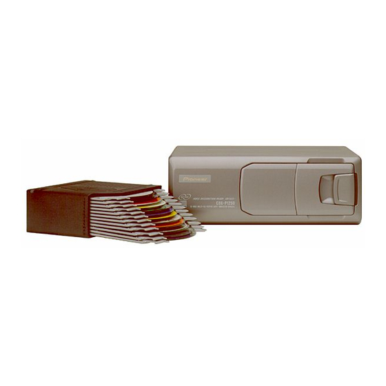
MULTI-COMPACT DISC PLAYER
CDX-P1250
CDX-P1250
CDX-P1250
- See the separate manual CX-938(CRT2357) for the CD mechanism description, disassembly and circuit
description.
- The CD mechanism employed in this model is one of C8 series.
CONTENTS
1. SAFETY INFORMATION ............................................3
2. EXPLODED VIEWS AND PARTS LIST .......................4
3. SCHEMATIC DIAGRAM ...........................................12
4. PCB CONNECTION DIAGRAM ................................20
5. ELECTRICAL PARTS LIST ........................................26
6. ADJUSTMENT..........................................................29
PIONEER ELECTRONIC CORPORATION
PIONEER ELECTRONICS SERVICE INC.
PIONEER ELECTRONIC [EUROPE] N.V.
PIONEER ELECTRONICS ASIACENTRE PTE.LTD. 253 Alexandra Road, #04-01, Singapore 159936
C PIONEER ELECTRONIC CORPORATION 1999
CDX-P1250/X1N/UC
X1N/EW
X1N/ES
4-1, Meguro 1-Chome, Meguro-ku, Tokyo 153-8654, Japan
P.O.Box 1760, Long Beach, CA 90801-1760 U.S.A.
Haven 1087 Keetberglaan 1, 9120 Melsele, Belgium
7. GENERAL INFORMATION .......................................35
7.1 IC .........................................................................35
7.2 DIAGNOSIS ........................................................40
7.2.1 DISASSEMBLY .........................................40
7.2.2 TEST MODE ..............................................42
7.3 BLOCK DIAGRAM ..............................................48
8. OPERATIONS AND SPECIFICATIONS.....................50
K-ZZY. FEB. 1999 Printed in Japan
ORDER NO.
CRT2318
X1N/UC
Advertisement
Table of Contents

Related Manuals for Pioneer CDX-P1250


Summary of Contents for Pioneer CDX-P1250
-
Page 1: Table Of Contents
PIONEER ELECTRONICS SERVICE INC. P.O.Box 1760, Long Beach, CA 90801-1760 U.S.A. PIONEER ELECTRONIC [EUROPE] N.V. Haven 1087 Keetberglaan 1, 9120 Melsele, Belgium PIONEER ELECTRONICS ASIACENTRE PTE.LTD. 253 Alexandra Road, #04-01, Singapore 159936 C PIONEER ELECTRONIC CORPORATION 1999 K-ZZY. FEB. 1999 Printed in Japan... - Page 2 CDX-P1250 - CD Player Service Precautions 3. Please checking the grating after changing the pickup 1. For pickup unit(CXX1285) handling, please refer unit(see page 29) since these screws protects the to"Disassembly"(See page 40). During replacement, mechanism during transport, be sure to affix it when handling precautions shall be taken to prevent an it is transported for repair, etc.
-
Page 3: Safety Information
CDX-P1250 1. SAFETY INFORMATION 1.1 CDX-P1250/X1N/UC CAUTION This service manual is intended for qualified service technicians; it is not meant for the casual do-it-yourselfer. Qualified technicians have the necessary test equipment and tools, and have been trained to properly and safely repair complex products such as those covered by this manual. -
Page 4: Exploded Views And Parts List
CDX-P1250 2. EXPLODED VIEWS AND PARTS LIST 2.1 PACKING... - Page 5 CDX-P1250 NOTE: - Parts marked by “*”are generally unavailable because they are not in our Master Spare Parts List. ∇ mark on the product are used for disassembly. - Screws adjacent to - PACKING SECTION PARTS LIST Part No. Mark No. Description...
- Page 6 CDX-P1250 2.2 EXTERIOR...
- Page 7 23 Lower Case Unit See Contrast table(2) 24 Grille Unit See Contrast table(2) 25 Screw BPZ20P080FMC (2) CONTRAST TABLE CDX-P1250/X1N/UC, CDX-P1250/X1N/EW and CDX-P1250/X1N/ES are constructed the same except for the following: Part No. Mark No. Symbol and Description CDX-P1250/X1N/UC CDX-P1250/X1N/EW CDX-P1250/X1N/ES...
- Page 8 CDX-P1250 2.3 CD MECHANISM MODULE...
- Page 9 CDX-P1250 (1)CD MECHANISM MODULE SECTION PARTS LIST Mark No. Description Part No. Mark No. Description Part No. 1 Connector CDE6069 46 Plate CNC8375 2 CD Core Unit(C8) 47 Cover CNC8434 See Contrast table(2) 3 Connector(CN701) CKS1953 48 Sheet CNM6009 4 Connector(CN101)
- Page 10 PT4800 CSN1051 Spring Switch(S851,S853) 103 LED(D851) CN504-2 104 Spring Switch(S852) CSN1052 (2) CONTRAST TABLE CDX-P1250/X1N/UC, CDX-P1250/X1N/EW and CDX-P1250/X1N/ES are constructed the same except for the following: Part No. Mark No. Symbol and Description CDX-P1250/X1N/UC CDX-P1250/X1N/EW CDX-P1250/X1N/ES 2 CD Core Unit(C8)
- Page 11 CDX-P1250 2.4 MAGAZINE ASSY - MAGAZINE ASSY SECTION PARTS LIST Mark No. Description Part No. 1 Magazine Assy CXB4028 2 Tray CNV5341 3 Label CRW1396...
-
Page 12: Schematic Diagram
CDX-P1250 3. SCHEMATIC DIAGRAM 3.1 OVERALL CONNECTION DIAGRAM Note: When ordering service parts, be sure to refer to “EXPLODED VIEWS AND PARTS LIST” or “ELECTRICAL PARTS LIST”. PICKUP UNIT(SERVICE) MECHANISM CXX1285 RF-A M854 CXB3004 M851 CXB3003 CSN1051 PT4800 SWITCH PCB... - Page 13 CDX-P1250 CD CORE UNIT EWmodel RF-AMP,SERVO, DSP,DAC UC,ES model 19 20 DRIVER MOTOR DRIVER A1/2...
- Page 14 CDX-P1250 SYSTEM CONTROLLER A2/2...
- Page 15 CDX-P1250 GGC1257 (SRM2B256SLTMX70) SRAM CN911 IP-BUS DRIVER A2/2...
- Page 16 CDX-P1250 Note:1. The encircled numbers denote measuring pointes in the circuit diagram. 2. Reference voltage REFO:2.5V - Waveforms 1 RFI 1 CH1: RFI 1 CH1: RFI 0.5V/div. 0.5µs/div. 1V/div. 1V/div. 0.5ms/div. 0.5ms/div. 2 CH2: MIRR 2 CH2: MIRR Normal mode: play 5V/div.
- Page 17 CDX-P1250 8 CH1: TE 8 CH1: TE 0 MD 0.2V/div. 0.5V/div. 0.5V/div. 0.1s/div. 20ms/div. 5ms/div. 9 CH2: TD ! CH2: SD 0.2V/div. 0.5V/div. Normal mode: play TEST mode:100Tracks jump(FWD) Normal mode: Play (12cm) → REFO → REFO → REFO →...
- Page 18 CDX-P1250 ( CH1: R OUT 6 CH1: FE 8 CH1: TE 2V/div. 0.2V/div. 0.2V/div. 500µs/div. 1ms/div. 1ms/div. ) CH2: L OUT 3 CH2: FD 9 CH2: TD 2V/div. 0.5V/div. 0.5V/div. Normal mode: Play (1kHz 0dB) Normal mode: During AGC Normal mode: During AGC →...
- Page 19 CDX-P1250 3.2 POWER UNIT...
-
Page 20: Pcb Connection Diagram
CDX-P1250 4. PCB CONNECTION DIAGRAM SIDE A M852 4.1 CD CORE UNIT NOTE FOR PCB DIAGRAMS 1. The parts mounted on this PCB include all necessary parts for several destination. For further information for respective destinations, be sure to check with the schematic dia-... - Page 21 CDX-P1250 2. Viewpoint of PCB diagrams SIDE B Capacitor Connector SIDE A SIDE B P.C.Board Chip Part...
- Page 22 CDX-P1250 4.2 POWER UNIT IP-BUS SIDE A POWER UNIT CORD CN701...
- Page 23 CDX-P1250 SIDE B POWER UNIT...
- Page 24 CDX-P1250 4.3 MECHANISM PCB MECHANISM PCB PICKUP UNIT M851 (SERVICE) SPDL HOME M854 CN101 4.4 SWITCH PCB SWITCH PCB D851...
- Page 25 CDX-P1250 4.5 MOTOR PCB MOTOR PCB...
-
Page 26: Electrical Parts List
CKS.., CCS.., CSZS..=====Circuit Symbol and No.===Part Name Part No. =====Circuit Symbol and No.===Part Name Part No. ------ ------------------------------------------ ------------------------- ------ ------------------------------------------ ------------------------- Unit Number : CWX2262(CDX-P1250/X1N/UC,ES) RS1/16S102J CWX2263(CDX-P1250/X1N/EW) RS1/16S681J Unit Name : CD Core Unit RS1/16S681J RS1/16S103J MISCELLANEOUS RS1/16S153J UPD63710GC... - Page 27 CDX-P1250 =====Circuit Symbol and No.===Part Name Part No. =====Circuit Symbol and No.===Part Name Part No. ------ ------------------------------------------ ------------------------- ------ ------------------------------------------ ------------------------- RS1/16S222J CKSQYB224K16 RS1/16S683J (EW model) CKSQYB104K25 RS1/16S222J (EW model) CKSRYB471K50 RS1/16S473J CCSRCH391J50 RS1/16S222J CCSRCH391J50 RS1/16S103J CCSRCH181J50 RS1/16S433J CCSRCH181J50 RS1/16S104J...
- Page 28 CDX-P1250 =====Circuit Symbol and No.===Part Name Part No. ------ ------------------------------------------ ------------------------- RS1/10S362J RS1/10S222J CAPACITORS CKSQYB104K50 470µF/16V CCH1183 CKSQYB223K25 470µF/16V CCH1183 0.22F/5.5V CCL1037 CKSQYB103K50 CKSQYB103K50 CEJA220M10 CKSQYB103K50 CEJA330M10 CEJA330M10 Unit Number Unit Name : Mechanism PCB Photo-transistor PT4800 Spring Switch(HOME) CSN1051...
-
Page 29: Adjustment
CDX-P1250 6. ADJUSTMENT 6.1 CHECKING THE GRATING - Checking the Grating After Changing the Pickup Unit • Note : CD mechanism modules the grating angle of the pickup unit cannot be adjusted after the pickup unit is changed. The pickup unit in the CD mechanism module is adjusted on the production line to match the CD mechanism module and is thus the best adjusted pickup unit for the CD mechanism module. - Page 30 CDX-P1250 Grating waveform Echt Xch 20mV/div, AC Fcht Ych 20mV/div, AC 0˚ 30˚ 45˚ 60˚ 75˚ 90˚...
- Page 31 CDX-P1250 6.2 ADJUSTMENT OF ELEVATION WHEN THE CD CORE UNIT HAS BEEN REMOVED FOR MAINTENANCE - Adjustment When Error Code 60 is Displayed Because of Malfunctioning Elevation • Note : This mechanisms is detects the height of the stage using slide-variable resistance.
- Page 32 CDX-P1250 Examples of display 4. Press key 9 to set ELV/TRAY mode to TRAY. TRACK FUNCTION 01' 02" 5. Press key FF to release the clamp and return the tray to the magazine. Release the clamp 6. Press key 9 to enter Elevation Move mode.
- Page 33 CDX-P1250 12. To see the amount of dislocation, place the mechanism upside-down. If the stopper bend has been dislocated in the direction of the first VR802 CD, turn VR802 to the left(Fig. 2). EREF To lower the stage toward the twelfth step by 0.1 mm, reduce the voltage of EREF (adjusted in step 8) by 10 mV.
- Page 34 CDX-P1250 Stopper bend of the clamp lever Frame stopper Dislocated toward the first CD. Fig. 2 Adjust the insertion gate of magazine to the sixth scale. Fig. 1 Engaged in the center and pressed downward. Fig. 3 Dislocated toward the twelfth CD.
-
Page 35: General Information
CDX-P1250 7. GENERAL INFORMATION 7.1 IC - Pin Functions (UPD63710GC) Pin No. Pin Name Function and Operation Logic circuit GND HOLD Defect detection output MIRR MIRR output RFOK signal output Reset signal input Command/parameter identification signal input Data strobe signal input... - Page 36 CDX-P1250 Pin No. Pin Name Function and Operation PACK CD-TEXT PACK synchronous signal CD-TEXT data serial output CD-TEXT control parameter serial input tsck CD-TEXT serial clock input TSTB CD-TEXT parameter strobe signal input Logic circuit GND TEST Test pin ATEST...
- Page 37 CDX-P1250 *UPD63710GC IC's marked by* are MOS type. Be careful in handling them because they are very liable to be damaged by electrostatic induction. BA05FP Reference voltage BA5986FM Mute Level shift Level shift Level shift Level shift Stand-by...
- Page 38 CDX-P1250 - Pin Functions (PD5513A) Pin No. Pin Name Format Function and Operation Not used adena A/D reference voltage output TXTSTE TEXT parameter output TXTSO TEXT control parameter serial output TXTSI TEXT data serial input TXTSCK TEXT clock output BYTE...
- Page 39 CDX-P1250 Pin No. Pin Name Format Function and Operation 65–68 A6-A3 SRAM address bus output SRAM address bus output A2 & (EPSK) SRAM address bus output and (E2PROM clock output) A1 & (EPDI) SRAM address bus output and (E2PROM data input) A0 &...
-
Page 40: Diagnosis
CDX-P1250 7.2 DIAGNOSIS 7.2.1 DISASSEMBLY CD Mechanism Module Removing the Upper Case(not shown) 1. Remove the night screws. 2. Remove the Upper Case. Removing the CD Mechanism Module Remove the four dampers(Fig.5). Disconnect the connector(Fig.5). Remove the two springs(Fig.5). Fig.5 Disconnect the connector and then remove the CD Mechanism Module(Fig.6). - Page 41 CDX-P1250 - Removing the Pickup Unit 1. Insert the short pin from the pickup unit in the flexible substrate. 2. Remove the flexible substrate from the connector. 3. Remove the flexible card from the connector. 4. Remove the lead wires to which the spindle motor and carriage motor assy were soldered.
-
Page 42: Test Mode
CDX-P1250 7.2.2 TEST MODE - CD Test Mode 1) Precautions 2) Test Mode • This unit uses a single power supply (+5V) for the reg- This mode is used for adjusting the CD mechanism ulator. The signal reference potential, therefore, is module of the device. - Page 43 CDX-P1250 - Flow Chart Test Mode In Reset SOURCE Sourse CD New test mode BAND Power ON (Adjustment for T.Offset) Power ON RF AMP Gain Select (Not adjustment for T.Offset) 00 00 00 Display 99 99 99 GG GG GG...
- Page 44 CDX-P1250 - Error Messages If a CD is not operative or stopped during operation due to an error, the error mode is turned on and cause(s) of the error is indicated with a corresponding number. This arrangement is intended at reducing nonsense calls from the users and also for facilitating trouble analysis and repair work in servicing.
- Page 45 CDX-P1250 Code Class Displayed error code Description of the code and potential cause(s) Mecha- An error upon Elevation time has time out. nism elevation Mecha- An error with an em- No disc is available. nism pty magazine inserted Remarks: Unreadable TOC does not constitute an error. An intended operation continues in this case.
- Page 46 CDX-P1250 Mechanism Test Mode (Example) BAND Back to the test mode Playing the mechanism DOWN Playing the mechanism Mechanism test mode in – TRAY/ELV select – – Operation step select Note: Eject and CD on/off is performed in the same procedure as that for the normal mode.
- Page 47 CDX-P1250 Status No. Contents Protective action Focus search preprocessing is in None progress while focus recovery is turned on. Wait time after focus close is set up. Off focus. Standing by after focus close is over. Off focus. Setup (1/2) before T balance adjustment is started.
-
Page 48: Block Diagram
CDX-P1250 7.3 BLOCK DIAGRAM... - Page 49 CDX-P1250...
-
Page 50: Operations And Specifications
CDX-P1250 8. OPERATIONS AND SPECIFICATIONS 8.1 OPERATION If the power does not switch on or if the compact disc player does not operate when the button on the multi-CD controller is pressed, or if the multi-CD controller display is incorrect, press this button on the player with the tip of a pencil to restore normal operation.
Need help?
Do you have a question about the CDX-P1250 and is the answer not in the manual?
Questions and answers