Sony DVP-S335 Service Manual
Cd/dvd player
Hide thumbs
Also See for DVP-S335:
- Service manual (113 pages) ,
- Operating instructions manual (72 pages) ,
- Service manual (113 pages)
Table of Contents
Advertisement
SERVICE MANUAL
CD/DVD player
Laser
Semiconductor laser
Signal format system
PAL/(NTSC)
Audio characteristics
Frequency response
DVD (PCM 96 kHz): 2 Hz to 44 kHz
(±1 dB)*
DVD (PCM 48 kHz): 2 Hz to 22 kHz
(±0.5 dB)
CD: 2 Hz to 20 kHz (±0.5 dB)
Signal-to-noise ratio
More than 110 dB (AUDIO OUT connectors
only) (EXCEPT S735D: E, EA, AUS)
More than 115 dB (AUDIO OUT
only) (S735D: E, EA, AUS)
Harmonic distortion
Less than 0.003 % (EXCEPT S735D)
Less than 0.0025 % (S735D)
Dynamic range
More than 100 dB (DVD)
More than 97 dB (CD) (EXCEPT S735D)
More than 98 dB (CD) (S735D)
Wow and flutter
Less than detected value
(±0.001 % W PEAK)
DVP-S335/S336/S345/
RMT-D115E/D115P/D116P/D120E/D120O/D120P
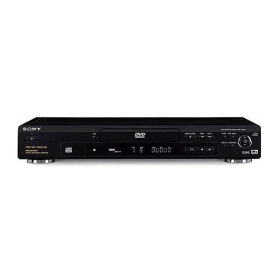
Photo: DVP-S335
SPECIFICATIONS
AUDIO OUT
DIGITAL OUT
(OPTICAL)
DIGITAL OUT
(COAXIAL)
VIDEO OUT
S VIDEO OUT
connectors
5.1CH
OUTPUT
(S535D/S735D)
PHONES
(S535D/S735D)
COMPONENT
VIDEO OUT
(Y, C
C
(S335: E, EA/
S336: AUS/
S345/S735D)
AUDIO OUT
(WOOFER)
(S335/S336/
S345)
S535D/S735D
DVP-S335/S336/S535D/S735D
Saudi Arabia Model
Australian Model
Outputs
Jack
Output
type
level
Phono
2 Vrms
jacks
(at 50 kilohms)
Optical
–18 dBm
output
connector
Phono
0.5 Vp-p
jack
Phono
1.0 Vp-p
jacks
4-pin
Y: 1.0 Vp-p
mini DIN
C: 0.3 Vp-p
(PAL)
C: 0.286 Vp-p
(NTSC)
Phono
2 Vrms
jack
(at 50 kilohms)
Phone
12 mW
jack
Phono
Y: 1.0 Vp-p
jacks
/B-Y,
B
/R-Y)
C
/B-Y ,
B
R
C
/R-Y :
R
0.7 Vp-p
Phono
2 Vrms
jack
(at 50 kilohms)
AEP Model
UK Model
Russian Model
DVP-S335/S735D
E Model
DVP-S335/S345/S735D
DVP-S336/S735D
Load impedance
Over 10 kilohms
Wave length: 660 nm
75 ohms terminated
75 ohms,
sync negative
75 ohms,
sync negative
75 ohms terminated
Over 10 kilohms
32 ohms
75 ohms,
sync negative
75 ohms
Over 10 kilohms
– Continued on next page –
CD/DVD PLAYER
Advertisement
Table of Contents

Related Manuals for Sony DVP-S335


Summary of Contents for Sony DVP-S335
- Page 1 S535D/S735D RMT-D115E/D115P/D116P/D120E/D120O/D120P SERVICE MANUAL AEP Model UK Model DVP-S335/S336/S535D/S735D Russian Model Saudi Arabia Model DVP-S335/S735D E Model DVP-S335/S345/S735D Australian Model DVP-S336/S735D Photo: DVP-S335 SPECIFICATIONS CD/DVD player Outputs Laser Semiconductor laser Signal format system Jack Output Load impedance PAL/(NTSC) type level...
- Page 2 LINE WITH MARK 0 ON THE SCHEMATIC DIAGRAMS AND IN THE PARTS LIST ARE CRITICAL TO SAFE OPERATION. REPLACE THESE COMPONENTS WITH SONY PARTS WHOSE PART NUMBERS APPEAR AS SHOWN IN THIS MANUAL OR IN SUPPLEMENTS PUB- LISHED BY SONY.
-
Page 3: Table Of Contents
TABLE OF CONTENTS Section Title Page Section Title Page Service Note ................4 HS16S9E Printed Wiring Board ........4-59 HS16S9E Schematic Diagram ........4-61 GENERAL IC PIN FUNCTION DESCRIPTION Getting Started .............. 1-1 Playing Discs ..............1-4 5-1. System Control Pin Function Using Various Functions with the Control Menu ... -
Page 4: Service Note
SERVICE NOTE 1. DISASSEMBLY • This set can be disassembled in the order shown below. Case (Page 2-1) Rear Panel Tray Cover (Page 2-1) (Page 2-1) Mechanism Front Panel Deck (Page 2-1) (Page 2-2) Power AI-17 Board Tray MB-86 Board Block (Page 2-2) (Page 2-3) - Page 5 2. DISC REMOVAL PROCEDURE 3. HOW TO SERVICE MB-86 BOARD (at POWER OFF) 1) Remove the case from the set. (Refer to 2-1) 2) Remove the mechanism deck. (Refer to 2-6) 1) Insert a tapering driver into the aperture of the unit bottom, 3) Remove the MB-86 board.
- Page 6 6) Set the CK-MB board as shown in Fig. 4. 8) Set the mechanism deck as shown in Fig. 6. 1 MB-86 board 3 CK-MB board MB-86 board 2 Two connectors (CN101, 102) Mechanism deck Fig. 4 Fig. 6 7) Set the CK-AI board as shown in Fig. 5. 5 Connector (CN103) 7 Flexible board...
-
Page 7: General
DVP-S335/S336/S345/S535D/S735D SECTION 1 This section is extracted from DVP-S335/ GENERAL S336 instruction manual (3-059-581-11). - Page 16 1-10...
- Page 17 1-11...
- Page 18 1-12...
- Page 19 1-13...
- Page 20 1-14...
- Page 21 1-15 E 1-15...
-
Page 22: Disassembly
DVP-S335/S336/S345/S535D/S735D SECTION 2 DISASSEMBLY Note: Follow the disassembly procedure in the numerical order given. 2-1. CASE REMOVAL 2-3. TRAY COVER REMOVAL 3 Two claws 4 Case 3 Screw 1 Two screws 4 Tray cover 2 Pull the tray in the 2 Two direction of arrow B. -
Page 23: Power Block Removal
2-5. POWER BLOCK REMOVAL 2-7. TRAY REMOVAL 1 Two screws 1 Connector (BTP2.6 × 12) (CN101) 2 Chuck holder 4 Two ground point screws 3 Two screws (B3) 6 Power block 2 Connector (CN201) 4 Remove the tray in the direction of arrow B. -
Page 24: Belt, Mb-86 Board, Loading Motor (M001)
2-9. BELT, MB-86 BOARD, LOADING MOTOR (M001), MS-48 BOARD REMOVAL 1 Belt 2 Two screws (B2.6 × 4) 4 Claw 7 MB-86 board 5 Flexible board 6 Flexible board (CN201) (CN401) 8 Three claws 3 Flexible board 9 Loading motor (M001), (CN202) MS-48 board 2-10. -
Page 25: Internal Views
2-11. INTERNAL VIEWS Optical pick-up (KHM-220AAA/J1RP) Lever switch A-6062-397-A 1-771-562-11 DC motor (loading) 1-541-632-11 Flexible flat cable 1-792-457-11 DC motor (loading) 1-541-632-11... -
Page 26: Circuit Boards Location
2-12. CIRCUIT BOARDS LOCATION ER-9 S335: AEP, UK, RU/S336: AEP, UK/ Power Block (HS16S9E) S535D/S735D: AEP, UK, RU (SWITCHING REGULATOR) (EURO AV) MB-86 (SIGNAL PROCESS, SERVO) HP-127 (S535D/S735D) (HEADPHONE) AI-17 MS-48 AUDIO, VIDEO BUFFER, (LOADING) FUNCTION SWITCH 2-5 E... -
Page 27: Block Diagrams
DVP-S335/S336/S345/S535D/S735D SECTION 3 BLOCK DIAGRAMS 3-1. OVERALL BLOCK DIAGRAM AI-17 BOARD MB-86 BOARD S535D/S735D (SEE PAGE 4-35 to 4-46) (SEE PAGE 4-11 to 4-32) IC303 IC504, 505 IC601 VIDEO Y, S335: E, EA/ VIDEO B – Y, 16M DRAM 16M SDRAM S336: AUS/ VIDEO R –Y... -
Page 28: Rf/Servo Block Diagram
DVP-S335/S336/S345/S535D/S735D 3-2. RF/SERVO BLOCK DIAGRAM IC201 tf (CD play) IC201 1 (DVD play) IC201 1 (CD play) IC201 tf (DVD play) IC201 r; (DVD play) IC201 r; (CD play) 500 mV/DIV 500 ns/DIV 200 mV/DIV 100 ns/DIV 500 mV/DIV 500 ns/DIV... -
Page 29: Signal Processor Block Diagram
DVP-S335/S336/S345/S535D/S735D 3-3. SIGNAL PROCESSOR BLOCK DIAGRAM MB-86 BOARD (2/6) (SEE PAGE 4-13 to 4-20) IC303 IC504, 505 16M DRAM 16M SDRAM IC302 qj (DVD play) 500 mV/DIV 100 ns/DIV IC502 yl (RGB output) IC502 yl 136 – 139 154 – 157 124 125 127 128 157 –... -
Page 30: System Control Block Diagram
DVP-S335/S336/S345/S535D/S735D 3-4. SYSTEM CONTROL BLOCK DIAGRAM MB-86 BOARD (3/6) (SEE PAGE 4-25 to 4-32) IC104 IC802 FLASH NAND FLASH HD 8 – 15 HD 8 – 15 RF/SERVO (SEE PAGE 3-4) HA 0, 1 HA 0, 1 HA 0 – 21 HA 0 –... -
Page 31: Audio (1) Block Diagram
DVP-S335/S336/S345/S535D/S735D 3-5. AUDIO (1) BLOCK DIAGRAM IC101 wg AI-17 BOARD (2/3) MB-86 BOARD (5/6) IC101 (SEE PAGE 4-35, 37) (SEE PAGE 4-15) VIDEO BUFFER S335: E, EA/ • Abbreviation J101 CN101 (1/2) CN501 S336: AUS/ 1.0 Vp-p (H) : Australian... -
Page 32: Video/Audio (2) Block Diagram
DVP-S335/S336/S345/S535D/S735D 3-6. VIDEO/AUDIO (2) BLOCK DIAGRAM MB-86 BOARD (4/6) J303 AI-17 BOARD (1/3) (SEE PAGE 4-31) (SEE PAGE 4-37 to 4-44) COAXIAL DIGITAL Q312 – 314 IC306 1 D IN CN701 (1/2) CN201 (1/2) OPTICAL SPDIF SPDIF S535D/S735D S535D/S735D IC303... -
Page 33: Interface Control Block Diagram
DVP-S335/S336/S345/S535D/S735D 3-7. INTERFACE CONTROL BLOCK DIAGRAM MB-86 BOARD (6/6) AI-17 BOARD (3/3) (SEE PAGE 4-31) (SEE PAGE 4-37, 41 to 4-46) CN701 (1/2) CN201 (2/2) BZ401 BUZZER HP-127 BOARD (2/2) IC401 (SEE PAGE 4-57) REMOTE COMMANDER CN404 RECEIVER CN501 S335/S336/S345... -
Page 34: Power Block Diagram
DVP-S335/S336/S345/S535D/S735D 3-8. POWER BLOCK DIAGRAM S535D/S735D AI-17 BOARD (SEE PAGE 4-35 to 4-46) HP-127 BOARD HS16S9E BOARD T101 P611 CN201 CN401 (SEE PAGE 4-57) (SEE PAGE 4-61) EVER +3V EVER +3V IC403 CN404 CN501 EVER +5V EVER +5V IC501 SW101... -
Page 35: Printed Wiring Boards And Schematic Diagrams
DVP-S335/S336/S345/S535D/S735D DVP-S335/S336/S345/S535D/S735D SECTION 4 PRINTED WIRING BOARDS AND SCHEMATIC DIAGRAMS THIS NOTE IS COMMON FOR PRINTED WIRING For schematic Diagram: • Caution when replacing chip parts. BOARDS AND SCHEMATIC DIAGRAMS. New parts must be attached after removal of chip. (In addition to this, the necessary mote is printed Be careful not to heat the minus side of tantalum capacitor, in each block.) -
Page 36: Frame Schematic Diagrams
DVP-S335/S336/S345/S535D/S735D 4-1. FRAME SCHEMATIC DIAGRAM S535D/S735D CN201 CN101 CN401 DOWN LOAD(JIG) AC_IN(L) EVER+3.8V EVER+3.8V CN403 AC_IN(N) SW+3.3V SW+3.3V XFRRST SW+3.3V SW+3.3V XIFBUSY CN404 CN501 EVER+5.6V EVER+5.6V XIFCS EVER+5V EVER+5V D_GND D_GND SIRCS SIRCS D_GND D_GND BtoB SW+10V SW+10V HP-V HP-V... -
Page 37: Printed Wiring Boards And Schematic Diagrams
DVP-S335/S336/S345/S535D/S735D 4-2. PRINTED WIRING BOARDS AND SCHEMATIC DIAGRAMS MS-48 (LOADING) PRINTED WIRING BOARD AND SCHEMATIC DIAGRAM – Ref. No.: MS-48 board; 2,000 series – MS-48 BOARD There are few cases that the part isn't mounted in this model is printed on this diagram. - Page 38 DVP-S335/S336/S345/S535D/S735D There are few cases that the part isn't mounted in this model is printed on this diagram. MB-86 (SIGNAL PROCESS, SERVO) PRINTED WIRING BOARD – Ref. No.: MB-86 board; 1,000 series – MB-86 BOARD (SIDE A) CN102 CN201 CN401...
- Page 39 DVP-S335/S336/S345/S535D/S735D • Waveforms 1 IC201 1 (DVD play) 3 IC201 el (CD play) 200 mV/DIV 100 ns/DIV 500 mV/DIV 200 ms/DIV 536 mVp-p 1.7 Vp-p 1 IC201 1 (CD play) 4 IC201 r; (DVD play) 500 mV/DIV 500 ns/DIV 100 mV/DIV 50 ms/DIV...
-
Page 40: Rf Amp, Servo) Schematic Diagram
DVP-S335/S336/S345/S535D/S735D MB-86 (RF AMP, SERVO) SCHEMATIC DIAGRAM • See page 4-7 for printed wiring board and page 4-10 for waveforms. – Ref. No.: MB-86 board; 1,000 series – MB-86 BOARD (1/11) CN201 N.C. JL201 JL202 C233 DVD/CD C228 MB-86 BOARD (3/11) -
Page 41: Arp) Schematic Diagram
DVP-S335/S336/S345/S535D/S735D MB-86 (ARP) SCHEMATIC DIAGRAM • See page 4-7 for printed wiring board. – Ref. No.: MB-86 board; 1,000 series – MB-86 BOARD (2/11) FL303 +3.3V MB-86 BOARD (3/11) D_GND C319 100u 6.3V JL312 IC303 C302 IC301 100u 16M DRAM... -
Page 42: Av Decoder) Schematic Diagram
DVP-S335/S336/S345/S535D/S735D MB-86 (AV DECODER) SCHEMATIC DIAGRAM • See page 4-7 for printed wiring board. – Ref. No.: MB-86 board; 1,000 series – MB-86 BOARD (3/11) AVINT AVWT MB-86 BOARD (8/11) DACK0 XAVDCS3 DREQ0 MB-86 BOARD (8/11) XAVDCS2 DACK1 R517 27MAVD... -
Page 43: Sdram) Schematic Diagram
DVP-S335/S336/S345/S535D/S735D MB-86 (SDRAM) SCHEMATIC DIAGRAM • See page 4-7 for printed wiring board. • Waveforms – Ref. No.: MB-86 board; 1,000 series – 3 IC502 yl (RGB output) 1 IC502 yd MB-86 BOARD (4/11) IC504 16M SDRAM 720 mVp-p (H) 1.0 Vp-p (H) -
Page 44: Vga) Schematic Diagram
DVP-S335/S336/S345/S535D/S735D MB-86 (VGA) SCHEMATIC DIAGRAM • See page 4-7 for printed wiring board. – Ref. No.: MB-86 board; 1,000 series – MB-86 BOARD (5/11) S535D/S735D PDO0 PDO0 C602 PDO1 0.01u PDO1 PDO2 PDO2 PDO3 PDO3 PDO4 PDO4 PDO5 PDO5 PDO6... -
Page 45: Drive) Schematic Diagram
DVP-S335/S336/S345/S535D/S735D MB-86 (DRIVE) SCHEMATIC DIAGRAM • See page 4-7 for printed wiring board. – Ref. No.: MB-86 board; 1,000 series – MB-86 BOARD (6/11) NO MARK:DVD/CD PLAY D:DVD PLAY C:CD PLAY JL428 MB-86 BOARD (1/11) TIA+ R423 R436 C407 R407 0.1u... -
Page 46: Servo Dsp) Schematic Diagram
DVP-S335/S336/S345/S535D/S735D MB-86 (SERVO DSP) SCHEMATIC DIAGRAM • See page 4-7 for printed wiring board. – Ref. No.: MB-86 board; 1,000 series – • Waveforms 1 IC404 ws (DVD play) MB-86 BOARD (7/11) 100 mV/DIV 50 ms/DIV NO MARK:DVD/CD PLAY D:DVD PLAY... -
Page 47: System Control) Schematic Diagram
DVP-S335/S336/S345/S535D/S735D MB-86 (SYSTEM CONTROL) SCHEMATIC DIAGRAM • See page 4-7 for printed wiring board. – Ref. No.: MB-86 board; 1,000 series – MB-86 BOARD (8/11) R126 NO MARK:DVD/CD PLAY R124 220k :S735D D:DVD PLAY 4.7k:S336:AUS/S735D:AUS 470k :S535D 8.2k :S335:E,EA/S735D:EA C:CD PLAY... -
Page 48: Memory, Clock Generator) Schematic Diagram
DVP-S335/S336/S345/S535D/S735D MB-86 (MEMORY, CLOCK GENERATOR) SCHEMATIC DIAGRAM • See page 4-7 for printed wiring board. – Ref. No.: MB-86 board; 1,000 series – MB-86 BOARD (9/11) NO MARK:DVD/CD PLAY D:DVD PLAY C:CD PLAY R105 27MAVD MB-86 BOARD(3/11) FB104 FB102 R139... -
Page 49: Mb-86 (Fga) Schematic Diagram
DVP-S335/S336/S345/S535D/S735D MB-86 (FGA) SCHEMATIC DIAGRAM • See page 4-7 for printed wiring board. – Ref. No.: MB-86 board; 1,000 series – MB-86 BOARD (10/11) NO MARK:DVD/CD PLAY D:DVD PLAY C:CD PLAY *:IMPOSSIBLE TO MEASURE THE VOLTAGE AT THE MARKED POINTS. -
Page 50: Audio Dsp) Schematic Diagram
DVP-S335/S336/S345/S535D/S735D MB-86 (AUDIO DSP) SCHEMATIC DIAGRAM • See page 4-7 for printed wiring board. – Ref. No.: MB-86 board; 1,000 series – MB-86 BOARD (11/11) NO MARK:DVD/CD PLAY D:DVD PLAY S335/S336/S345 C:CD PLAY LRCK ACH12 MB-86 BOARD (3/11) ACH34 ACH56... -
Page 51: Printed Wiring Board
DVP-S335/S336/S345/S535D/S735D AI-17 (AUDIO, VIDEO BUFFER, FUNCTION SWITCH) PRINTED WIRING BOARD – Ref. No.: AI-17 board; 2,000 series – There are few cases that the part isn't mounted in this model is printed on this diagram. ER-9 S335: AEP, UK, RU/S336: AEP, UK/... -
Page 52: Video Buffer) Schematic Diagram
DVP-S335/S336/S345/S535D/S735D AI-17 (VIDEO BUFFER) SCHEMATIC DIAGRAM • See page 4-33 for printed wiring board. – Ref. No.: AI-17 board; 2,000 series – AI-17 BOARD (1/6) NO MARK:DVD/CD PLAY IC101 MB-86 BOARD (3/11) VIDEO BUFFER *R114 CN501 :S335:AEP,UK,RU/S336:AEP,UK/S535D/S735D:AEP,UK,RU (SEE PAGE 4-15) -
Page 53: D/A Converter, Dsp) Schematic Diagram
DVP-S335/S336/S345/S535D/S735D AI-17 (D/A CONVERTER, DSP) SCHEMATIC DIAGRAM • See page 4-33 for printed wiring board. – Ref. No.: AI-17 board; 2,000 series – AI-17 BOARD (2/6) NO MARK:DVD/CD PLAY D:DVD PLAY C:CD PLAY S335/S336/S345 ERAUDIOR S335:AEP,UK,RU/S336:AEP,UK/S535D AI-17 BOARD (3/6) S735D:AEP,UK,RU... -
Page 54: Amp, Lpf) Schematic Diagram
DVP-S335/S336/S345/S535D/S735D AI-17 (AMP, LPF) SCHEMATIC DIAGRAM • See page 4-33 for printed wiring board. – Ref. No.: AI-17 board; 2,000 series – S535D/S735D R284,289 R286,291 :S535D :S535D :S735D :S735D AI-17 BOARD (3/6) HP_L R295 AI-17 BOARD (5/6) HP_GND Q213 R263 2SD1938(F)-T(TX).SO... -
Page 55: D/A Converter) Schematic Diagram
DVP-S335/S336/S345/S535D/S735D AI-17 (D/A CONVERTER) SCHEMATIC DIAGRAM • See page 4-33 for printed wiring board. – Ref. No.: AI-17 board; 2,000 series – AI-17 BOARD (4/6) R326 3300 C321 R360 820p 3900 C330 C336 R341 R347 C327 0.01u R327 3900 1800... -
Page 56: Mode Control, Power Supply
DVP-S335/S336/S345/S535D/S735D AI-17 (MODE CONTROL, POWER SUPPLY) SCHEMATIC DIAGRAM • See page 4-33 for printed wiring board. – Ref. No.: AI-17 board; 2,000 series – AI-17 BOARD (5/6) IC407 IC406 NO MARK:DVD/CD PLAY +3.3V REG +5V REG IC407 IC406 AN77033SP-(E1) PQ05DZ5U... -
Page 57: If Con) Schematic Diagram
DVP-S335/S336/S345/S535D/S735D AI-17 (IF CON) SCHEMATIC DIAGRAM – Ref. No.: AI-17 board; 2,000 series – AI-17 BOARD (6/6) R464 PCONT AI-17 BOARD (5/6) R462 R461 R460 R459 XIFCS AI-17 BOARD (2/6) R463 R608 XIFBUSY XFRRST S535D S735D C423 0.01u R453 AI-17 BOARD (5/6) - Page 58 There are few cases that the part isn't mounted in this model is printed on this diagram. – Ref. No.: ER-9 board; 2,000 series – – DVP-S335: AEP, UK, RU/S336: AEP, UK/S535D/S735D: AEP, UK, RU – ER-9 BOARD (SIDE A)
- Page 59 DVP-S335/S336/S345/S535D/S735D ER-9 BOARD (SIDE B) D902 D903 D904 D905 D906 D907 D908 D909 D911 D915 D918 D919 D920 D921 D922 D923 D926 D927 D931 IC902 IC903 Q904 Q909 Q911 Q912 Q913 Q914 Q915 Q916 Q917 EURO AV ER-9 4-49 4-50...
-
Page 60: Er-9 (Euro Av1) Schematic Diagram
DVP-S335/S336/S345/S535D/S735D ER-9 (EURO AV1) SCHEMATIC DIAGRAM • See page 4-47 for printed wiring board. – Ref. No.: ER-9 board; 2,000 series – – DVP-S335: AEP, UK, RU/S336: AEP, UK/S535D/S735D: AEP, UK, RU – ER-9 BOARD (1/2) NO MARK:DVD/CD PLAY IC901... -
Page 61: Euro Av2) Schematic Diagram
DVP-S335/S336/S345/S535D/S735D ER-9 (EURO AV2) SCHEMATIC DIAGRAM • See page 4-47 for printed wiring board. – Ref. No.: ER-9 board; 2,000 series – – DVP-S335: AEP, UK, RU/S336: AEP, UK/S535D/S735D: AEP, UK, RU – ER-9 BOARD (2/2) NO MARK:DVD/CD PLAY R927... - Page 62 DVP-S335/S336/S345/S535D/S735D DVP-S335/S336/S345/S535D/S735D HP-127 (HEADPHONE) PRINTED WIRING BOARD – Ref. No.: HP-127 board; 2,000 series – – DVP-S535D/S735D – There are few cases that the part isn't mounted in this model is printed on this diagram. HP-127 BOARD ER-9 S335: AEP, UK, RU/S336: AEP, UK/...
- Page 63 DVP-S335/S336/S345/S535D/S735D HP-127 (HEADPHONE) SCHEMATIC DIAGRAM – Ref. No.: HP-127 board; 2,000 series – – DVP-S535D/S735D – HP-127 BOARD IC501 NO MARK:DVD/CD PLAY GP1U28Y IC501 REMOTE COMMANDER RECEIVER R514 C504 C503 0.01u R513 R515 150k RV501 R509 LEVEL MIN/MAX D506 HZM6.8ZWA1TL...
-
Page 64: Hs16S9E Printed Wiring Board
DVP-S335/S336/S345/S535D/S735D HS16S9E (SWITCHING REGULATOR) PRINTED WIRING BOARD There are few cases that the part isn't mounted in this model is printed on this diagram. – Ref. No.:HS16S9E board; 3,000 series – HS16S9E BOARD CN101 CN201 D101 D102 D104 D105 D211... -
Page 65: Hs16S9E Schematic Diagram
DVP-S335/S336/S345/S535D/S735D HS16S9E (SWITCHING REGULATOR) SCHEMATIC DIAGRAM – Ref. No.: HS16S9E board; 3,000 series – HS16S9E BOARD L211 T101 D211 S2L20U 10uH 10.2 10.2 Q211 R211 2SJ525 SWITCH R105 C211 C213 R213 330uF 47uF 1/2W R212 CN201 13P EVER +3.8V L151 SW +3.3V... -
Page 66: Ic Pin Function Description
DVP-S335/S336/S345/S535D/S735D SECTION 5 IC PIN FUNCTION DESCRIPTION... - Page 67 5-2 E...
-
Page 68: Test Mode
DVP-S335/S336/S345/S535D/S735D SECTION 6 TEST MODE 6-1. GENERAL DESCRIPTION ### Syscon Diagnosis ### Diag All Check The Test Mode allows you to make diagnosis and adjustment eas- No. 2 Version ily using the remote commander and monitor TV. The instructions, diagnostic results, etc. are given on the on-screen display (OSD). - Page 69 Error 12: Read data discord ber. (4-3) DSP Driver Test Test signal data → DSP Driver Model Type Error: Not detected. DVP-S335 (AEP50, UK) DVP-S335 (AEP51) 5. Supply DVC-S335 (RU) Caution: Do not conduct this check with a mechanical deck con- nected.
- Page 70 Before starting the test, all addresses of RAM (IC303) are 6. AV Decoder cleared to 0x0000. (6-2) 1930 RAM Data write → read, and accord check First, 0xA55A is written to the address 0x00000, and the address data are read and checked from addresses 0x00001 Error 13: AVD RAM read data discord to 0x80000 while shifting 1 bit each.
- Page 71 8. Audio Error Codes List (8-2) ARP → 1930 00: Error not detected Error 14 : ARP → 1930 video NG 01: RAM write/read data discord 15 : ARP → 1930 audio NG 02: Gate array NG 03: EEPROM NG 04: Flash memory clear error (8-3) Test Tone 05: Flash memory write error...
-
Page 72: Drive Auto Adjustment
6-4. DRIVE AUTO ADJUSTMENT 1. DVD-SL (single layer) [ENTER] Select , insert DVD single layer disc, and press key, and the adjustment will be made through the following steps, then On the Test Mode Menu screen, press key on the remote com- adjusted values will be written to the EEPROM. - Page 73 2. CD 3. DVD-DL (dual layer) [ENTER] [ENTER] Select , insert CD disc, and press key, and the adjust- Select , insert DVD dual layer disc, and press key, ment will be made through the following steps, then adjusted val- and the adjustment will be made through the following steps, then ues will be written to the EEPROM.
-
Page 74: Drive Manual Operation
4. SACD 6-5. DRIVE MANUAL OPERATION [ENTER] Select , insert SACD disc, and press key, and the adjustment will be made through the following steps, then adjusted On the Test Mode Menu screen, select , and the manual opera- values will be written to the EEPROM. However, if SACD disc is tion menu will be displayed. - Page 75 0. Disc Check Memory Disc Type 1. Disc Type Auto Check Disc Check 2. DVD SL 12 cm 3. DVD DL 12 cm 4. CD 12cm 5. SACD 12 cm 1. SL Disc Check 6. DVD SL 8 cm 2. CD Disc Check 7.
-
Page 76: Mecha Aging
Reset SLED TILT Reset the Sled and Tilt to initial posi- 6-6. MECHA AGING tion. ### Mecha Aging ### Turn ON/OFF the laser. Turn ON/OFF the spindle. Press OPEN key Focus Search the focus and turn on the focus. Turn ON/OFF the tracking servo. Sled Turn ON/OFF the sled servo. -
Page 77: Version Information
How to see Emergency History 6-8. VERSION INFORMATION ## Version Information ## IF con. Ver. x. xxx (xxxx) Group SYScon. Ver. x. xxx (xxxx) Model 1: Emergency Code Region 2: Don't Care Servo DSP. Ver. 1. xxxx These codes are used for verification of software designing. 3: Historical order 1 to 9 Exit: RETURN Emergency Codes List... -
Page 78: If Con Self Diagnostic Function
6-10. IF CON SELF DIAGNOSTIC FUNCTION 2. OP ERATION OF SELF CHECK MODE The Self Check mode is the function to conduct the basic test to the FL display and DVD panel section. 1. AI-17 BOARD (IF CON) TEST MODE The front board test mode is the IF CON self diagnostic mode. - Page 79 2-2. Operation of Auto Self Check When the Self Check mode becomes active at the AC Power ON or by key input, the test display of the following steps (1) to (4) is repeated. (1) FLD and LED all ON (for 5 seconds) TRACK HOUR TITLE...
- Page 80 2-3. Each Self Check Function Each Self Check function tests the FLD display, LED display, and key input. Basic, Entry-DD, Step Up-DD IC404: Pin No. (Signal) Input Voltage [V] (AN3) (AN4) (AN5) (AN7) Pin 3 Pin 2 Pin 1 Pin ul STOP TITLE RIGHT...
- Page 81 [PLAY] Key code display (at input of key, Key code: 0Ah) HOUR TITLE TRACK CHAP INDEX VIDEO CD DISC NTSC S H U F F L E MPEG D V D ANGLE REPEAT 1 Digital A- B At input of faulty voltage HOUR TRACK CHAP...
- Page 82 2-3-4. Communication Monitoring Display The communication state is monitored and displayed while the key name on the main unit and the remote commander is displayed. When the communication to the System Controller failed, VIDEO CD, DVD, and CD segments turn on. Communication error display (at no key input) TRACK INDEX...
- Page 83 2-3-6. FLD Grid Test Display and SHUTTLE Click Operation Test 2-3-6-1. Transition Keys in Self Check Mode [UP] • on the main unit and the remote commander • SHUTTLE on the main unit and the remote commander during Grid Test display 2-3-6-2.
- Page 84 ( 12G~1G ) ANODE CONNECTION 6-17...
- Page 85 3. TROUBLESHOOTING 3-1. Test Mode is not activated With the set assembled in the front panel, the Test mode does not become active if any button was pressed by any reason.Under this condition, the power is not turned on even in the normal status. (The set is kept in Standby status = Red LED is kept on) Not only the buttons are inactive, but also a signal from remote commander is not accepted.
-
Page 86: Electrical Adjustment
DVP-S335/S336/S345/S535D/S735D SECTION 7 ELECTRICAL ADJUSTMENT 7-1. POWER SUPPLY ADJUSTMENT In making adjustment, refer to 7-3. Adjustment Related Parts Arrangement. 1. HS16S9E Board Note: During diagnostic check, the characters and color bars can Mode be seen only with the NTSC monitor. Therefore, for diag-... -
Page 87: Adjustment Of Video System
7-2. ADJUSTMENT OF VIDEO SYSTEM 3. Checking Component Video Output B-Y (MB-86 BOARD) (DVP-S335: E, EA/S336: AUS/S345/S735D) 1. Video Level Adjustment (MB-86 BOARD) <Purpose> <Purpose> This checks component video output B-Y. If it is incorrect, cor- This adjustment is made to satisfy the NTSC standard, and if not rect colors will not be displayed when connected to, for instance, adjusted correctly, the brightness will be too large or small. -
Page 88: Checking Component Video Output Y
7. Checking RGB Output G (MB-86 BOARD) (MB-86 BOARD) <Purpose> (DVP-S335: E, EA/S336: AUS/S345/S735D) This checks RGB output G. If it is incorrect, pictures will not be <Purpose> displayed correctly in spite of connection to the TV with an EURO This checks component video output Y. -
Page 89: Checking S Video Output S-C
9. Checking S Video Output S-C (MB-86 BOARD) <Purpose> This checks whether the S-C satisfies the NTSC Standard. If it is not correct, the colors will be too dark or light. Mode Video level adjustment in test mode Signal Color bars S VIDEO OUT (S-C) connector Test point (75 Ω... -
Page 90: Adjustment Related Parts Arrangement
7-3. ADJUSTMENT RELATED PARTS ARRANGEMENT MB-86 BOARD (SIDE A) RV501 VIDEO LEVEL ADJ MB-86 BOARD (SIDE B) CN501 HS16S9E BOARD CN201 7-6 E... -
Page 91: Repair Parts List
3-059-322-51 STICK, CURSOR (S345) X-3950-412-1 PANEL ASSY, FRONT (S535D) 1-771-913-11 SWITCH, TACTILE 3-059-349-11 CUSHION, FOOT 3-970-608-51 SUMITITE (B3), +BV 4-217-485-01 EMBLEM (5-A), SONY (S336) 3-059-389-01 CUSHION (REAR), FOOT 4-963-404-21 EMBLEM (5-A), SONY (S335/S535D) 3-710-901-11 SCREW, TAPPING (S335/S535D) 4-963-404-41 EMBLEM (5-A), SONY (S345) -
Page 92: Case Assembly (S735D)
8-1-2. CASE ASSEMBLY (S735D) not supplied Ref. No. Part No. Description Remark Ref. No. Part No. Description Remark X-3950-318-1 COVER ASSY, TRAY 3-710-901-61 SCREW, TAPPING 3-975-726-31 EMBLEM, DVD 1-418-989-31 COMMANDER, STANDARD (RMT-D120P) 3-058-936-01 COVER (AL), TRAY (AEP, UK, RU, E) 3-058-935-01 COVER (M), TRAY 1-418-989-41 COMMANDER, STANDARD (RMT-D120O) 3-058-939-01 RING, SHUTTLE... -
Page 93: Chassis Assembly
8-1-3. CHASSIS ASSEMBLY Ref. No. Part No. Description Remark Ref. No. Part No. Description Remark 3-059-379-01 KNOB, VOLUME (S535D) * 112 A-6065-479-A MB-86 BOARD, COMPLETE (S735D: AEP8) 3-059-379-11 KNOB, VOLUME (S735D) * 112 A-6065-480-A MB-86 BOARD, COMPLETE (S735D: RU) * 102 3-684-436-01 PLATE, MOUNT (S535D/S735D) * 112 A-6065-484-A MB-86 BOARD, COMPLETE (S735D: E) - Page 96 AI-17 Ref. No. Part No. Description Remark Ref. No. Part No. Description Remark C222 1-126-052-11 ELECT 100uF C261 1-136-850-11 MYLAR 0.1uF (S735D) (S735D) C222 1-126-933-11 ELECT 100uF C262 1-136-850-11 MYLAR 0.1uF (S335/S336/S345/S535D) (S735D) C223 1-163-251-11 CERAMIC CHIP 100PF C263 1-136-850-11 MYLAR 0.1uF C224 1-163-251-11 CERAMIC CHIP...
- Page 97 AI-17 Ref. No. Part No. Description Remark Ref. No. Part No. Description Remark C319 1-163-145-00 CERAMIC CHIP 0.0015uF 5% C348 1-104-664-11 ELECT 47uF (S535D/S735D) (S335/S336/S345/S535D) C321 1-130-470-00 MYLAR 820PF C348 1-128-200-11 ELECT 47uF (S535D/S735D) (S735D) C349 1-104-664-11 ELECT 47uF C322 1-163-145-00 CERAMIC CHIP 0.0015uF 5% (S535D/S735D)
- Page 98 AI-17 Ref. No. Part No. Description Remark Ref. No. Part No. Description Remark C409 1-163-021-91 CERAMIC CHIP 0.01uF D161 8-719-041-97 DIODE MA113- (TX) (S735D) (S335: AEP, UK, RU/S336: AEP, UK/ C410 1-163-021-91 CERAMIC CHIP 0.01uF S535D/S735D: AEP, UK, RU) D162 8-719-041-97 DIODE MA113- (TX) C411 1-104-665-11 ELECT...
- Page 99 8-759-587-83 IC OPA2134UA/2K5 (S735D) JR008 1-216-296-91 SHORT IC208 8-759-909-71 IC BA4558F-E2 (S335/S336/S345/S535D) JR009 1-216-296-91 SHORT 0 (S535D/S735D) IC301 8-759-052-52 IC L78M05TLL-SONY-TL (S735D) JR010 1-216-296-91 SHORT IC302 8-759-668-03 IC CXD9543Q (S535D/S735D) JR011 1-216-296-91 SHORT 0 (S535D/S735D) IC303 8-759-587-83 IC OPA2134UA/2K5 (S735D)
- Page 100 AI-17 Ref. No. Part No. Description Remark Ref. No. Part No. Description Remark JR036 1-216-295-91 SHORT JR090 1-216-295-91 SHORT 0 (S335/S336/S345) JR091 1-216-295-91 SHORT JR037 1-216-296-91 SHORT 0 (S335/S336/S345) JR038 1-216-296-91 SHORT < COIL > JR039 1-216-296-91 SHORT JR040 1-216-296-91 SHORT L160 1-408-978-21 INDUCATOR 47uH (S735D: AEP, UK, RU)
- Page 101 AI-17 Ref. No. Part No. Description Remark Ref. No. Part No. Description Remark Q215 8-729-424-18 TRANSISTOR UN2113-TX (S535D/S735D) R152 1-216-089-91 RES, CHIP 1/10W Q220 8-729-046-97 TRANSISTOR 2SD1938 (F)-T (TX).SO R165 1-216-063-91 RES, CHIP 3.9K 1/10W (S535D/S735D) (S335: AEP, UK, RU/S336: AEP, UK/ Q221 8-729-046-97 TRANSISTOR 2SD1938 (F)-T (TX).SO S535D/S735D: AEP, UK, RU)
- Page 102 AI-17 Ref. No. Part No. Description Remark Ref. No. Part No. Description Remark R264 1-216-085-00 METAL CHIP 1/10W (S535D/S735D) R307 1-216-089-91 RES, CHIP 1/10W R266 1-216-295-91 SHORT 0 (S535D/S735D) R311 1-216-089-91 RES, CHIP 1/10W R267 1-216-051-00 METAL CHIP 1.2K 1/10W (S535D/S735D) (S535D/S735D) R312...
- Page 103 AI-17 Ref. No. Part No. Description Remark Ref. No. Part No. Description Remark R348 1-216-055-00 METAL CHIP 1.8K 1/10W R389 1-216-049-91 RES, CHIP 1/10W (S535D/S735D) (S735D) R349 1-216-055-00 METAL CHIP 1.8K 1/10W R391 1-216-025-91 RES, CHIP 1/10W (S535D/S735D) R350 1-216-055-00 METAL CHIP 1.8K 1/10W R392...
- Page 104 AI-17 Ref. No. Part No. Description Remark Ref. No. Part No. Description Remark R457 1-216-073-00 METAL CHIP 1/10W R579 1-216-049-91 RES, CHIP 1/10W R458 1-216-073-00 METAL CHIP 1/10W (S535D/S735D) R459 1-216-025-91 RES, CHIP 1/10W R580 1-216-049-91 RES, CHIP 1/10W R460 1-216-025-91 RES, CHIP 1/10W (S535D/S735D)
- Page 105 ER-9 Ref. No. Part No. Description Remark Ref. No. Part No. Description Remark A-6065-444-A ER-9 BOARD, COMPLETE D921 8-719-071-15 DIODE HZM6.8ZWA1TL (S335: AEP, UK, RU/S336: AEP, UK/ D922 8-719-071-15 DIODE HZM6.8ZWA1TL S535D/S735D: AEP, UK, RU) D923 8-719-071-15 DIODE HZM6.8ZWA1TL D924 8-719-071-15 DIODE HZM6.8ZWA1TL ********************* (Ref.No.
- Page 106 ER-9 HP-127 MB-86 Ref. No. Part No. Description Remark Ref. No. Part No. Description Remark R907 1-216-089-91 RES, CHIP 1/10W D503 8-719-056-06 DIODE SLR-342DCT32 (HP-V) (S735D) R908 1-216-105-91 RES, CHIP 220K 1/10W D504 8-719-071-15 DIODE HZM6.8ZWA1TL D506 8-719-071-15 DIODE HZM6.8ZWA1TL R909 1-216-037-00 METAL CHIP 1/10W...
- Page 107 MB-86 Ref. No. Part No. Description Remark Ref. No. Part No. Description Remark C105 1-162-970-11 CERAMIC CHIP 0.01uF C308 1-162-970-11 CERAMIC CHIP 0.01uF C106 1-162-970-11 CERAMIC CHIP 0.01uF C309 1-162-970-11 CERAMIC CHIP 0.01uF C107 1-162-970-11 CERAMIC CHIP 0.01uF C310 1-162-970-11 CERAMIC CHIP 0.01uF C108 1-107-826-91 CERAMIC CHIP...
- Page 108 MB-86 Ref. No. Part No. Description Remark Ref. No. Part No. Description Remark C442 1-165-176-11 CERAMIC CHIP 0.047uF C540 1-126-193-11 ELECT CHIP C443 1-165-176-11 CERAMIC CHIP 0.047uF C541 1-124-779-00 ELECT CHIP 10uF C444 1-126-205-11 ELECT CHIP 47uF 6.3V C542 1-107-826-91 CERAMIC CHIP 0.1uF C445 1-107-826-91 CERAMIC CHIP...
- Page 109 MB-86 Ref. No. Part No. Description Remark Ref. No. Part No. Description Remark C805 1-162-970-11 CERAMIC CHIP 0.01uF FL507 1-233-893-21 FILTER, CHIP EMI (S735D) C806 1-162-970-11 CERAMIC CHIP 0.01uF FL508 1-234-177-21 FILTER, CHIP EMI (S735D) FL601 1-234-177-21 FILTER, CHIP EMI (S535D/S735D) FL801 1-234-177-21 FILTER, CHIP EMI (S735D) <...
- Page 110 MB-86 Ref. No. Part No. Description Remark Ref. No. Part No. Description Remark R105 1-216-797-11 METAL CHIP 1/16W R188 1-216-833-91 RES, CHIP 1/16W R114 1-216-845-11 METAL CHIP 100K 1/16W R190 1-216-833-91 RES, CHIP 1/16W R118 1-216-833-91 RES, CHIP 1/16W R191 1-216-833-91 RES, CHIP 1/16W R120...
- Page 111 MB-86 Ref. No. Part No. Description Remark Ref. No. Part No. Description Remark R422 1-216-825-11 METAL CHIP 2.2K 1/16W R503 1-218-831-11 METAL CHIP 0.5% 1/16W R423 1-216-833-91 RES, CHIP 1/16W R504 1-218-831-11 METAL CHIP 0.5% 1/16W R424 1-216-844-11 METAL CHIP 1/16W R505 1-218-831-11 METAL CHIP...
-
Page 112: Power Block
MB-86 MS-48 POWER BLOCK Ref. No. Part No. Description Remark Ref. No. Part No. Description Remark R729 1-216-841-11 METAL CHIP 1/16W 1-468-506-31 POWER BLOCK (HS16S9E) (S535D/S735D) ********************** R731 1-216-864-11 METAL CHIP 1/16W < CAPACITOR > (S535D/S735D) R733 1-216-841-11 METAL CHIP 1/16W C211 1-107-895-11 ELECT... - Page 113 Ref. No. Part No. Description Remark Ref. No. Part No. Description Remark 0 220 A-6062-397-A OPTICAL PICK-UP KHM-220AAA/J1RP 3-061-301-61 MANUAL, INSTRUCTION (ITALIAN, DUTCH) M001 1-541-632-11 MOTOR, DC (LOADING) (S535D: AEP53) ************************************************************ 3-061-301-71 MANUAL, INSTRUCTION (SPANISH, PORTUGUESE) (S535D: AEP52) ACCESSORIES & PACKING MATERIALS 3-061-301-81 MANUAL, INSTRUCTION (DANISH, FINNISH) ******************************** (S535D: AEP52)
- Page 114 DVP-S335/S336/S345/S535D/S735D Sony Corporation 2000C057560-1 9-921-754-11 Home Video Division Company Printed in Hungary © 2000. 3 – 162 – Published by Quality Assurance Dept.
-
Page 115: Schematic Diagrams
PRINTING THE SERVICE MANUAL The PDF of this service manual is not designed to be printed from cover to cover. The pages vary in size, and must therefore be printed in sections based on page dimensions. NON-SCHEMATIC PAGES Data that does NOT INCLUDE schematic diagrams are formatted to 8.5 x 11 inches and can be printed on standard letter-size and/or A4-sized paper. SCHEMATIC DIAGRAMS The schematic diagram pages are provided in two ways, full size and tiled.
Need help?
Do you have a question about the DVP-S335 and is the answer not in the manual?
Questions and answers