Sign In
Upload
Manuals
Brands
National Instruments Manuals
Computer Hardware
PCI-MIO-16E-4
National Instruments PCI-MIO-16E-4 Manuals
Manuals and User Guides for National Instruments PCI-MIO-16E-4. We have
3
National Instruments PCI-MIO-16E-4 manuals available for free PDF download: Programmer's Manual, User Manual, Note To Users
National Instruments PCI-MIO-16E-4 User Manual (161 pages)
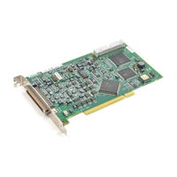
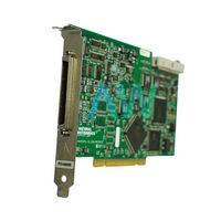
PCI E Series Multifunction I/O Boards for PCI Bus Computers
Brand:
National Instruments
| Category:
Computer Hardware
| Size: 1 MB
Table of Contents
Important Information
3
Table of Contents
4
About this Manual
9
Organization of this Manual
9
Conventions Used in this Manual
10
National Instruments Documentation
11
Related Documentation
12
Customer Communication
13
Chapter 1 Introduction
15
About the PCI E Series
15
What You Need to Get Started
16
Software Programming Choices
16
National Instruments Application Software
17
NI-DAQ Driver Software
17
Figure 1-1. the Relationship between the Programming Environment
18
NI-DAQ, and Your Hardware
18
Register-Level Programming
19
Optional Equipment
19
Custom Cabling
20
Unpacking
21
Chapter 2 Installation and Configuration
22
Software Installation
22
Hardware Installation
22
Board Configuration
23
Chapter 3 Hardware Overview
24
Figure 3-1. PCI-MIO-16E-1, PCI-MIO-16E-4 and PCI-6071E Block Diagram
24
Figure 3-2. PCI-MIO-16XE-10 and PCI-6031E Block Diagram
25
Figure 3-3. PCI-6032E and PCI-6033E Block Diagram
26
Analog Input
27
Figure 3-4. PCI-MIO-16XE-50 Block Diagram
27
Input Mode
27
Input Polarity and Input Range
28
Table 3-1. Available Input Configurations for the PCI E Series
28
Considerations for Selecting Input Ranges
31
Table 3-3. Actual Range and Measurement Precision, PCI-MIO-16XE-10 PCI-MIO-16XE-50, PCI-6031E, PCI-6032E, and PCI-6033E
31
Dither
32
Figure 3-5. Dither
33
Multichannel Scanning Considerations
33
Analog Output
35
Analog Output Reference Selection
35
Analog Output Polarity Selection
35
Analog Output Reglitch Selection
36
Analog Trigger
37
Figure 3-6. Analog Trigger Block Diagram
37
Figure 3-7. Below-Low-Level Analog Triggering Mode
38
Figure 3-8. Above-High-Level Analog Triggering Mode
38
Figure 3-9. Inside-Region Analog Triggering Mode
39
Figure 3-10. High-Hysteresis Analog Triggering Mode
39
Digital I/O
40
Timing Signal Routing
40
Figure 3-11. Low-Hysteresis Analog Triggering Mode
40
Figure 3-12. CONVERT* Signal Routing
41
Board and RTSI Clocks
42
Programmable Function Inputs
42
RTSI Triggers
42
Figure 3-13. RTSI Bus Signal Connection
43
Chapter 4 Signal Connections
44
I/O Connector
44
Figure 4-1. I/O Connector Pin Assignment for the PCI-MIO-16E-1
45
Figure 4-2. I/O Connector Pin Assignment for the PCI-6071E, 6031E, and 6033E
46
I/O Connector Signal Descriptions
47
Analog Input Signal Connections
55
Figure 4-3. PCI E Series PGIA
56
Types of Signal Sources
57
Floating Signal Sources
57
Ground-Referenced Signal Sources
57
Input Configurations
57
Figure 4-4. Summary of Analog Input Connections
58
Differential Connection Considerations (DIFF Input Configuration)
59
Differential Connections for Ground-Referenced Signal Sources
60
Figure 4-5. Differential Input Connections for Ground-Referenced Signals
60
Differential Connections for Nonreferenced or Floating Signal Sources
61
Figure 4-6. Differential Input Connections for Nonreferenced Signals
61
Single-Ended Connection Considerations
63
Figure 4-7. Single-Ended Input Connections for Nonreferenced or Floating Signals
64
Single-Ended Connections for Floating Signal Sources (RSE Configuration)
64
Single-Ended Connections for Grounded Signal Sources (NRSE Configuration)
64
Common-Mode Signal Rejection Considerations
65
Figure 4-8. Single-Ended Input Connections for Ground-Referenced Signals
65
Analog Output Signal Connections
66
Digital I/O Signal Connections
67
Figure 4-9. Analog Output Connections
67
Figure 4-10. Digital I/O Connections
68
Power Connections
69
Timing Connections
69
Programmable Function Input Connections
70
Figure 4-11. Timing I/O Connections
70
DAQ Timing Connections
71
Figure 4-12. Typical Posttriggered Acquisition
71
EXTSTROBE* Signal
72
Figure 4-13. Typical Pretriggered Acquisition
72
Figure 4-14. SCANCLK Signal Timing
72
SCANCLK Signal
72
Figure 4-15. EXTSTROBE* Signal Timing
73
TRIG1 Signal
73
Figure 4-16. TRIG1 Input Signal Timing
74
Figure 4-17. TRIG1 Output Signal Timing
74
TRIG2 Signal
74
Figure 4-18. TRIG2 Input Signal Timing
75
Figure 4-19. TRIG2 Output Signal Timing
75
Figure 4-20. STARTSCAN Input Signal Timing
76
STARTSCAN Signal
76
CONVERT* Signal
77
Figure 4-21. STARTSCAN Output Signal Timing
77
Figure 4-22. CONVERT* Input Signal Timing
78
Figure 4-23. CONVERT* Output Signal Timing
78
AIGATE Signal
79
SISOURCE Signal
79
Figure 4-24. SISOURCE Signal Timing
80
Waveform Generation Timing Connections
80
WFTRIG Signal
80
Figure 4-25. WFTRIG Input Signal Timing
81
Figure 4-26. WFTRIG Output Signal Timing
81
UPDATE* Signal
81
Figure 4-27. UPDATE* Input Signal Timing
82
Figure 4-28. UPDATE* Output Signal Timing
82
UISOURCE Signal
82
Figure 4-29. UISOURCE Signal Timing
83
General-Purpose Timing Signal Connections
83
GPCTR0_SOURCE Signal
83
Figure 4-30. GPCTR0_SOURCE Signal Timing
84
GPCTR0_GATE Signal
84
Figure 4-31. GPCTR0_GATE Signal Timing in Edge-Detection Mode
85
Figure 4-32. GPCTR0_OUT Signal Timing
85
GPCTR0_OUT Signal
85
GPCTR0_UP_DOWN Signal
85
Figure 4-33. GPCTR1_SOURCE Signal Timing
86
GPCTR1_GATE Signal
86
GPCTR1_SOURCE Signal
86
Figure 4-34. GPCTR1_GATE Signal Timing in Edge-Detection Mode
87
Figure 4-35. GPCTR1_OUT Signal Timing
87
GPCTR1_OUT Signal
87
Figure 4-36. GPCTR Timing Summary
88
GPCTR1_UP_DOWN Signal
88
FREQ_OUT Signal
89
Field Wiring Considerations
89
Chapter 5 Calibration
91
Loading Calibration Constants
91
Self-Calibration
92
External Calibration
92
Other Considerations
93
Appendix A Specifications
94
Bus Interface
104
Input Characteristics
106
Bandwidth (-3 Db)
108
Input Impedance
108
Dynamic Characteristics
108
Settling Time for Full-Scale Step
108
Gain Temperature Coefficient
109
Offset Temperature Coefficient
109
Noise
110
Compatibility
111
Number of Channels
111
Glitch Energy (at Midscale Transition) Magnitude
119
Figure B-1. 68-Pin E Series Connector Pin Assignments
123
Figure B-2. 68-Pin Extended Analog Input Connector Pin Assignments
124
Figure B-3. 50-Pin E Series Connector Pin Assignments
125
Figure B-4. 50-Pin Extended Analog Input Connector Pin Assignments
126
General Information
127
Technical Support Form
134
Advertisement
National Instruments PCI-MIO-16E-4 Programmer's Manual (162 pages)
Register-Level Programmer Manual, Multifunction I/O Boards for PCI Bus Computers, Register-Level
Brand:
National Instruments
| Category:
I/O Systems
| Size: 1.04 MB
Table of Contents
Table of Contents
4
About this Manual
9
Conventions Used in this Manual
10
Organization of this Manual
10
Customer Communication
11
Related Documentation
11
Chapter 1 General Description
12
General Characteristics
12
Chapter 2 Theory of Operation
14
Figure 2-1. PCI-MIO-16E-1, PCI-MIO-16E-4, and PCI-6071E Block Diagram
14
Functional Overview
14
Figure 2-2. PCI-MIO-16XE-10, PCI-6052E, and PCI-6031E Block Diagram
15
Figure 2-3. PCI-6023E, PCI-6024E, and PCI-6025E Block Diagram
16
Figure 2-4. PCI-6032E and PCI-6033E Block Diagram
17
Figure 2-5. PCI-MIO-16XE-50 Block Diagram
18
PCI Interface Circuitry
19
Analog Input and Timing Circuitry
20
Figure 2-6. PCI Bus Interface Circuitry Block Diagram
20
Analog Input Circuitry
21
Figure 2-7. Analog Input and Data Acquisition Circuitry Block Diagram
21
Table 2-1. PGIA Gain Set Verses Board
22
Data Acquisition Timing Circuitry
24
Single-Read Timing
24
Data Acquisition Sequence Timing
25
Figure 2-8. ADC Timing
25
Figure 2-9. Timing of Scan in Example 1
27
Figure 2-10. Multirate Scanning of Two Channels
28
Figure 2-11. Multirate Scanning of Two Channels with 1:X Sampling Rate
28
Figure 2-12. Multirate Scanning of Two Channels with 3:1:1 Sampling Rate
29
Figure 2-13. Multirate Scanning of Three Channels with 4:2:1 Sampling Rate
29
Figure 2-14. Multirate Scanning Without Ghost
30
Figure 2-16. Successive Scans Using Ghost
30
Posttrigger and Pretrigger Acquisition
31
Table 2-2. Analog Input Configuration Memory
31
Analog Triggering
32
Analog Output and Timing Circuitry
33
Figure 2-17. Analog Output Circuitry Block Diagram
33
Analog Output Circuitry
34
Analog Output Timing Circuitry
35
Single-Point Output
35
Waveform Generation
36
Digital I/O Circuitry
37
Figure 2-18. DAQ-STC Counter Diagram
37
Timing I/O Circuitry
37
RTSI Bus Interface Circuitry
38
Figure 2-19. RTSI Bus Interface Circuitry Block Diagram
39
Chapter 3 Register Map and Descriptions
40
Register Map
40
Table 3-1. PCI E Series Register Map
41
Register Sizes
42
Register Descriptions
42
Misc Register Group
42
Table 3-2. PCI E Series Windowed Register Map
42
Serial Command Register
43
Misc Command Register
44
Status Register
45
Analog Input Register Group
46
ADC FIFO Data Register
47
Configuration Memory Low Register
48
Table 3-3. PGIA Gain Selection
49
Configuration Memory High Register
50
Table 3-4. Calibration Channel Assignments
51
Table 3-5. Differential Channel Assignments
52
Table 3-6. Nonreferenced Single-Ended Channel Assignments
52
Table 3-7. Referenced Single-Ended Channel Assignments
53
Analog Output Register Group
54
Table 3-8. Auxiliary Channel Assignments
54
Table 3-9. Channel Assignments
54
AO Configuration Register
55
DAC FIFO Data Register
57
DAC0 Direct Data Register
58
DAC1 Direct Data Register
59
DMA Control Register Group
60
AI AO Select Register
61
G0 G1 Select Register
62
DAQ-STC Register Group
63
FIFO Strobe Register Group
63
ADC FIFO Clear Register
63
Configuration Memory Clear Register
63
DAC FIFO Clear Register
63
Chapter 4 Programming
64
Pcl Local Bus
64
PCI Initialization for the IBM Compatible System
65
Re-Mapping the PCI E Series Board
66
PCI Initialization for the Macintosh
67
Programming Examples
68
Windowing Registers
68
Digital I/O
70
Example 1
70
Example 2
70
Analog Input
71
Example 1
72
Example 2
75
Example 3
77
Example Program
78
Example 4
80
Programming the MITE for Different DMA Transfers
83
Call the Function Number_Of_Scans to Load the Number of Scans
84
AI Configuration Start = 1; Ai_Sc_Load_A_Registers (24 Bits) Number of Posttrigger Scans -1 = 4; Ai_Command_1_Register
84
AI SC Load = 1
84
Joint_Reset_Register
84
Example 5
84
Perform Analog Input Example 1 Step 1
84
Perform Analog Input Example 1 Step 2 for each Channel in the Scan List. Only Channel 0 Has Last Channel Set to
84
Perform Analog Input Example 1 Steps
84
Example 6
86
Example 7
88
Joint_Reset_Register
88
Example 8
90
AI Configuration Start = 0; AI Configuration End = 1; the Function Ai_Scan_Start
90
Perform Analog Input Example 1 Step
90
Example 9
92
The Function Ai_Scan_Start Selects the Scan Start Event
90
AI Configuration Start = 0; AI Configuration End
90
AI Configuration Start = 1
90
Ai_Command_1_Register
90
Joint_Reset_Register
90
Analog Output
94
Example 1
95
Example 2
97
Example 2
102
Example 3
102
Example 3
104
Example 4
104
Example 5
106
Example Program
106
General-Purpose Counter/Timer
108
Example 1
108
Example 2
110
Example 3
112
Analog Triggering
115
RTSI Trigger Lines Programming Considerations
115
Figure 4-1. Analog Trigger Structure
117
Interrupt Programming
119
Interrupt Sharing
119
DMA Programming
120
Figure 4-2. DMA Structure
120
The Link Chaining Mode for DMA Transfer
121
Figure 4-3. DMA Link Chaining Mode Structure
122
Chapter 5 Calibration
123
About the EEPROM
123
Figure 5-1. EEPROM Read Timing
124
Table 5-1. PCI-MIO-16E-1, PCI-MIO-16E-4, PCI-6071E EEPROM Map
125
Table 5-2. PCI-MIO-16XE-50 EEPROM Map
127
Table 5-3. PCI-MIO-16XE-10, PCI-6031E, PCI-6032E and PCI-6033E EEPROM Map
129
Table 5-4. PCI-6023E EEPROM Map
131
Table 5-5. PCI-6024E and PCI-6025E EEPROM Map
132
Table 5-6. PCI-6052E EEPROM Map
134
Calibration Dacs
136
Figure 5-2. Calibration AC Write Timing
138
NI-DAQ Calibration Function
139
Appendix A Customer Communication
140
Glossary
145
Index
152
National Instruments PCI-MIO-16E-4 Note To Users (3 pages)
Pinout Label for the SCB-68A
Brand:
National Instruments
| Category:
Control Unit
| Size: 1.47 MB
Advertisement
Advertisement
Related Products
National Instruments PCI-MIO-16E-1
National Instruments PCI-MIO-16XE-10
National Instruments PCI-MIO-16XE-50
National Instruments DAQ PCI-6025E
National Instruments PCI-6110E/6111E
National Instruments PCI-6032E
National Instruments PCI-8430
National Instruments PCI-8432
National Instruments PCI-CAN/2
National Instruments NI PCIe-7851R
National Instruments Categories
Control Unit
I/O Systems
Controller
Computer Hardware
Measuring Instruments
More National Instruments Manuals
Login
Sign In
OR
Sign in with Facebook
Sign in with Google
Upload manual
Upload from disk
Upload from URL