Sign In
Upload
Manuals
Brands
Motorola Manuals
Computer Hardware
MVME3600 Series
Motorola MVME3600 Series Manuals
Manuals and User Guides for Motorola MVME3600 Series. We have
1
Motorola MVME3600 Series manual available for free PDF download: Programmer's Reference Manual
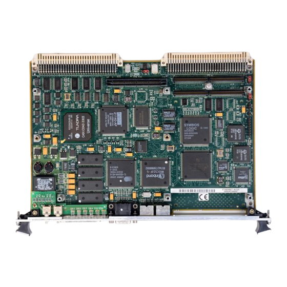
Motorola MVME3600 Series Programmer's Reference Manual (275 pages)
VME Processor Modules
Brand:
Motorola
| Category:
Computer Hardware
| Size: 1.33 MB
Table of Contents
Table of Contents
7
Overview of Contents
20
Summary of Changes
20
Comments and Suggestions
21
Conventions Used in this Manual
21
CHAPTER 1 Board Description and Memory Maps
25
Introduction
25
Overview
25
Summary of Features
26
Table 1-1. MVME3600/4600 Series Features Summary
26
Block Diagrams
27
Figure 1-1. MVME3600 Series System Block Diagram
29
Figure 1-2. MVME4600 Series System Block Diagram
30
Functional Description
31
Overview
31
Programming Model
32
Memory Maps
32
Processor Memory Maps
32
Table 1-2. Default Processor Memory Map
33
Table 1-3. CHRP Memory Map Example
34
Table 1-4. Raven MPC Register Values for CHRP Memory Map
35
Table 1-5. PREP Memory Map Example
36
Table 1-6. Raven MPC Register Values for PREP Memory Map
37
PCI Memory Maps
38
Table 1-7. PCI CHRP Memory Map
38
Table 1-8. Raven PCI Register Values for CHRP Memory Map
40
Table 1-9. Universe PCI Register Values for CHRP Memory Map
40
Table 1-10. PCI PREP Memory Map
41
Table 1-11. Raven PCI Register Values for PREP Memory Map
43
Table 1-12. Universe PCI Register Values for PREP Memory Map
43
Vmebus Mapping
44
Figure 1-3. Vmebus Master Mapping
45
Figure 1-4. Vmebus Slave Mapping
47
Table 1-13. Universe PCI Register Values for Vmebus Slave Map Example
48
Falcon-Controlled System Registers
49
Table 1-14. Vmebus Slave Map Example
49
Table 1-15. System Register Summary
49
System Configuration Register (SYSCR)
50
Memory Configuration Register (MEMCR)
51
System External Cache Control Register (SXCCR)
53
CPU Control Register
55
ISA Local Resource Bus
55
W83C553 PIB Registers
55
PC87308VUL Super I/O (ISASIO) Strapping
56
NVRAM/RTC & Watchdog Timer Registers
56
Table 1-16. Strap Pins Configuration for the PC87308VUL
56
Module Configuration and Status Registers
57
Table 1-17. MK48T59/559 Access Registers
57
Table 1-18. Module Configuration and Status Registers
57
Base Module Feature Register
58
CPU Configuration Register
58
Base Module Status Register (BMSR)
59
Seven-Segment Display Register
60
VME Registers
61
LM/SIG Control Register
61
LM/SIG Status Register
61
Table 1-19. VME Registers
61
Location Monitor Upper Base Address Register
64
Location Monitor Lower Base Address Register
64
Semaphore Register 1
65
Semaphore Register 2
65
VME Geographical Address Register (VGAR)
66
Z85230 ESCC and Z8536 CIO Registers and Port Pins
67
Z8536/Z85230 Registers
67
Table 1-20. Z8536/Z85230 Access Registers
67
Z8536 CIO Port Pins
68
Table 1-21. Z8536 CIO Port Pins Assignment
68
Table 1-22. Interpretation of MID3-MID0
69
ISA DMA Channels
70
Table 1-23. PIB DMA Channel Assignments
71
CHAPTER 2 Raven PCI Host Bridge & Multi-Processor
73
Interrupt Controller Chip
73
Introduction
73
Summary of Features
73
Block Diagram
74
Functional Description
76
MPC Bus Interface
76
MPC Address Mapping
76
Figure 2-2. MPC to PCI Address Decoding
77
MPC Slave
78
Figure 2-3. MPC to PCI Address Translation
78
Table 2-1. MPC Slave Response Command Types
79
MPC Write Posting
80
MPC Master
80
Table 2-2. MPC Transfer Types
81
MPC Arbiter
82
MPC Bus Timer
82
PCI Interface
82
PCI Address Mapping
83
Figure 2-4. PCI to MPC Address Decoding
84
Figure 2-5. PCI to MPC Address Translation
85
PCI Slave
86
Table 2-3. PCI Slave Response Command Types
87
PCI Write Posting
89
PCI Master
89
Table 2-4. PCI Master Command Codes
90
Generating PCI Cycles
92
Figure 2-6. PCI Spread I/O Address Translation
94
Endian Conversion
97
When MPC Devices Are Big-Endian
97
When MPC Devices Are Little-Endian
98
Figure 2-7. Big to Little-Endian Data Swap
98
Raven Registers
99
Table 2-5. Address Modification for Little-Endian Transfers
99
Error Handling
100
Transaction Ordering
101
Registers
102
MPC Registers
102
Table 2-6. Raven MPC Register Map
102
Vendor ID/Device ID Registers
104
General Control-Status/Feature Registers
105
Revision ID Register
105
MPC Arbiter Control Register
107
Prescaler Adjust Register
108
MPC Error Status Register
111
MPC Error Address Register
113
PCI Interrupt Acknowledge Register
115
MPC Slave Address (3) Register
116
MPC Slave Offset/Attribute (0,1 and 2) Registers
117
MPC Slave Offset/Attribute (3) Registers
118
General Purpose Registers
119
Table 2-7. Raven PCI Configuration Register Map
120
Table 2-8. Raven PCI I/O Register Map
121
Vendor ID/ Device ID Registers
121
PCI Command/ Status Registers
122
Revision ID/ Class Code Registers
124
Memory Base Register
125
PCI Slave Address (0,1,2 and 3) Registers
126
PCI Slave Attribute/ Offset (0,1,2 and 3) Registers
127
CONFIG_ADDRESS Register
128
CONFIG_DATA Register
130
Raven Interrupt Controller Implementation
131
Csr's Readability
132
Spurious Vector Generation
133
Raven-Detected Errors
134
Figure 2-8. Ravenmpic Block Diagram
136
Block Diagram Description
136
Program Visible Registers
137
Interrupt Request Register (IRR)
138
MPIC Registers
140
Table 2-9. Ravenmpic Register Map
141
Feature Reporting Register
144
Global Configuration Register
145
Vendor Identification Register
146
IPI Vector/Priority Registers
147
Spurious Vector Register
148
Timer Current Count Registers
149
Timer Vector/Priority Registers
150
Timer Destination Registers
151
External Source Destination Registers
153
Raven-Detected Errors Destination Register
154
Interprocessor Interrupt Dispatch Registers
155
Interrupt Acknowledge Registers
156
End-Of-Interrupt Registers
157
Reset State
158
Operation
159
EOI Register
160
Architectural Notes
161
Introduction
163
Block Diagrams
164
Figure 3-1. Falcon Pair Used with DRAM in a System
165
Figure 3-2. Falcon Internal Data Paths (Simplified)
166
Figure 3-3. Overall DRAM Connections
167
Functional Description
168
CHAPTER 3 Falcon ECC Memory Controller Chipset
169
Single-Beat Reads/Writes
169
Table 3-1. Powerpc 60X Bus to DRAM Access Timing When Configured for 70Ns
170
Table 3-2. Powerpc 60X Bus to DRAM Access Timing When Configured for 60Ns
171
Table 3-3. Powerpc 60X Bus to DRAM Access Timing When Configured for 50Ns Hyper Devices
172
Rom/Flash Speeds
173
Table 3-4. Powerpc 60X Bus to Rom/Flash Access Timing When Configured for 64 Bits (32 Bits Per Falcon)
173
Table 3-5. Powerpc 60X Bus to Rom/Flash Access Timing When Configured for 16 Bits (8 Bits Per Falcon)
173
Powerpc 60X Bus Interface
174
Cache Coherency Restrictions
175
Table 3-6. Error Reporting
176
Error Logging
177
Table 3-7. Powerpc 60X to Rom/Flash Address Mapping When Rom/Flash
179
Table 3-8. Powerpc 60X to Rom/Flash Address Mapping When Rom/Flash
180
Refresh/Scrub
181
Blocks a And/Or B Present, Blocks C And/Or D Present
182
DRAM Arbitration
183
CSR Accesses
184
Figure 3-4. Data Path for Reads from the Falcon Internal Csrs
185
Figure 3-5. Data Path for Writes to the Falcon Internal Csrs
186
Figure 3-6. Memory Map for Byte Reads to the CSR
187
Figure 3-7. Memory Map for Byte Writes to the Internal Register Set
188
Figure 3-8. Memory Map for 4-Byte Reads to the CSR
189
Figure 3-9. Memory Map for 4-Byte Writes to the Internal Register Set
189
Register Summary
190
Table 3-9. Register Summary
191
Detailed Register Bit Descriptions
193
Vendor/Device Register
194
Table 3-10. Ram Spd1,Ram Spd0 and DRAM Type
195
DRAM Attributes Register
196
Table 3-11. Block_A/B/C/D Configurations
197
DRAM Base Register
198
CLK Frequency Register
199
ECC Control Register
200
Error Logger Register
204
Error_Address Register
206
Table 3-12. Rtest Encodings
207
Scrub/Refresh Register
207
Refresh/Scrub Address Register
208
ROM a Base/Size Register
209
Table 3-13. Rom/Flash Block a Size Encoding
210
Table 3-15. Read/Write to Rom/Flash
211
ROM B Base/Size Register
212
Table 3-16. Rom/Flash Block B Size Encoding
213
DRAM Tester Control Registers and Test SRAM
214
Power-Up Reset Status Register 1
215
External Register Set
216
Software Considerations
217
Sizing DRAM
218
Table 3-17. Sizing Addresses
220
Table 3-18. Powerpc 60X Address to DRAM Address Mappings
221
ECC Codes
221
Table 3-19. Syndrome Codes Ordered by Bit in Error
222
Table 3-20. Single-Bit Errors Ordered by Syndrome Code
223
Data Paths
224
Figure 3-10. Powerpc Data to DRAM Data Correspondence
225
Table 3-21. Powerpc Data to DRAM Data Mapping
226
CHAPTER 4 Universe (Vmebus to PCI) Chip
227
General Information
227
Functional Description
228
Figure 4-1. Architectural Diagram for the Universe
229
Vmebus Interface
230
PCI Bus Interface
231
Interrupter and Interrupt Handler
232
DMA Controller
233
Figure 4-2. UCSR Access Mechanisms
234
Universe Register Map
234
Table 4-1. Universe Register Map
235
Universe Chip Problems after a PCI Reset
239
Examples
241
Example 2: MVME3600 Series Board Acts Differently
243
Example 3: Universe Chip Is Checked at Tundra
245
Table 5-1. PCI Arbitration Assignments
247
Introduction
247
Figure 5-1. MVME3600/4600 Series Interrupt Architecture
248
CHAPTER 5 Programming Details
248
Interrupt Handling
248
Ravenmpic
249
Table 5-2. Ravenmpic Interrupt Assignments
249
Interrupts
250
Figure 5-2. PIB Interrupt Handler Block Diagram
251
Table 5-3. PIB PCI/ISA Interrupt Assignments
252
ISA DMA Channels
253
Table 5-4. Reset Sources and Devices Affected
254
Exceptions
254
Soft Reset
255
Table 5-5. Error Notification and Handling
256
Endian Issues
257
Figure 5-3. Big-Endian Mode
258
Figure 5-4. Little-Endian Mode
259
Processor/Memory Domain
260
PCI-Ethernet
261
Rom/Flash Initialization
262
APPENDIX A Related Documentation
263
Motorola Computer Group Documents
263
Manufacturers' Documents
264
Related Specifications
266
Advertisement
Advertisement
Related Products
Motorola MVME712-12
Motorola MVME712A/D3
Motorola MVME712AM
Motorola MVME712B
Motorola MVME5100 Series
Motorola MVME135A
Motorola MVME135-1
Motorola MVME136
Motorola MVME712C
Motorola MVME3100
Motorola Categories
Cell Phone
Two-Way Radio
Baby Monitor
Cordless Telephone
Radio
More Motorola Manuals
Login
Sign In
OR
Sign in with Facebook
Sign in with Google
Upload manual
Upload from disk
Upload from URL