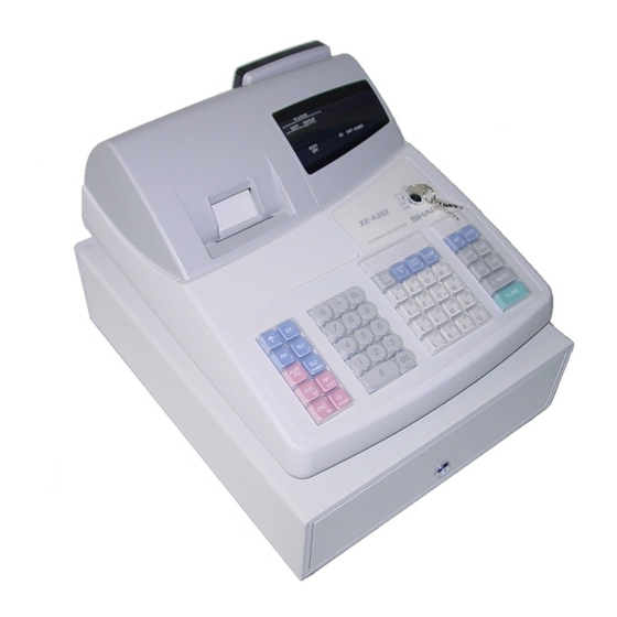
Sharp XE-A202 Service Manual
Electronic cash register
Hide thumbs
Also See for XE-A202:
- Instruction manual (354 pages) ,
- Quick start manual (6 pages) ,
- Quick setup (4 pages)
Table of Contents
Advertisement
q
Chapter 1. Specifications . . . . . . . . . . . . . . . . . . . . . . . . . . . . 1
Chapter 2. Options . . . . . . . . . . . . . . . . . . . . . . . . . . . . . . . . . . . 5
Chapter 3. Master Reset And Program Reset. . . . . . . . . 5
Chapter 4. Hardware Description . . . . . . . . . . . . . . . . . . . . 6
Chapter 5. Test Function . . . . . . . . . . . . . . . . . . . . . . . . . . . . 12
Chapter 8. Circuit Diagram And Pwb Layout . . . . . . . . . 17
Parts marked with "!" are important for maintaining the safety of the set. Be sure to replace these parts with specified
ones for maintaining the safety and performance of the set.
SERVICE MANUAL
CONTENTS
CONNECTING THE RS-232 CABLE . . . . . . . . . . . . . 16
SHARP CORPORATION
CODE : 00Z
ELECTRONIC
CASH REGISTER
XE-A202
MODEL
(V version)
This document has been published to be used
for after sales service only.
The contents are subject to change without notice.
XEA202VSME
Advertisement
Table of Contents

Related Manuals for Sharp XE-A202


Summary of Contents for Sharp XE-A202
- Page 1 CODE : 00Z XEA202VSME ELECTRONIC CASH REGISTER XE-A202 MODEL (V version) CONTENTS CHAPTER 1. SPECIFICATIONS ......1 CHAPTER 2.
-
Page 2: Mode Switch
CLK# Clerk code entry key 1-17~16-32 Department keys Value added tax key 2. RATING AUTO Automatic sequence key XE-A202 CR1, CR2 Credit 1 and 2 keys Weight 11.3kg CH1, CH2 Cheque 1 and 2 keys Dimensions 421 (W) x 429 (D) x 305 (H) mm... - Page 3 The mode switch has these settings: Customer display (Pop-up type) Operator display This mode locks all register operations. (AC power turns off.) No change occurs to register data. PLU/SUB Clerk code DEPT REPEAT OP X/Z: To take individual clerk X or Z reports, and to take flash reports.
- Page 4 6. PRINTER Segment Display Description 1) Printer position Amount • Part number : M-T53II Minus sign 2-10 -: Floating • NO. of station : 1 (Receipt or journal) Error 8-10 Exx:xx = error code • Validation : No. PGM Mode •...
- Page 5 7. DRAWER 8. BATTERY 1) MEMORY BACK UP BATTERY [OUTLINE] For memory back up, the dry battery AA (3 pieces) are needed. • Standard equipment: Yes (1) 1. Memory holding time: • Max. number of additional drawers: 0 Approx. 1 year after New dry batteries are installed. •...
-
Page 6: Master Resetting
CHAPTER 2. OPTIONS 1. OPTIONS (No) 2. SERVICE OPTIONS (No) 3. SUPPLIES PRICE NAME PARTS CODE DESCRIPTION RANK TPAPR2377RC05 Roll paper 5roll/pack 4. SPECIAL SERVICE TOOLS PRICE NAME PARTS CODE DESCRIPTION RANK UKOG-6705RCZZ RS-232 Loop-back connector POS tools3 (IPL Software) Software –... - Page 7 CHAPTER 4. HARDWARE DESCRIPTION 1. HARDWARE BLOCK DIAGRAM POWER SUPPLY STANDARD DRAWER. Data bus Address ROM : 256K Byte 128K Byte RAM : 20K Byte DRIVER , SENSOR POPUP Seg. DRIVER PRINTER FRONT M-T53 4 to 16 Dig. DRIVER DECORDER PAPER TAKE UP MOTOR KEYBOARD...
- Page 8 2) Pin description V0 24V TRANSFORMER PQ1CG2032 Drawer SIGNAL SYMBOL Function NAME SOUT4 Key IN CLK4 Key IN TB4IN Key IN /POFF detect point TB3IN Key IN PQ1CG2032 VLED 5.7V SOUT3 Key IN VCC 5V SIN3 Key IN VDD 5V CLK3 Key IN Battery...
-
Page 9: Reset Circuit
3. CLOCK GENERATOR SIGNAL SYMBOL Function NAME 1) CPU Address bus :17 Address bus :16 Address bus :15 Address bus :14 12MHz Address bus :13 Address bus :12 FS781 3.3K Address bus :11 XOUT 12MHz Address bus :10 220pF Address bus :9 XCOUT Address bus :8 32.768KHz... - Page 10 7. PRINTER CONTROL CIRCUIT The P-OFF signal detects two signals by two comparators and sent to the CPU. V0 (24V) signal: If the power voltage V0 (24V) falls bellow the specified 1) Paper feed motor circuit level, the P-OFF signal is driver to LOW by the com- parator ICAA.
- Page 11 9. DRAWER DRIVE CIRCUIT Thermal head block daigram Dot #288 Dot #1 5,6,18,19 T400mA/250V 9,10,14,15 0.1u IN4002 STB1 R102 /RTS0 (38pin) 2SD2212 STB2 FB2, FB3: Jumper Wire Latch register Shift register When the DR1 signal from the CPU is HIGH, Q9 is turned on to operate the solenoid.
- Page 12 1) Keyboard 5) Paper end sensor Scan signal: 10 /S0-9 signals Scan signal: 1 /S4 signal Return signal: 6 P92-97 signals Return signal: 1 P91 signal The keys are read by the key matrix following the above signals. The paper end sensor state is read by the above signals. Receipt near end sensor End detected End not detected...
- Page 13 CHAPTER 5. TEST FUNCTION 1. TEST ITEMS 2) KEY CODE 1 Key operation The test items are as follows: RCPT/PO Code Description 2 Test procedure Display buzzer test Key code Display Printer test KEY CODE Keyboard test 3 Check that: mode switch test KEY code: Every time a key is pressed, the code of that key is dis- Printer sensor test...
- Page 14 9 will be displayed.) B) The sensor correctly indicates the status of the drawer 1. 3 Check: *On the XE-A202, “C” (CLOSED) is always displayed. The display during testing and the content of the completion print. 4 End of testing 4 End of testing You can exit the test mode by pressing any key.
- Page 15 4 End of testing 12) AD conversion port The program ends after printing. 1 Key operation When the test ends normally. RCPT/PO When the test ends abnormally. Ex- ~ - ***** 2 Test procedure x = 1: Data error The test program displays the voltage of each AD port. x = 2: Address error 1 6 0 1 X X X...
- Page 16 CHAPTER 6. IPL (INITIAL PROGRAM LOADING) FUNCTION The application program of the XE-A202 is written into the Flash ROM <IPL software on PC> in the CPU. 7) Copy the following files in "PosUtilityTool3" into the hard disk of PC. Since the CPU supplied as a service part does not include the applica- Postool3.exe...
- Page 17 APPENDIX: RS232C CABLE CHAPTER 7. CAUTION TO BE USED WHEN CONNECTING The RS-232C cable has the following internal connections: THE RS-232 CABLE (Equivalent to a cross cable used in the conventional connection of ECR-ECR) When connecting the RS-232 cable to the XE-A212, be sure to observe the following condiiton: 9PIN D-SUB 9PIN D-SUB...
- Page 18 BUSY /FRDY XE-A202V CIRCUIT DIAGRAM AND PWB LAYOUT – 17 –...
- Page 19 XE-A202V CIRCUIT DIAGRAM AND PWB LAYOUT – 18 –...
- Page 20 XE-A202V CIRCUIT DIAGRAM AND PWB LAYOUT – 19 –...
- Page 21 XE-A202V CIRCUIT DIAGRAM AND PWB LAYOUT – 20 –...
- Page 22 XE-A202V CIRCUIT DIAGRAM AND PWB LAYOUT – 21 –...
- Page 23 XE-A202V CIRCUIT DIAGRAM AND PWB LAYOUT – 22 –...
- Page 24 XE-A202V CIRCUIT DIAGRAM AND PWB LAYOUT – 23 –...
- Page 25 2. KEY INTERFACE PWB LAYOUT A. side B. side 3. PRINTER I/F PWB LAYOUT XE-A202V CIRCUIT DIAGRAM AND PWB LAYOUT – 24 –...
- Page 26 4. REAR DISPLAY PWB LAYOUT 5. DISPLAY PWB LAYOUT XE-A202V CIRCUIT DIAGRAM AND PWB LAYOUT – 25 –...
- Page 27 © COPYRIGHT 2003 BY SHARP CORPORATION All rights reserved. Printed in Japan. No part of this publication may be reproduced, stored in a retrieval system, or transmitted. In any form or by any means, electronic, mechanical, photocopying, recording, or otherwise, without prior written permission of the publisher.