Table of Contents
Advertisement
Quick Links
GUITAR AMPLIFIER
SERVICE MANUAL
CONTENTS
SPECIFICATIONS ····································································· 3
PANEL LAYOUT········································································ 4
CIRCUIT BOARD LAYOUT ······················································· 5
BLOCK DIAGRAM ····································································· 6
DISASSEMBLY PROCEDURE·················································· 6
LSI PIN DESCRIPTION ····························································· 8
IC BLOCK DIAGRAM ······························································ 10
SELF CHECK AND INSPECTIONS ········································ 12
PARTS LIST
OVERALL CIRCUIT DIAGRAM
CIRCUIT BOARDS
GA
011476
HAMAMATSU, JAPAN
19990901-65000
1.615K-455
Printed in Japan '99.08
Advertisement
Chapters
Table of Contents

Related Manuals for Yamaha DG60-112


Summary of Contents for Yamaha DG60-112
-
Page 1: Circuit Boards
GUITAR AMPLIFIER SERVICE MANUAL CONTENTS SPECIFICATIONS ····································································· 3 PANEL LAYOUT········································································ 4 CIRCUIT BOARD LAYOUT ······················································· 5 BLOCK DIAGRAM ····································································· 6 DISASSEMBLY PROCEDURE·················································· 6 LSI PIN DESCRIPTION ····························································· 8 IC BLOCK DIAGRAM ······························································ 10 SELF CHECK AND INSPECTIONS ········································ 12 PARTS LIST OVERALL CIRCUIT DIAGRAM CIRCUIT BOARDS 011476... -
Page 2: Specifications
IMPORTANT NOTICE This manual has been provided for the use of authorized Yamaha Retailers and their service personnel. It has been assumed that basic service procedures inherent to the industry, and more specifically Yamaha Products, are already known and understood by the users, and have therefore not been restated. -
Page 3: Specifications
DG60-112 SPECIFICATIONS Digital Section D/A Converter 20 bit Complete Digital Signal Processing Amplification Type: Internal 8 Channel Preset Sampling Frequency 48 kHz Digital Reverb (SPRING) Speaker Simulator (LINE OUT) Input Level/Impedance INPUT HIGH: –20 dBm (THRU)/1 MΩ Analog Section INPUT LOW: –10 dBm (THRU)/1 MΩ... -
Page 4: Panel Layout
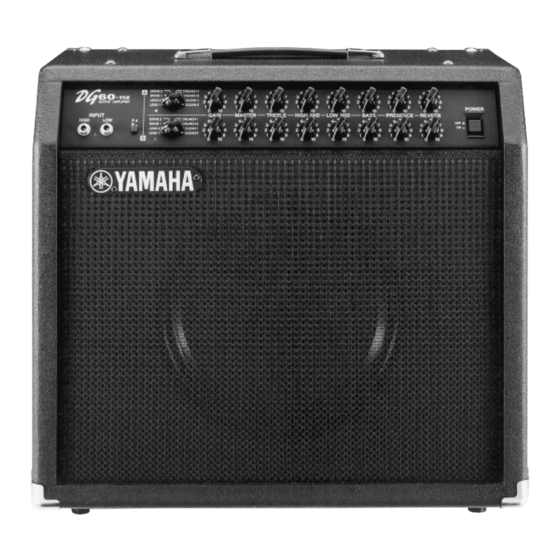
DG60-112 PANEL LAYOUT Front Panel Input Jack (INPUT HIGH, LOW) Peak Indicator Channel Select Switch Channel Indicator Amp Select Switch Gain Volume (GAIN) Master Volume (MASTER) Tone Controls (TREBLE, HIGH MID, LOW MID, BASS, PRESENCE) Reverb Volume (REVERB) Power Switch (POWER) -
Page 5: Circuit Board Layout
DG60-112 CIRCUIT BOARD LAYOUT (Bottom) • Rear view (Top) • Side view MAIN MAIN MAIN MAIN AC cord • Top view Power transformer MAIN MAIN A-CH A-CH • Front view MAIN... -
Page 6: Block Diagram
DG60-112 BLOCK DIAGRAM DISASSEMBLY PROCEDURE Pre-Main Unit Remove the four (4) screws marked [70]. The back board (U) can then be removed. (Fig. 1) Remove the speaker wires and the screw marked [120]. (Fig. 1) Remove the four (4) screws marked [30]. The pre-main unit can then be removed by sliding it backward. -
Page 7: Ground
DG60-112 MAIN (1/5-5/5), A-CH and SW Circuit Boards Remove the pre-main unit. (See Procedure 1.) Each circuit board can then be removed in its manner as below. (Fig. 2) MAIN 1/5 Circuit Board Remove the eight (8) knobs marked [90B], the eight (8) hexagonal nuts marked [A], the two (2) hexagonal nuts marked [130B] and the five (5) screws marked [80B]. -
Page 8: Chip Select
DG60-112 LSI PIN DESCRIPTION HD6433042SC10FP (XW325100) CPU DM: IC17 NAME FUNCTION NAME FUNCTION Port A Address bus Power supply Address bus Port B Ground P60//WAIT PB6//DREQ0 P61//BREQ Port 6 PB7//DREQ1 /RESO Reset P62//BACK Ground Ø Ø out P90/TXD0 Transmit data (MIDI OUT) -
Page 9: Chip Select
DG60-112 YSS228E-F (XQ962D00) DSP3 (Digital Signal Processor) DM: IC14, 15 NAME FUNCTION NAME FUNCTION Ground Ground System master clock input (60 M or30 MHz) DB13 System master clock input (60 M or30 MHz) DB14 Power supply DB15 /SYNCI System synch. input... -
Page 10: Ic Block Diagram
DG60-112 AK4520A-VF-E2 (XT802A00) ADC & DAC MAIN: IC301 NAME FUNCTION NAME FUNCTION VREFH Positive Voltage Reference Input, VA MCLK Master Clock Input VREFL Negative Voltage Reference Input, AGND DEM0 De-emphasis Frequency Select AINR+ Rch Analog Positive Input DEM1 De-emphasis Frequency Select... -
Page 11: Ground
DG60-112 TC74HC4040F (XR684A00) TC74HC4052AF (XS790A00) NE5532P (IG102500) 12-Stage Binary Ripple Counter Differential 4-Channnel NJM4556AD (XQ824A00) Multiplexer/Demultiplexer Dual Operational Amplifier DM: IC 8 DM: IC 19, 20 DM: IC 1, 2, 4–6 +DC Voltage Output A Y-COM Y-COM Supply Inverting Output B... -
Page 12: Self Check And Inspections
LED Check When the DG60-112 enters the self check mode, the LED check is started and the LEDs light automatically as the check follows the circular sequence below, while pressing the SW2 switch. all LEDs on... - Page 13 DG60-112 When fully turning the check volume knob counterclockwise, the A ch LED (CN5–2 pin) will light; when fully turning it clockwise, the B ch LED (CN5–3) will light. If the volume is no good, both the A ch and B ch LEDs (CN5–2, 3 pin) will light to indicate the error.
-
Page 14: Port
GUITAR AMPLIFIER PARTS LIST CONTENTS OVERALL ASSEMBLY ·········································································································································· 2 PRE-MAIN UNIT ···················································································································································· 4 OVERALL CABINET ASSEMBLY·························································································································· 6 ELECTRICAL PARTS ······································································································································ 7~12 Notes : DESTINATION ABBREVIATIONS Australian model M: South African model British model Chinese model Canadian model South-east Asia model German model Taiwan model European model... -
Page 15: Overall Assembly
DG60-112 OVERALL ASSEMBLY Pre-main unit: See page 4. Overall cabinet assembly: See page 6. - Page 16 DG60-112 PART NO. DESCRIPTION REMARKS REF NO. RANK OVERALL ASSEMBLY DG60-112 Overall Assembly (V369020) Overall Assembly (V369030) Overall Assembly (V369040) Overall Assembly (V369050) Pre-main Unit (V369130) Pre-main Unit (V369140) Pre-main Unit (V369150) Pre-main Unit (V369160) V3691700 Overall Cabinet Assembly VP104600 Oval Head Screw 5.0X35 MFC2BL...
-
Page 17: Pre-Main Unit
DG60-112 PRE-MAIN UNIT 200 190 130 140 U model: not used... - Page 18 DG60-112 PART NO. DESCRIPTION REMARKS REF NO. RANK PRE-MAIN UNIT DG60-112 Pre-main Unit (V369130) Pre-main Unit (V369140) Pre-main Unit (V369150) Pre-main Unit (V369160) V3692500 Chassis V3817700 Chassis V3817800 Chassis V3755700 Insulation Sheet AAX07370 Circuit Board MAIN AAX07380 Circuit Board MAIN...
-
Page 19: Overall Cabinet Assembly
DG60-112 OVERALL CABINET ASSEMBLY Handle assembly 10 15 PART NO. DESCRIPTION REMARKS REF NO. RANK V3691700 OVERALL CABINET ASSEMBLY DG60-112 Cabinet Assembly (V369420) Vinyl (V369430) Speaker Net (V369860) V3694400 Corner Protector V3833600 Round Head Tapping Screw-1 3.5X16 MFNI33 V3630300 Handle Assembly... -
Page 20: Electrical Parts
DG60-112 ELECTRICAL PARTS PART NO. DESCRIPTION REMARKS REF NO. RANK ELECTRICAL PARTS DG60-112 V3732600 Circuit Board (XV996A0) AAX07370 Circuit Board MAIN (XV964B0) AAX07380 Circuit Board MAIN (XV964B0) AAX07370 Circuit Board A-CH (XV964B0) AAX07380 Circuit Board (XV964B0) V3732600 Circuit Board (XV996A0) UN857100 Electrolytic Cap.-BP... - Page 21 DG60-112 PART NO. DESCRIPTION REMARKS REF NO. RANK UB245100 Monolithic Ceramic Cap. F 0.100 25V Z UR828100 Electrolytic Cap. 100.00 10.0V UB245100 Monolithic Ceramic Cap. F 0.100 25V Z UB245100 Monolithic Ceramic Cap. F 0.100 25V Z UR847100 Electrolytic Cap.
- Page 22 DG60-112 PART NO. DESCRIPTION REMARKS REF NO. RANK HF755470 Carbon Resistor 470.0 1/4 J VA074400 Metal Film Resistor 10.0K 1/5 F VB064100 Metal Film Resistor 470.0 1/5 F VB066500 Metal Film Resistor 2.7K 1/5 F HF756560 Carbon Resistor 5.6K 1/4 J...
- Page 23 DG60-112 PART NO. DESCRIPTION REMARKS REF NO. RANK AAX07370 Circuit Board A-CH (XV964B0) AAX07380 Circuit Board (XV964B0) V3690100 LED Holder LED3-4A VV319600 Fuse Holder CQ-05CT VV291400 Jumper Wire 0.60 BT201 Cable Kit #18 1P L 100 (V363230) (V363240) BT202 Connector Assembly...
- Page 24 DG60-112 PART NO. DESCRIPTION REMARKS REF NO. RANK IC201 IG107000 NJM072D OP AMP IC202 IG107000 NJM072D OP AMP IC203 XJ607A00 NJM7805FA REGULATOR +5V JK201 V3633400 Phone Jack HTJ-064-12I INPUT HIGH JK202 V3633400 Phone Jack HTJ-064-12I INPUT LOW LD201 VV620800 LT311G-41-C13 RE...
- Page 25 DG60-112 PART NO. DESCRIPTION REMARKS REF NO. RANK TR204 IA097030 Transistor 2SA970 GR,BL TR205 IA097030 Transistor 2SA970 GR,BL TR206 VE198800 Transistor 2SC2705 O,Y TR207 IC342100 Transistor 2SC3421 O,Y TR208 IA135800 Transistor 2SA1358 O,Y TR209 VZ222300 Pair Transistor A1492C3856(Z)(210) TR210 IC342100...
-
Page 26: Parts List
DG60-112 OVERALL CIRCUIT DIAGRAM 1/2 ( DM ) DG60-112 LINE OUT/ PHONES OP AMP ADC / DAC to MAIN 1/5-W201 SEND OP AMP EFFECT BLEND 0dB / -20dB RETURN INVERTER SHIFT REGISTER D-FF to MAIN 1/5-W202 OP AMP REGULATOR COUNTER... -
Page 27: Overall Circuit Diagram
DG60-112 OVERALL CIRCUIT DIAGRAM 2/2 ( MAIN, A-CH, SW ) DG60-112 to DM-CN1 to DM-CN2 MAIN OP AMP Peak indicator OP AMP Power transformer AC cord Cord strain relief XV965A00 VZ461100 VV103000 MAIN U, C XV966A00 VV205600 VV103100 XV967A00 VV058200...