Kenwood DDX6019 Service Manual
Monitor with dvd receiver
Hide thumbs
Also See for DDX6019:
- Instruction manual (88 pages) ,
- Installation manual (25 pages) ,
- Instruction manual (102 pages)
Table of Contents
Advertisement
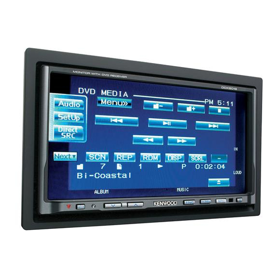
MONITOR WITH DVD RECEIVER
DDX6019/6029
/6029Y/6039
SERVICE MANUAL
DC cord (DDX6019/6039)
(E30-6530-05)
DC cord (DDX6029/6029Y)
(E30-6531-05)
* Refer to the parts list.
Panel assy
(A64-)*
MONITOR WITH DVD RECEIVER
ATT
Escutcheon
(B07-3172-12)
Remote Controller assy
(A70-2077-05)
RC-DV430
© 2006-3 PRINTED IN JAPAN
B53-0390-00 ( N ) 960
Escutcheon
(B07-3173-01)
Lever
Screw set
(D10-4674-04) x 2
(DDX6019/6039)
(N99-1776-05)
This product uses Lead Free solder.
Mounting hardware
(J22-0498-03)
1
Antenna adaptor
(DDX6029/6029Y)
(T90-0552-05)
Advertisement
Table of Contents

Related Manuals for Kenwood DDX6019


Summary of Contents for Kenwood DDX6019
-
Page 1: Service Manual
MONITOR WITH DVD RECEIVER DDX6019/6029 /6029Y/6039 SERVICE MANUAL © 2006-3 PRINTED IN JAPAN B53-0390-00 ( N ) 960 Panel assy (A64-)* MONITOR WITH DVD RECEIVER DC cord (DDX6019/6039) Escutcheon Escutcheon Mounting hardware (E30-6530-05) (B07-3172-12) (B07-3173-01) (J22-0498-03) DC cord (DDX6029/6029Y) Remote controller assy... -
Page 3: Block Diagram
DDX6019/6029/6029Y/6039 BLOCK DIAGRAM DVD unit (X37-1150) DVD UNIT (X37-1150-00) S3.3V DISC RESET IC A3.3V 16.897849MHz VPU1 IC65 DVD LD/CD LD SPINDLE S5V A3.3V S3.3V 1.5V A3.3V CN10 : Q7,8 MOTOR VC(2.2V) 40PIN IMON/VR OPTICAL PICKUP I/V OUT(DVD/CD) LOP-(AD) THERMISTER FO+/-,TR+/- A3.3V... - Page 4 DDX6019/6029/6029Y/6039 COMPONENTS DESCRIPTION RECEIVER UNIT (X14-974x-xx) Ref. No Application / Function Operation / Condition / Compatibility Logic IC (NOR x 4) Hard MUTE DRIVER 3 terminal regulator Audio8V, Tuner8V generating IC101 100 pin -com Primarily, audio board control IC104 Voltage detector -com reset voltage (4.2V) monitoring...
- Page 5 DDX6019/6029/6029Y/6039 COMPONENTS DESCRIPTION Ref. No Application / Function Operation / Condition / Compatibility Q304 Transistor Pre-Out Mute (RL) Q305 Transistor Pre-Out Mute (RR) Q306 Transistor Pre-Out Mute (SUB L) Q307 Transistor Pre-Out Mute circuit (SUB) Q308 Transistor Pre-Out Mute (SUB R)
- Page 6 DDX6019/6029/6029Y/6039 COMPONENTS DESCRIPTION Ref. No Application / Function Operation / Condition / Compatibility IC815 Sync separation IC Sync separation Q3,5 Short detection circuit For SW5.0V Q7,8 Short detection circuit For SW8.5V Q60,61 For SW3.3V Q101 Emitter follower Current amplification and buffer for OSD_R signal...
- Page 7 DDX6019/6029/6029Y/6039 COMPONENTS DESCRIPTION Ref. No Application / Function Operation / Condition / Compatibility IC101 IC103 video switching signal line IC102 Makes the signal negative IC103 Chroma IC Chroma decoder, correction video signal processing IC IC104 IC103 VMUTE signal line IC106...
- Page 8 DDX6019/6029/6029Y/6039 COMPONENTS DESCRIPTION Ref. No Application / Function Operation / Condition / Compatibility IC12 2ch D/A converter Convert audio digital signal to analog signal IC30 DVD processor MPEG decoder function processor (AV decoder) IC40 Power supply IC for A5V IC41...
- Page 9 DDX6019/6029/6029Y/6039 MICROCOMPUTER’S TERMINAL DESCRIPTION SYSTEM MICROCOMPUTER: 703266YGJ504A (X34: IC304) Truth Pin No. Pin Name Application Processing Operation Description value table AVREF0 AVSS VMUTE3 MUTE to free-run timing controller H: When FULL OSD, L: When EXCEPT VMUTE2 Switching chroma input SYNC...
- Page 10 DDX6019/6029/6029Y/6039 MICROCOMPUTER’S TERMINAL DESCRIPTION Truth Pin No. Pin Name Application Processing Operation Description value table CRM_SDA Chroma IC control (RB5P0090) CRM_SCL Chroma IC control (RB5P0090) 43~47 L fixed DAC_MUTE MUTE control to audio -com H: MUTE OFF, L: MUTE ON...
- Page 11 DDX6019/6029/6029Y/6039 MICROCOMPUTER’S TERMINAL DESCRIPTION Truth Pin No. Pin Name Application Processing Operation Description value table DVS_SYS_REQ DVS-7600 communication request output L fixed (LOW) DVS_BE_PON DVS-7600 power supply control H: PON (LOW) DVS_BE_RST DVS-7600 reset BVSS BVDD TILT_M+ Reversed tilt mechanism motor control + CLOSE...
- Page 12 DDX6019/6029/6029Y/6039 MICROCOMPUTER’S TERMINAL DESCRIPTION Truth value table q Destination setting e Screen position Destination TYPE2 TYPE1 TYPE0 Monitor source HPOS1 HPOS2 HPOS3 HPOS4 FULL OSD NTSC SECAM NAVI w Screen mode r E2PROM slave address MODE MODE 1 MODE 2...
- Page 13 DDX6019/6029/6029Y/6039 MICROCOMPUTER’S TERMINAL DESCRIPTION Truth Pin No. Pin Name Application Processing Operation Description value table TV_SC_CON Start-up request to TV_COM TV_JUDGE TV-BOX new/old detection VOUT_MUTE3 V. OUT MUTE Refer to the truth value table VOUT_SEL1 V. OUT selector (BA7649) Refer to the truth value table VOUT_SEL2 V.
- Page 14 DDX6019/6029/6029Y/6039 MICROCOMPUTER’S TERMINAL DESCRIPTION Truth Pin No. Pin Name Application Processing Operation Description value table AUD_MUTEA E-VOL inputSEL_A MUTE L: MUTE ON, H: MUTE OFF AUD_MUTEB E-VOL inputSEL_B MUTE L: MUTE ON, H: MUTE OFF AUD_MUTEC E-VOL inputSEL_C MUTE L: MUTE ON, H: MUTE OFF...
- Page 15 DDX6019/6029/6029Y/6039 MICROCOMPUTER’S TERMINAL DESCRIPTION Truth Pin No. Pin Name Application Processing Operation Description value table LX_CLK/LX_CLK LX BUS clock TUN_SDA F/E I2C data input/output terminal Truth value table q Destination setting Model Destination TYPE3 TYPE2 TYPE1 TYPE0 DDX-CH DDX6019 DDX6029/6029Y...
- Page 16 DDX6019/6029/6029Y/6039 MICROCOMPUTER’S TERMINAL DESCRIPTION DISC CONTROLLER MICROCOMPUTER: MN103S71F (X37: IC4) Pin No. Pin Name Application Pin No. Pin Name Application SW_2 8cm Ej-STOP, Lo-START detection DRV2 Focus balance adjustment output SW_3 Lo-START detection DVDON DVD-LD ON CDON CD-LD ON STEP_A...
- Page 17 DDX6019/6029/6029Y/6039 MICROCOMPUTER’S TERMINAL DESCRIPTION Pin No. Pin Name Application Pin No. Pin Name Application Equivalent RF+ input ATAPI host address signal input NARF Equivalent RF- input NPDIAG Diagnosis from ATAPI slave to master VHALF Reference voltage 1.65V input ATAPI host address signal input...
-
Page 18: Test Mode
DDX6019/6029/6029Y/6039 TEST MODE TOUCH screen Operation Specifications • After Touch Position Control, save the memory into the How to enter the test mode E2PROM. There are following 2 ways to enter the test mode: • By 3 points input, memory from the system computer to 1. - Page 19 DDX6019/6029/6029Y/6039 TEST MODE Chroma Auto 1 screen • After the auto adjustment for Chroma, save the memory • [Tact] key specification is shown below. into the E2PROM. Function Auto Adjustment items: RGB_Amplitude Bright SRC/Vol Up/Vol Dw/Open (Eject) As usual Ganma1...
- Page 20 DDX6019/6029/6029Y/6039 TEST MODE • The default is Center, and switch among Full Down Cen- Audio Full Up by each click. • Default volume is Step 30. • BRT default is MAX. • Bal/Fad setting is changed among Min Center Max by each click.
- Page 21 DDX6019/6029/6029Y/6039 TEST MODE • DVD audio/video checking (TDV-540A) For DVD video checking Title Chapter AudioStream1 Level AudioStream1 AudioStream1 Chapter Up/Dw AM/PM noise AudioStream1 Frequency characteristics AudioStream1 Color bar measurement AudioStream1 DISC DW (M/S) For DVD audio checking Title Chapter AudioStream1...
- Page 22 DDX6019/6029/6029Y/6039 TEST MODE • Volume setting is changed to the setting values below by • If a jig is connected and the region is written in, the follow- pressing the remote control Tenkey 2 (Preset 2). ing contents should be cleared.
- Page 23 DDX6019/6029/6029Y/6039 TEST MODE Test Mode Screen Specifications • If Graphic screen is displayed while in the test mode, the test mode main screen is displayed. Test Mode Main screen Service MECHA Chroma Chroma Source Set Up Audio Information Touch Hposi...
- Page 24 DDX6019/6029/6029Y/6039 TEST MODE DVD error information Information screen DVD Mecha/Read/Hot Error: When the error at the left is • Displays Serial No./each -com’s version information/region detected, “DETECT” is displayed. code/each status, etc. DVD Other Error Last: Display the latest (last) error infor- mation (refer to the error code table).
- Page 25 DDX6019/6029/6029Y/6039 TEST MODE Error code table Writing screen for after entering the serial No. DVS-7600 error code Code Error description NO ERROR DVD-Video REGION CODE ERROR DVD-Video PARENTAL LEVEL ERROR DVD DESCRAMBLE FAILED READ ERROR Clear Cancel Enter UNKNOWN DISC...
- Page 26 DDX6019/6029/6029Y/6039 TEST MODE EEPROM writing-in completion OK/NG screen EEPROM writing-in completion OK/NG screen Return Write OK/NG Hposi OK/NG Return Key specification Key specification Return: Move on to Test Mode Main screen. Return: Move on to Test Mode Main screen. Note: If NG, go into the test mode again and repeat from Note: If NG, go into the test mode again and repeat from the 1st step.
- Page 27 DDX6019/6029/6029Y/6039 TEST MODE MECHA Adjust completed Key specification (remote control) Direct: Chroma_IC adjustment mode ON/OFF (writing-in EEPROM) MECHA Adjust Play/Pause: Setup/cancel Chroma setting value Tenkey 7: Chroma adjustment item change Mecha Adjust OK/NG Tenkey 8: Change the Chroma setup value (UP)
- Page 28 DDX6019/6029/6029Y/6039 ADJUSTMENT Free-Run Frequency Adjustment While checking on the frequency counter, adjust with the vol- ume resistance. Ch1: Input signal Adjustment procedure 1) Set CN200 52 pin DDX_MUTE (TP258) to H for timing con- troller IC3 NHD (22 pin) entry to null.
- Page 29 DDX6019/6029/6029Y/6039 ADJUSTMENT 5. After R-output adjustment, press Adjustment Item switch Flicker Adjustment key and switch the adjustment item to Phase. While checking the waveform with an oscilloscope, adjust with Monitor B-output and vary the Phase values and adjust so the volume resistance.
- Page 30 DDX6019/6029/6029Y/6039 ADJUSTMENT 3-1. Graphic: Horizontal Display Start Position and Using the OSD key, adjust so that the background is not OSD Display Position Adjustment shown on the both sides of the screen. While checking the screen, adjust on the touch panel.
- Page 31 DDX6019/6029/6029Y/6039 ADJUSTMENT Touch Panel Adjustment Screen Check Adjust on the touch panel. Check that no obvious horizontal line is shown on the screen. If one or more horizontal line is found, the following adjust- Adjustment procedure ment may not be done properly.
- Page 32 DDX6019/6029/6029Y/6039 PC BOARD (COMPONENT SIDE VIEW) RECEIVER UNIT X14-974x-xx (J76-0218-12) R707 L401 L201 R201 C316 TH301 C312 R302 D301 R306 C311 R304 D302 R303 C226 C313 C320 C223 C322 C325 C222 C301 C307 C305 C302 C308 IC301 C309 C303 IC201...
- Page 33 DDX6019/6029/6029Y/6039 X14-974x-xx Ref. No. Address IC101 R409 C401 IC104 J401 R410 IC105 R411 IC201 C402 IC202 IC203 C403 IC204 P251 IC251 IC301 IC401 D403 D404 Q253 CN301 IC401 Q255 C406 L252 L401 D308 R309 R413 C330 D310 R312 D305 D307...
- Page 34 DDX6019/6029/6029Y/6039 PC BOARD (FOIL SIDE VIEW) RECEIVER UNIT X14-974x-xx (J76-0218-12) TP42 D407 D252 D405 TP32 TP34 TP37 TP38 TP44 C334 TP35 TP567 R217 C235 TP28 D204 D317 D303 D315 D304 D203 D314 D311 D202 D316 C229 C230 C231 Q307 Q302...
- Page 35 DDX6019/6029/6029Y/6039 X14-974x-xx Ref. No. Address TP18 Q101 Q102 Q103 Q302 TP19 Q307 Q310 TP20 TP43 TP21 TP36 R305 R212 R213 R215 R214 R301 C315 TP23 R224 TP45 TP22 R727 Refer to the schematic diagram for the values of resistors and capacitors.
- Page 36 DDX6019/6029/6029Y/6039 PC BOARD (COMPONENT SIDE VIEW) ELECTRIC UNIT X34-439x-xx B/2 (J76-0219-22) D700 C723 R872 C702 C722 R714 R713 IC704 IC700 R712 L700 C701 D728 C700 IC812 D723 R716 C854 I G O D800 CN702 R720 D719 R717 D730 D731 R776...
- Page 37 DDX6019/6029/6029Y/6039 ELECTRIC UNIT X34-439x-xx A/2 (J76-0219-22) R247 X34-439x-xx Ref. No. Address R658 C350 Q302 IC60 C309 IC102 R183 R337 IC210 C311 C308 C314 IC211 C316 R513 Q301 IC303 R386 R264 R515 R375 IC304 R516 R378 R379 R517 R396 IC401 R518...
- Page 38 DDX6019/6029/6029Y/6039 PC BOARD (FOIL SIDE VIEW) ELECTRIC UNIT X34-439x-xx A/2 (J76-0219-22) CN601 R195 R182 R181 D603 TP302 R363 C313 R335 R333 C624 TP501 TP502 D301 R101 IC305 TP503 TP505 Q602 IC601 TP504 TP506 Q308 TP507 TP509 R308 R621 R331 TP508...
- Page 39 DDX6019/6029/6029Y/6039 ELECTRIC UNIT X34-439x-xx B/2 (J76-0219-22) X34-439x-xx Ref. No. Address R809 R808 R784 R783 IC101 R782 D701 R873 IC301 R781 R871 IC302 IC305 R780 IC601 R779 IC603 R704 R757 D712 R756 IC703 R705 D706 R706 R755 IC801 R754 R707 IC802...
- Page 40 DDX6019/6029/6029Y/6039 PC BOARD (COMPONENT SIDE VIEW) VIDEO UNIT X35-467x-xx (J76-0198-22) P202 X35-467x-xx Ref. No. Address IC207 D243 C264 CN203 R223 C228 R243 D214 C221 R231 IC11 C259 IC12 C250 IC202 IC13 C216 C227 IC14 R256 C254 R222 IC100 C230 R233...
- Page 41 DDX6019/6029/6029Y/6039 PC BOARD (FOIL SIDE VIEW) VIDEO UNIT X35-467x-xx (J76-0198-22) X35-467x-xx Ref. No. Address TP257 TP235 TP234 IC101 IC200 IC201 IC204 IC201 Q103 Q104 Q105 IC200 Q106 Q210 R106 R186 C137 C138 C141 C134 R134 R131 R247 C219 D244 R107...
- Page 42 DDX6019/6029/6029Y/6039 PC BOARD (COMPONENT SIDE VIEW) DVD UNIT X37-1150-00 (J76-0164-12) R207 FBAL R100 R101 X37-1150-00 R203 VREF2 Ref. No. Address STDI VREF1 R457 IC10 C442 R460 R459 IC12 IC65 IC40 R117 IC41 IC42 C420 IC48 IC50 IC52 IC42 IC53 IC10...
- Page 43 DDX6019/6029/6029Y/6039 PC BOARD (FOIL SIDE VIEW) DVD UNIT X37-1150-00 (J76-0164-12) LOAD+ LOAD- BDO OFTR JLINE SDATA AGND SCLOCK DRV0 NARF X37-1150-00 Ref. No. Address JITO C109 R103 RFDIF0 R102 VHALF C107 IC11 MON0 MON1 IC30 AGND MON2 MON3 IC46 MON4...
- Page 44 DDX6019/6029/6029Y/6039 PC BOARD (COMPONENT SIDE VIEW) (FOIL SIDE VIEW) DAUGHTER UNIT DAUGHTER UNIT X89-2882-71 X89-2882-71 (J86-0023-05) (J86-0023-05) EJECT NAVI MENU VOL UP VOL DOWN X89-2882-71 Ref. No. Address Refer to the schematic diagram for the values of resistors and capacitors.
- Page 45 DDX6019/6029/6029Y/6039 INTERCONNECTION DIAGRAM 12 13 14 15 12 13 14 15 16 11 10 9 DC CORD DC CORD (E30-6530-05) (E30-6531-05) K,M,R,X TYPE E TYPE DVD MECHA (E39-0835-05) DVS-7600V DIGITAL (X92-5430-00) (E30-6528-05) LX-BUS J401 J401 CN301 (E30-6508-05) DVD UNIT VIDEO CONTROL UNIT...
- Page 46 DDX6019/6029/6029Y/6039 to DC CORD (X14-974x-xx) SW3.3V BUGND TH301 D301 IC301 M GND POWER IC R302 R7 6.8K TAB2 VGNDB 1.8K BUGND PWGND4 R8 6.8K ILL DET R303 D302 ESD GND 100K 7.0V PARK OUT4- MUTE R304 DGND 7.0V OUT4+ 4.3-0.6V 7.0V...
- Page 47 DDX6019/6029/6029Y/6039 X34-A/2- X34-B/2- CN703 BUGND REQ M M GND TH301 REQ S B.U. 1000P SW8V DATA S R302 BLGND BUGND MUTE DATA M 1.8K A GND M GND SW3.3V to CN501 to IC201 to IC201 BU5V A BU5V A DGND...
- Page 48 DDX6019/6029/6029Y/6039 J401 ESD GND LX-BUS AGND D407 R409 C401 D405 4.7u50 D201 D206 R411 C403 4.7u50 R410 C402 100u10 C208 100P C209 100P R412 D404 D403 D406 2.2K C210 100P C211 100P D401 D402 C225 4.0V 10u50 PREF 4.5V C203 PGND 0.47...
- Page 49 TUN8V FE IF+B IFGND • DC voltages are as measured with P251 AGND a high impedance voltmeter. Val- TUN GND ues may vary slightly due to varia- AGND tions between individual instru- DDX6019/6029/6029Y/6039 (1/4) ments or/and units. X34-A/2- CN601 X14-974x-xx (4/4)
- Page 50 DDX6019/6029/6029Y/6039 (X34-439x-xx) (A/2) 14.4V 0-14.4V 0-3.3V DC/DC CONT 5V AVR V GND X14- BL GND 33uH 100P BU 5.0V BL GND SW 3.3V BL 14V 220P BU GND BU GND BU GND 22uH 5V AVR SW 14V SW 14V 9 10 D5V-2 SW 8.5V...
- Page 51 DDX6019/6029/6029Y/6039 X14- CN501 CN601 5V-2 5V-1 D5V-1 D5V-1 D3.3V L103 10uH OSD ROM IC101 0-3.3V 0-3.3V R175 VSS1 R173 Q103 R181 R171 Q102 0-3.3V Q101 R195 R182 0-3.3V Q105 Q106 R106 100K R170 DQ10 RY/BY NC14 DQ11 NC13 3.3V RESET 3.3V...
- Page 52 DDX6019/6029/6029Y/6039 X35- CN200 P501 CN501 61 60 Q602 D603 L602 10uH D509 Q603 C622 BU3.3V-1 SW3.3V-1 L303 Q301 IC303 BU3.3V 3.3V Q302 3.3V R658 L301 R182 SW3.3V Q106 TP302 E2PROM R333 TP301 5.0V 32.768kHz R332 3.3V IC302 3.3V 0-3.3V 3.3V 3.3V...
- Page 53 C315 • DC voltages are as measured with a high imped- BU3.3V-1 ance voltmeter. Values may vary slightly due to variations between individual instruments or/and units. DDX6019/6029/6029Y/6039 (2/4) X34-439x-xx A/2 (4/4)
- Page 54 DDX6019/6029/6029Y/6039 to TILT MECHA (X34-439x-xx) (B/2) CN702 CN703 3.3V BU14V BU14V J700 IC704 R716 100 R761 10 TILT TV R MOTOR R720 100 R766 10 TV G DRIVER R717 100 R762 10 TV B L800 R721 100 R767 10 10uH...
- Page 55 Values may vary 2.7K C836 slightly due to variations between indi- TP813 1.5V Q802 C870 R818 vidual instruments or/and units. V SW R830 Q806 TP808 R888 R889 VGND DDX6019/6029/6029Y/6039 (3/4) 29 30 38 39 46 47 49 50 X34-439x-xx B/2 (2/2)
- Page 56 DDX6019/6029/6029Y/6039 (X35-467x-xx) CN200 TP200 SW+14V Q208 TP233 R224 SW+14V SW+14V BL GND 65 INVERTER IC204 BL GND TP201 C225 R229 BL GND 100K 0.1V 2.6V TP227 CTIMR NDR B R246 BL DET 0.2V BL GND C235 TP228 TP230 R215 PWM 61 0.047...
- Page 57 DDX6019/6029/6029Y/6039 to CCFL CN203 Q215 C246 L102 R246 10uH C247 H : NAVI L : OTHERS R247 R134 C248 C250 2.2K 4.9V IC106 Q102 IC104 L206 R112 C134 4.9V Q216 1.5V 1.2V 2.4V R248 C136 R110 R145 R152 R249 VR100...
- Page 58 DDX6019/6029/6029Y/6039 L1 10uH SW-12V SW-12V L3 10uH SW18.5V SW18.5V L4 10uH SW5V C31 680P R65 68K C30 0.1 SW-12V R64 1M 1000P 6.8uH 100P C139 47u16 4.7K 1.8V 5.0V SW5V 1.8V 1.8V C140 SW3.3V SW3.3V SW14V VCOM R152 C110 22u16...
- Page 59 Values may vary slightly due to variations between individual 211,215,235,237-239, 4FU-F : AVRM1608120M6A instruments or/and units. 502PR D213 : UDZS5.6B 332PR D214,217,240,241 M-LF-Z : EP05Q04 D216 : EC10QS04AG FV-W D221 : 1SS355 5DL1AZB D227,229 : UDZS4.7B D228 : MA2S784-F DDX6019/6029/6029Y/6039 (4/4) D230-233 : UDZS5.1B X35-467x-xx (4/4)
- Page 60 DDX6019/6029/6029Y/6039 (X37-1150-00) 3.3V 3.3V CN11 0.63Vp-p 1.4V ON/OFF VR DVD VREF1 VR CD 1.7V VIN6 0.5Vp-p 2.2V 1.8V TP12 TP11 C5 1 DFLTOP IMON DFLTON VCC2 5.0V 3.3V 2.2V 0.5Vp-p TP19 VIN7(FE1) VREF2 2.1V 2.2V VREF2 VIN8(FE2) VPU1 2.2V C15 1 3300P 3.3V...
- Page 61 DDX6019/6029/6029Y/6039 3.3V S3.3V 1.5V 16.897849MHz TP24 TP38 C434 3.3V OFTR TP23 TP37 0.022 VHALF R45 1M VOLT C435 TP42 AGND TP107 0.022 JLINE TP20 TP21 TP39 TP41 FBAL TP94 TP101 SCLOCK TP108 TP150 S3.3V TP22 DRV0 TP93 TP102 A3.3 SDATA 3.3V...
- Page 62 DDX6019/6029/6029Y/6039 4.0V 4.0V 5.0V V-AMP TP331 C386 IC46 C322 IC47 S3.3V 1.5V FLASH ROM CN10 3.3V 3.3V 4.0V R407 RESET 3.3V 3.3V R406 VOLTAGE BUS OPN OPEN VSS1 DGND 3.3V TP108 S3.3V IC48 3.3V C421 8bit C408 R433 3.3V BUS-SW 4.7K...
- Page 63 DDX6019/6029/6029Y/6039 BE2V BE3.3V BE3.3V C386 C326 C328 C330 C332 C333 C336 CP305 C322 3.3V AVSS 3.3V 3.3V 3.3V 3.3V AVEE 3.3V 3.3V 3.3V 3.3V R333 680 C347 12P XOUT 27.00MHz CAMIN3 RBCK 27.000MHz C348 2.0V VCC3 DCLK VSS5 YUV0 1.2V...
- Page 64 DDX6019/6029/6029Y/6039 1 P5V R349 C416 7.5K R350 SDRAM IC51 PGND 7.5K R362 C370 PGND 3.3V VDD1 VSS3 3.3V PGND C366 680P C398 TP324 TP323 DQ15 PGND 680P 3.3V VDDQ1 VSSQ4 C399 DQ14 10 A8V DQ13 3.3V VSSQ1 VDDQ4 IC41 C404...
- Page 65 DDX6019/6029/6029Y/6039 EXPLODED VIEW (DVD MECHANISM) VFC1 (X16-2380) VPU1 1.4x3 N09-6143-05 (X37-) M1.7x2 N09-6144-05 1.7x4.3 N09-6145-05 M1.4x1.6 N09-6156-05 M1.7x1.6 N09-6230-05 WASHER N19-2192-04 M2x6 N09-6133-05 M2x7.3 N09-6134-05 M1.7x3.5 N09-6203-05 1.4x3.5 N09-6221-15 1.7x4.5 N09-6308-05 WASHER N19-2183-14 44 44 Parts with the exploded numbers larger than 700 are not supplied.
- Page 66 DDX6019/6029/6029Y/6039 EXPLODED VIEW (UNIT) 2.6x5 N86-2605-48 M3x2.5 N09-6396-05 M2x2.5 N09-6314-05 PANEL SCREW N09-6360-05 M3x7 N09-6398-05 M3x11 N09-6399-05 M2.6x27 N09-6400-05 M2.6x5 N09-6402-05 N09-6403-05 VME1 M3x5 N09-6425-05 N84-3008-43 N09-4461-05 W254 (X14) X14- A/2 X34- A/2 FPC1 X34- B/2 PME1 Parts with the exploded numbers larger than 700 are not supplied.
- Page 67 DDX6019/6029/6029Y/6039 EXPLODED VIEW (PANEL / ACCESSORIES) M2x3 N09-6232-05 N09-6401-05 WASHER N19-2317-04 M2x3 N35-2003-48 X35 A/2 LCD1 (X89) FPC2 Depends on the models. Refer to the parts list. Parts with the exploded numbers larger than 700 are not supplied.
- Page 68 DDX6019/6029/6029Y/6039 EXPLODED VIEW (PANEL MECHANISM) M2x2.5 N09-6361-05 M1.7x3.7 N09-6363-05 M2x2.5 N09-6375-05 M2x3.5 N09-6376-05 M2x2.5 N09-6377-05 N09-6378-05 M2.6x4 N09-6379-05 WASHER N19-2321-04 Parts with the exploded numbers larger than 700 are not supplied.
- Page 69 GUIDE D13-2397-03 RACK (GEAR) J90-1135-11 RAIL D14-1009-04 ROLLER J90-1136-11 RAIL K : DDX6019 (North America) E1 : DDX6029 E2 : DDX6029Y (Europe) Indicates safety critical components. X1 : DDX6039 (Australia) R1 : DDX6039 (Latin America) M1 : DDX6039 (Other Areas)
- Page 70 CD04AY0J331M ELECTRO 330UF 6.3WV C270 CC73GCH1H100D CHIP C 10PF E2R1 K : DDX6019 (North America) E1 : DDX6029 E2 : DDX6029Y (Europe) Indicates safety critical components. X1 : DDX6039 (Australia) R1 : DDX6039 (Latin America) M1 : DDX6039 (Other Areas)
- Page 71 L92-0319-05 CHIP FERRITE R60,61 RK73PB2H102J CHIP R 1.0K J 1/2W K : DDX6019 (North America) E1 : DDX6029 E2 : DDX6029Y (Europe) Indicates safety critical components. X1 : DDX6039 (Australia) R1 : DDX6039 (Latin America) M1 : DDX6039 (Other Areas)
-
Page 72: Parts List
CHIP R J 1/10W R355-362 RK73GB2A103J CHIP R J 1/10W K : DDX6019 (North America) E1 : DDX6029 E2 : DDX6029Y (Europe) Indicates safety critical components. X1 : DDX6039 (Australia) R1 : DDX6039 (Latin America) M1 : DDX6039 (Other Areas) - Page 73 1.0UF IC401 BA3121F ANALOGUE IC C5,6 CK73GB1H104K CHIP C 0.10UF K : DDX6019 (North America) E1 : DDX6029 E2 : DDX6029Y (Europe) Indicates safety critical components. X1 : DDX6039 (Australia) R1 : DDX6039 (Latin America) M1 : DDX6039 (Other Areas)
- Page 74 CK73GB1H103K CHIP C 0.010UF K C843 CK73GB1H104K CHIP C 0.10UF K : DDX6019 (North America) E1 : DDX6029 E2 : DDX6029Y (Europe) Indicates safety critical components. X1 : DDX6039 (Australia) R1 : DDX6039 (Latin America) M1 : DDX6039 (Other Areas)
- Page 75 CHIP R J 1/10W R280 RK73GB2A000J CHIP R J 1/10W K : DDX6019 (North America) E1 : DDX6029 E2 : DDX6029Y (Europe) Indicates safety critical components. X1 : DDX6039 (Australia) R1 : DDX6039 (Latin America) M1 : DDX6039 (Other Areas)
- Page 76 1.0M J 1/10W R704,705 RK73EB2E102J CHIP R 1.0K J 1/4W K : DDX6019 (North America) E1 : DDX6029 E2 : DDX6029Y (Europe) Indicates safety critical components. X1 : DDX6039 (Australia) R1 : DDX6039 (Latin America) M1 : DDX6039 (Other Areas)
- Page 77 D715 STZ6.2N ZENER DIODE R790,791 RK73GB2A000J CHIP R J 1/10W K : DDX6019 (North America) E1 : DDX6029 E2 : DDX6029Y (Europe) Indicates safety critical components. X1 : DDX6039 (Australia) R1 : DDX6039 (Latin America) M1 : DDX6039 (Other Areas)
- Page 78 TRANSISTOR Q106 2SC4081 TRANSISTOR C100 CK73HB1E103K CHIP C 0.010UF K K : DDX6019 (North America) E1 : DDX6029 E2 : DDX6029Y (Europe) Indicates safety critical components. X1 : DDX6039 (Australia) R1 : DDX6039 (Latin America) M1 : DDX6039 (Other Areas)
- Page 79 CK73FB0J106K CHIP C 10UF R4,5 RK73HB1J000J CHIP R J 1/16W K : DDX6019 (North America) E1 : DDX6029 E2 : DDX6029Y (Europe) Indicates safety critical components. X1 : DDX6039 (Australia) R1 : DDX6039 (Latin America) M1 : DDX6039 (Other Areas)
- Page 80 CHIP R J 1/16W R183 RK73HB1J101J CHIP R J 1/16W K : DDX6019 (North America) E1 : DDX6029 E2 : DDX6029Y (Europe) Indicates safety critical components. X1 : DDX6039 (Australia) R1 : DDX6039 (Latin America) M1 : DDX6039 (Other Areas)
- Page 81 J 1/4W R305 RK73GB2A000J CHIP R J 1/10W 2SA1576A TRANSISTOR K : DDX6019 (North America) E1 : DDX6029 E2 : DDX6029Y (Europe) Indicates safety critical components. X1 : DDX6039 (Australia) R1 : DDX6039 (Latin America) M1 : DDX6039 (Other Areas)
- Page 82 22UF C93-1228-05 CHIP C 1.0UF C394 CK73FB0J226M CHIP C 22UF K : DDX6019 (North America) E1 : DDX6029 E2 : DDX6029Y (Europe) Indicates safety critical components. X1 : DDX6039 (Australia) R1 : DDX6039 (Latin America) M1 : DDX6039 (Other Areas)
- Page 83 CHIP R D 1/10W R104 RK73HB1J103J CHIP R J 1/16W K : DDX6019 (North America) E1 : DDX6029 E2 : DDX6029Y (Europe) Indicates safety critical components. X1 : DDX6039 (Australia) R1 : DDX6039 (Latin America) M1 : DDX6039 (Other Areas)
- Page 84 RK73HB1J123J CHIP R J 1/16W C9,10 CK73GB1A105K CHIP C 1.0UF K : DDX6019 (North America) E1 : DDX6029 E2 : DDX6029Y (Europe) Indicates safety critical components. X1 : DDX6039 (Australia) R1 : DDX6039 (Latin America) M1 : DDX6039 (Other Areas)
- Page 85 FLAT SPRING G02-1473-14 FLAT SPRING G11-3614-04 CUSHION (PORON) G11-3622-04 CUSHION (PORON) K : DDX6019 (North America) E1 : DDX6029 E2 : DDX6029Y (Europe) Indicates safety critical components. X1 : DDX6039 (Australia) R1 : DDX6039 (Latin America) M1 : DDX6039 (Other Areas)
-
Page 86: Specifications
K,R,X,M ............40dB (1kHz) Weight ............. 2.6kg / 5.7 lbs E ..............35dB (1kHz) KENWOOD follows a policy of continuous advancements DANGER: in development. For this reason specifications may be Please do not look the laser beam directly during re- changed without notice.