Sony SCD-XB770 Service Manual
Super audio cd player
Hide thumbs
Also See for SCD-XB770:
- Operating instructions manual (112 pages) ,
- Service manual (70 pages)
Table of Contents
Advertisement
SERVICE MANUAL
Ver 1.1 2001.07
Sony Corporation
9-873-846-12
2001G0500-1
Home Audio Company
C 2001.7
Shinagawa Tec Service Manual Production Group
SCD-XB770
Model Name Using Similar Mechanism
CD Mechanism Type
Base Unit Name
Optical Pick-up Name
SPECIFICATIONS
SUPER AUDIO CD PLAYER
AEP Model
UK Model
NEW
CDM66B-DVBU6
DVBU-6
KHM-230AAA
Advertisement
Table of Contents

Related Manuals for Sony SCD-XB770


Summary of Contents for Sony SCD-XB770
- Page 1 SCD-XB770 SERVICE MANUAL AEP Model UK Model Ver 1.1 2001.07 Model Name Using Similar Mechanism CD Mechanism Type CDM66B-DVBU6 Base Unit Name DVBU-6 Optical Pick-up Name KHM-230AAA SPECIFICATIONS SUPER AUDIO CD PLAYER Sony Corporation 9-873-846-12 2001G0500-1 Home Audio Company C 2001.7...
-
Page 2: Table Of Contents
LINE WITH MARK 0 ON THE SCHEMATIC DIAGRAMS AND IN THE PARTS LIST ARE CRITICAL TO SAFE OPERATION. REPLACE THESE COMPONENTS WITH SONY PARTS WHOSE PART NUMBERS APPEAR AS SHOWN IN THIS MANUAL OR IN SUPPLEMENTS PUB- LISHED BY SONY. -
Page 3: Servicing Notes
SCD-XB770 SECTION 1 SERVICING NOTES NOTES ON HANDLING THE OPTICAL PICK-UP BLOCK OR BASE UNIT The laser diode in the optical pick-up block may suffer electro- static break-down because of the potential difference generated by the charged electrostatic load, etc. on clothing and the human body. - Page 4 SCD-XB770 DISPLAY BOARD SERVICE POSITION In checking the DISPLAY board, prepare jig (extension cable J-8000-024-A : 1.00 mm Pitch, 12 cores, Length 300 mm.) MAIN board CN706 DISPLAY board Connect jig (extension cable J-8000-024-A) to the DISPLAY board (CN801) and MAIN board (CN706).
- Page 5 SCD-XB770 Ver 1.1 2001.07 RESETTING OPERATION AT POWER ON If the power is turned on with a disc loaded in the set, a sequence of operation as shown below will be performed. (The operation varies depending on the type of disc) Condition: continue mode...
-
Page 6: General
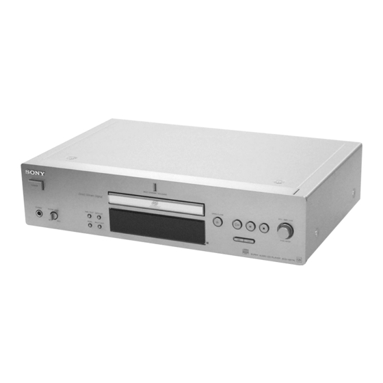
SCD-XB770 SECTION 2 This section is extracted from instruction manual. GENERAL Front Panel Parts Descriptions POWER OPEN CLOSE TIME/TEXT SACD/CD PHONES PHONE LEVEL PUSH ENTER MENU MULTI/2CH 1 POWER switch (14) 0 l AMS L dial (AMS: Automatic Music Sensor) -
Page 7: Remote Parts Descriptions
SCD-XB770 Remote Parts Descriptions 1 CONTINUE button (20) qs SACD/CD button (12) SHUFFLE button (20) qd MULTI/2CH button (12) PROGRAM button (21) qf ENTER button (24) 2 DISPLA Y MODE button (16) qg CLEAR button (21) 3 TIME/TEXT button (15) -
Page 8: Compatible Disc Types
SCD-XB770 Compatible Disc Types Classification by the channel configuration of the Super Audio CD 2 channel Super Audio CD Classification by the layer configuration Super Audio CD (single layer disc) 2 channel playback area Multi-channel Super Audio CD HD (Super Audio CD) -
Page 9: Disassembly
SCD-XB770 SECTION 3 DISASSEMBLY • This set can be disassembled in the order shown below. 3-1. DISASSEMBLY FLOW 3-2. COVER (Page 9) 3-3. FRONT PANEL SECTION 3-4. AUDIO BOARD, 3-5. MECHANISM DECK (Page 9) MAIN BOARD (CDM66B-DVBU6) (Page 10) (Page 10) 3-6. -
Page 10: Cover
SCD-XB770 Note: Follow the disassembly procedure in the numerical order given. 3-2. COVER 2 two flat head screws (TP) 3 cover 1 two screws 2 two flat head screws (TP) 4 two washers (DIA. 3.2) 5 two washers (P) 2 two flat head screws (TP) 4 two washers (DIA. -
Page 11: Audio Board, Main Board
SCD-XB770 3-4. AUDIO BOARD, MAIN BOARD 1 two wires (flat type) (19 core) (CN302, 303) 2 four connectors (CN301, 304, 305, 306) 8 wire (flat type) (12 core) (CN706) 8 wire (flat type) (30 core) (CN708) 7 AUDIO board 9 connector... -
Page 12: Base Unit (Dvbu-6)
SCD-XB770 3-6. BASE UNIT (DVBU-6) – BOTTOM VIEW – cam (66) base unit (DVBU-6) 3 base unit (DVBU-6) 1 screw (DIA. 12), floating... -
Page 13: Test Mode
SCD-XB770 Ver 1.1 2001.07 SECTION 4 TEST MODE This set automatically executes self-diagnosis and various checks Releasing Method of Test Mode [POWER] by entering the test mode. To release the test mode, turn the switch off. Note: This set automatically makes various adjustments according to the... - Page 14 SCD-XB770 Ver 1.1 2001.07 FOCUS command (2X): Focus related. (All servos must be already turned on (except command 21)) Name Description Remarks FSRCH ON/OFF The continuous vertical motion of the optical pick-up lens is turned on or Avoid a long-time use...
- Page 15 SCD-XB770 Ver 1.1 2001.07 TOOLS command (8X): Performs aging, reads adjusting parameters, etc. Name Description Remarks VERSION Firmware version is displayed Example: Ver 1.00 DISC AGING Not used for the servicing TRAY AGING Tray open-close aging is performed Number of times and eccentricity Not used for the servicing measurement Not used in this set.
- Page 16 SCD-XB770 Ver 1.1 2001.07 Set Check 92. SET CHECK SET TEST START 10. TOTAL CHECK 120. MANUAL CHK 0. IC&FL CHECK ? 11. AUTO CHECK ? 121. LOAD IN ? 1. TOTAL CHECK ? 12. MANUAL CHK ? 122. SPIN UP ? 2.
- Page 17 SCD-XB770 Ver 1.1 2001.07 4-1. IC AND FLUORESCENT DISPLAY TUBE CHECK Error display Causes (typical example) (SELF-DIAGNOSIS) PRAWN DRAM ERR 1. IC808 (D-RAM) is faulty The communication between microcomputer and main ICs (self- 2. IC801 (DSD decoder) is faulty diagnosis) and the fluorescent display tube all lit are checked.
- Page 18 SCD-XB770 Ver 1.1 2001.07 4-2. AUTO CHECK (AUTOMATIC VARIOUS MEASUREMENTS) The auto check is performed to check if the set operates stably. Though a checking is made automatically, whether the measured data are within the specification is evaluated by the service person. The auto check results in NG immediately, if the check itself causes an error.
- Page 19 SCD-XB770 Ver 1.1 2001.07 Items Description Remarks HENSHIN RYOU Eccentricity measurement For the CD only are measured Eccentricity (actual eccentric amount) of disc, disc pulley total • Read by dividing by 10 • 0 may be displayed if eccentricity is small (10um or less) (Due to...
- Page 20 SCD-XB770 Ver 1.1 2001.07 (2) CD (Use the test disc PATD-012 or YEDS-18) Note: Measured values in check items are typical ones. Check items Specified value LOAD IN TIME (msec) : 2108 1300 to 2000 SPIN UP TIME (msec) : 1354...
- Page 21 SCD-XB770 Ver 1.1 2001.07 4-3. SACD (DL) DISC OPERATION CHECK 4-4. HYBRID DISC OPERATION CHECK (• Perform as necessary) (• Perform as necessary) The stability of the set can be checked by repeating the combined This test checks the auto adjustment time required when the disc operation of focus jump (layer 0t1, layer 1t0) and access to is switched between HD (SACD) layer and CD layer.
- Page 22 SCD-XB770 Ver 1.1 2001.07 4-5 . AGING MODE 4-6. SHIPPING MODE (• Perform as necessary) The repaired set must be initialized, and for this purpose the set The aging can be performed to the set in the test mode. The aging should be set to the shipping mode.
- Page 23 SCD-XB770 Ver 1.1 2001.07 Error display is as follows. Error name, Disc type, IN SW (Sled in switch state), FOK (FOK signal state), LOCK (LOCK signal state), From (Displayed if effective), To (Displayed if effective), Aging times (Displayed in aging mode only)
- Page 24 SCD-XB770 Ver 1.1 2001.07 4-7. WAVEFORMS CHECK Traverse Check This set performs automatic adjustment for each disc, and there- Connection: fore the set need not be adjusted when parts are replaced, but it requires checking following the description in this section, 4-1.
- Page 25 SCD-XB770 Ver 1.1 2001.07 RF Level Check CLV Jitter Check (CD only) Checking and Connecting Location: Connection: Connection: – MAIN Board (Component Side) – oscilloscope oscilloscope MAIN board IC703 MAIN board TP704 (CH1) (AGND) TP703 TP516 (RFCK) TP506 TP504 TP703 (RFAC) –...
-
Page 26: Diagrams
SCD-XB770 Ver 1.1 2001.07 SECTION 5 DIAGRAMS 5-1. BLOCK DIAGRAM – RF/SERVO Section – ATOP DVDRFP INPUT PROGRAMMABLE RFAC RFAC BIAS, EQ FILTER (Page 27) RFSIN ATON DIFFERENTIATOR FULL WAVE RECTIFER AGCO • SIGNAL PATH : SACD PLAY CHARGE PUMP : CD PLAY CLAMP&... -
Page 27: Block Diagram - Servo Section
SCD-XB770 Ver 1.1 2001.07 5-2. BLOCK DIAGRAM – SERVO Section – RFAC D+3.3V (Page 28) FILTER DIGITAL SIGNAL PROCESSOR IC509 (2/2) 53 55 52 54 12 XTAO CLOCK 768FS (33.8688MHz) XTAI GENERATOR (Page 28) MDAT, BCLK, LRCK PCMD MDAT RFAC... -
Page 28: Block Diagram - Main Section
SCD-XB770 Ver 1.1 2001.07 5-3. BLOCK DIAGRAM – MAIN Section – SDATA, SCLK, SDEN • SIGNAL PATH (Page 26) : SACD PLAY FOK, MIRR, COUT, SCLK (Page 26) TE, FE (Page 26) ZMCKI, 256FS (Page 29) DSD DECODER LEVEL SHIFT... -
Page 29: Block Diagram - Audio Section
SCD-XB770 Ver 1.1 2001.07 5-4. BLOCK DIAGRAM – AUDIO Section – RV601 PHONES LEVEL HEADPHONE J601 R-CH DSD DIGITAL SIGNAL PROCESSOR PHONES IC308 IC803 DIGITAL FILTER, D/A CONVERTER DSL, DSR, MUTING IC301 Q403 DSLS, DSRS, DSC, DSLF, R-CH ANALOG J301... -
Page 30: Block Diagram - Display/Key Control/Power Supply Section
SCD-XB770 Ver 1.1 2001.07 5-5. BLOCK DIAGRAM – DISPLAY/KEY CONTROL/POWER SUPPLY Section – S830 ROTARY S807 – 809 ENCODER KEY0 S807 S808 S809 S801 – 805 RECT KEY1 MUTE +3.3V S801 S802 S803 D905, 906 D301 D302 MENU S804 S805... -
Page 31: Schematic Diagrams
SCD-XB770 5-6. NOTE FOR PRINTED WIRING BOARDS AND SCHEMATIC DIAGRAMS • Circuit Boards Location Note on Printed Wiring Board: Note on Schematic Diagram: POWER board • X : parts extracted from the component side. • All capacitors are in µF unless otherwise noted. pF: µµF •... -
Page 32: Schematic Diagram - Rf Board
SCD-XB770 5-7. SCHEMATIC DIAGRAM – RF Board – • • See page 48 for Waveforms. See page 51 for IC Block Diagram. CN005 AGND RFAC AGND C026 C039 C041 C036 0.01 0.01 MIRR C031 MIRR VMOD JL081 C040 VMOD C032 0.01... -
Page 33: Printed Wiring Boards - Rf/Loading Boards
SCD-XB770 5-8. PRINTED WIRING BOARDS – RF/LOADING Boards – • See page 31 for Circuit Boards Location. (SPINDLE) (SLED) (LIMIT) OPTICAL PICK-UP RF BOARD BLOCK KHM-230AAA (COMPONENT SIDE) MAIN BOARD CN708 (Page 34) 1-680-791- (11) RF BOARD LOADING BOARD (CONDUCTOR SIDE) -
Page 34: Main Board (Component Side)
SCD-XB770 5-9. PRINTED WIRING BOARD – MAIN Board (Component Side) – • See page 31 for Circuit Boards Location. • Semiconductor Location MAIN BOARD (COMPONENT SIDE) Ref. No. Location IC503 IC509 IC701 IC703 IC801 IC803 IC814 IC901 BOARD CN005 (Page 33) -
Page 35: Main Board (Conductor Side)
SCD-XB770 5-10. PRINTED WIRING BOARD – MAIN Board (Conductor Side) – • See page 31 for Circuit Boards Location. • Semiconductor Location MAIN BOARD Ref. No. Location (CONDUCTOR SIDE) D903 D904 IC502 IC504 IC512 H-10 IC702 IC706 IC708 IC802 IC808... -
Page 36: Schematic Diagram - Main (1/5)/ Loading Boards
SCD-XB770 5-11. SCHEMATIC DIAGRAM – MAIN (1/5)/LOADING Boards – • • See page 48 for Waveforms. See page 51 for IC Block Diagram. AGND (Page 39) DGND (Page TP501 DRVC (AGND) C592 M12V MGND C516 DSP_BUS CL502 TP517 CN708 (MNT3) -
Page 37: Schematic Diagram - Main Board (2/5)
SCD-XB770 5-12. SCHEMATIC DIAGRAM – MAIN Board (2/5) – • • See page 48 for Waveforms. See page 51 for IC Block Diagram. R545 100k C523 1500p R544 TP701 100k (JIT) D903 R729 JL1080 JL1081 1SS367 (2/2) SPINDLE MOTOR TP703... -
Page 38: Schematic Diagram - Main Board (3/5)
SCD-XB770 5-13. SCHEMATIC DIAGRAM – MAIN Board (3/5) – • See page 48 for Waveforms. CN704 CL1094 DGND C914 C795 DOUT CL1010 C842 C913 FL906 0.01 10V 0.01 6.3V CL1018 3.3VD A1IN CL1021 R803 CL883 A1OUT CL1023 (Page C796 R1025... -
Page 39: Schematic Diagram - Main Board (4/5)
SCD-XB770 5-14. SCHEMATIC DIAGRAM – MAIN Board (4/5) – • • See page 48 for Waveforms. See page 51 for IC Block Diagram. (Page 37) R912 FL901 R978 R913 R906 C916 C901 0.01 C906 R946 0.01 C902 0.01 EEPROM IC903... -
Page 40: Schematic Diagram - Main Board (5/5)
SCD-XB770 5-15. SCHEMATIC DIAGRAM – MAIN Board (5/5) – • See page 48 for Waveforms. (Page 38) CL810 XZLAT R1019 C917 CL807 0.01 CL811 HDMODESEL C912 0.01 CL804 CDMODE CL812 CL813 R996 CL814 FL904 R997 CL859 INVERTER CL815 CL858 IC802... -
Page 41: Schematic Diagram - Audio/Hp Boards
SCD-XB770 5-16. SCHEMATIC DIAGRAM – AUDIO/HP Boards – • • See page 48 for Waveforms. See page 51 for IC Block Diagram. D301 D302 1SS367-T3 1SS367-T3 Q301 DTA143TKA-T146 Q303 MUTING DTA143TKA-T146 CN301 CONTROL MUTING C333 R328 C334 2200 SWITCH CONTROL 4.7k... -
Page 42: Printed Wiring Board
SCD-XB770 5-17. PRINTED WIRING BOARD – AUDIO Board (Component Side) – • See page 31 for Circuit Boards Location. AUDIO BOARD (COMPONENT SIDE) (11) 1-681-002-... -
Page 43: Printed Wiring Boards - Audio (Conductor Side)/Hp Boards
SCD-XB770 5-18. PRINTED WIRING BOARDS – AUDIO (Conductor Side)/HP Boards – • See page 31 for Circuit Boards Location. J302 ANALOG 5.1CH OUT J301 J303 ANALOG DIGITAL (CD) IC309 2CH OUT FRONT SURR DIGITAL (CD) WOOFER CENTER COAXIAL AUDIO BOARD... -
Page 44: Printed Wiring Boards - Display/Key Boards
SCD-XB770 5-19. PRINTED WIRING BOARDS – DISPLAY/KEY Boards – • See page 31 for Circuit Boards Location. (Page 46) DISPLAY BOARD POWER BOARD CN905 FL801 FLUORESCENT INDICATOR TUBE S830 ROTARY A OPEN/CLOSE ENCODER l AMS L PUSH ENTER D803 1-681-006-... -
Page 45: Schematic Diagram - Display/Key Boards
SCD-XB770 5-20. SCHEMATIC DIAGRAM – DISPLAY/KEY Boards – • See page 48 for Waveforms. FL801 FLUORESCENT INDICATOR TUBE (Page 40) (Page 47) CNP802 CN801 Q801,802 SEGMENT GRID DRIVE DRIVE R819 R820 R821 2.2k 3.3k KEY0 R818 S807 S808 S809 REMOTE CONTROL... -
Page 46: Printed Wiring Boards - Power/Trans Boards
SCD-XB770 5-21. PRINTED WIRING BOARDS – POWER/TRANS Boards – • See page 31 for Circuit Boards Location. POWER BOARD TRANS BOARD AUDIO BOARD CN991 CN301 (Page 43) AUDIO BOARD (CHASSIS) CN306 (Page 43) L901 LINE FILTER T902 POWER T901 TRANSFORMER... -
Page 47: Schematic Diagram - Power/Trans Boards
SCD-XB770 5-22. SCHEMATIC DIAGRAM – POWER/TRANS Boards – CN905 R925 R924 R923 -33V T901 POWER L901 D922 Q921 C922 C921 C907 C906 TRANSFORMER (Page 45) UDZS-TE-17-9.1B 2SB1241TV2Q 0.033 0.033 D918 D917 LINE CN991 R922 100V 100V EC10DS2TE12L EC10DS2TE12L -33V REGULATOR FILTER 3.3k... - Page 48 SCD-XB770 Waveforms – MAIN Board – – RF Board – 1 IC001 el (TE) (SACD Play mode) 3 IC001 tj (RFAC) (SACD Play mode) 1 IC509 0 (WFCK), IC701 <zbz (WFCK) 4 IC509 ra (TE), IC901 yg (TE) 7 IC509 yj (BCK), IC701 <zb, (BCLK) qa IC701 <zzm (RFIN) (SACD Play mode)
- Page 49 SCD-XB770 qg IC801 tl (BCKAI) wg IC803 o; (LRCK) (CD Play mode) w; IC901 ra (EXTAL) 1.6 Vp-p 3.4 Vp-p 3.5 Vp-p 50 ns 177 ns 22.7 s qh IC801 ya (PHREFI) wh IC803 of (BCLK) (CD Play mode) wa IC803 wk (FS128) 3.5 Vp-p...
- Page 50 SCD-XB770 – AUDIO Board – – DISPLAY Board – 6 IC301 – 303 w; (DBCK) 1 IC304 1 1 IC801 t; (OSCO) 3.4 Vp-p 4 Vp-p 1.6 Vp-p 88.6 ns 354 ns 540 ns 7 IC301 – 303 qk (PSCK), ql (DSCK)
- Page 51 SCD-XB770 • IC Block Diagrams – RF Board – IC001 CXD1881R 64 63 62 61 60 59 55 54 53 52 FAST ATTACK INPUT OUTPUT HOLD FULL WAVE AGC CHARGE INHIBIT RECTIFER PUMP PROGRAMMABLE FROM S-PORT INPUT EQUALIZER DVDRFP FILTER...
-
Page 52: Main Board
SCD-XB770 – MAIN Board – IC509 CXD3068Q 59 58 57 56 55 54 53 52 51 50 49 48 47 46 45 44 43 42 41 DVDD2 ASYE DIGITAL ASYMMETRY CORRECTOR DIGITAL DOUT LRCK D/A DIGITAL PCMD INTERFACE DEMODULATOR TES1... - Page 53 SCD-XB770 IC701 CXD1882R-1 132131130129128 126125 123122 121120 119118 117116115114113112111110109108107 106105104103102101100 99 98 97 96 95 94 93 92 91 90 89 RF ASYMMETRY GNDA2 CONTROLLER MAIN DATA ECC & EDC PRIORITY RESOLVE GNDA1 & SEQUENSOR XRAS CD-ROM MDIN2 MAIN DATA MDIN1 ECC &...
- Page 54 SCD-XB770 – AUDIO Board – IC301 – 303 CXD9658N DBCK DSDL INTERFACE FILTER DSDR MULTI-LEVEL MULTI-LEVEL ANALOG DSCK DELTA-SIGMA LOW-PASS PSCK MODULATOR CONVERTER FILTER PBCK PDATA INTERFACE FILTER MODE PLRCK CONTROL ZEROR/ZEROA DGND POWER ZEROL/NA CONTROL VCOM VOUTL VOUTR AGND...
-
Page 55: Ic Pin Function Description
SCD-XB770 5-23. IC PIN FUNCTION DESCRIPTION MAIN BOARD IC509 CXD3068Q (DIGITAL SIGNAL PROCESSOR, DIGITAL SERVO PROCESSOR) Pin No. Pin Name Description DVDD0 — Power supply terminal (+3.3V) (digital system) XRST Reset signal input from the I/O expander (IC902) “L”: reset MUTE Muting on/off control signal input from the I/O expander (IC902) “H”: muting on... - Page 56 SCD-XB770 Pin No. Pin Name Description AVSS0 — Ground terminal (analog system) IGEN Stabilized current input for operational amplifiers AVDD0 — Power supply terminal (+3.3V) (analog system) ASYO EFM full-swing output terminal ASYI Asymmetry comparator voltage input terminal RFAC EFM signal input from the CXD1881R (IC001) AVSS1 —...
- Page 57 SCD-XB770 MAIN BOARD IC701 CXD1882R-1 (SACD DECODER) Pin No. Pin Name Description 1, 2 D5, D6 Two-way data bus with the CPU (IC901) and I/O expander (IC902) — Ground terminal (digital system) Two-way data bus with the CPU (IC901) and I/O expander (IC902) Address signal input from the CPU (IC901) —...
- Page 58 SCD-XB770 Pin No. Pin Name Description HINT Not used (pull up) XS16 Not used (pull up) Not used (fixed at “H” ) XPDI Not used (pull up) VDDS — Power supply terminal (+5V) (digital system) 59, 60 HA0, HA2 Not used (fixed at “H” ) —...
- Page 59 SCD-XB770 Pin No. Pin Name Description 118, 119 VCCA5, VCCA4 — Power supply terminal (+3.3V) (analog system) VCOR1 — VCO oscillating range setting resistor connected terminal VCOIN VCO input terminal 122, 123 GNDA4, GNDA3 — Ground terminal (analog system) LPF5 Signal output from the operation amplifier from PLL loop filter Middle point voltage (+1.65V) input terminal...
- Page 60 SCD-XB770 Pin No. Pin Name Description XTA1 System clock input terminal (33.8688 MHz) — Power supply terminal (+3.3V) (digital system) 172 to 176 D0 to D4 Two-way data bus with the CPU (IC901) and I/O expander (IC902)
- Page 61 SCD-XB770 MAIN BOARD IC801 CXD2752R (DSD DECODER) Pin No. Pin Name Description — Ground terminal (for core) XMSLAT Serial data latch pulse signal input from the CPU (IC901) MSCK Serial data transfer clock signal input from the CPU (IC901) MSDATI Serial data input from the CPU (IC901) —...
- Page 62 SCD-XB770 Pin No. Pin Name Description BCKAO Bit clock signal (2.8224 MHz) output terminal for DSD data output Not used (open) PHREFI Phase reference signal input for DSD output phase modulation from the CXD9647R (IC803) PHREFO Phase reference signal output terminal for DSD output phase modulation Not used (open)
- Page 63 SCD-XB770 Pin No. Pin Name Description WARFI Analog RF signal input for PSP physical disc mark detection from the CXD1881R (IC001) WAVRB A/D bottom reference terminal for PSP physical disc mark detection 128, 129 WAVSS — A/D ground terminal (for PSP physical disc mark detection) VSIO —...
- Page 64 SCD-XB770 MAIN BOARD IC803 CXD9647R (DSD DIGITAL SIGNAL PROCESSOR) Pin No. Pin Name Description — Power supply terminal (+3.3V) (digital system) XMSDOE Serial data output enable signal output terminal Not used (open) MSREADY Ready signal input from the CPU (IC901) “L”: ready...
- Page 65 SCD-XB770 Pin No. Pin Name Description — Power supply terminal (+3.3V) (digital system) DSAR DSD data (front R-ch) output to the digital filter (IC301) — Ground terminal (digital system) DSALS DSD data (surround L-ch) output to the digital filter (IC302) —...
- Page 66 SCD-XB770 MAIN BOARD IC901 CXP973F064-203R (CPU) Pin No. Pin Name Description SACD/CD mode selection signal output to the muting circuit MODE DF “L”: CD mode, “H”: SACD mode AMUTE Muting on/off signal output to the analog line circuit “L”: muting on...
- Page 67 SCD-XB770 Pin No. Pin Name Description SCK DSD Serial data transfer clock signal output to the DSD decoder (IC801) and CXD9647R (IC803) Laser diode on/off control signal output to the CXD1881R (IC001) LD ON “L”: laser diode off, “H”: laser diode on XDIS IO Reset signal output to the I/O expander (IC902) “L”: reset...
- Page 68 SCD-XB770 MAIN BOARD IC902 CXD1095BR (I/O EXPANDER) Pin No. Description Pin Name MUT CD Muting on/off control signal output to the CXD3068Q (IC509) “L”: muting on MUT 2D Muting control signal output to the BA5983FP (IC502) MUT LOAD Muting control signal output to the BA5912AFP (IC512)
- Page 69 SCD-XB770 Pin No. Pin Name Description — Power supply terminal (+3.3V) (digital system) 57, 58 — PA3, PA4 Not used (open) OUT SW Disc tray out detection signal input terminal Not used (fixed at “H”) — Not used (open) Detection signal input from limit in switch (S1) LIM SW The optical pick-up is inner position when “H”...
-
Page 70: Exploded Views
SCD-XB770 SECTION 6 EXPLODED VIEWS NOTE: • -XX and -X mean standardized parts, so they • Items marked “*” are not stocked since they The components identified by mark 0 or dotted line with mark may have some difference from the original are seldom required for routine service. -
Page 71: Front Panel Section
1-681-008-11 HP BOARD 3-354-931-01 KNOB (DIA. 10) (BLACK) 1-681-009-11 KEY BOARD 3-354-931-41 KNOB (DIA. 10) (SILVER) 4-232-616-01 BUTTON (TIME/TEXT) (BLACK) 4-942-568-41 EMBLEM (NO.5), SONY (BLACK) 4-232-616-11 BUTTON (TIME/TEXT) (SILVER) 4-942-568-61 EMBLEM (NO.5), SONY (SILVER) 4-228-512-01 BUTTON (SUB) (BLACK) 4-232-609-01 PANEL, FRONT (BLACK) -
Page 72: Chassis Section
SCD-XB770 6-3. CHASSIS SECTION CDM66B-DVBU6 supplied not supplied not supplied not supplied not supplied not supplied not supplied T902 T901 not supplied not supplied not supplied not supplied not supplied not supplied not supplied The components identified by mark 0 or dotted line with mark 0 are critical for safety. -
Page 73: Mechanism Deck Section (Cdm66B-Dvbu6)
SCD-XB770 6-4. MECHANISM DECK SECTION (CDM66B-DVBU6) not supplied not supplied DVBU-6 M151 Ref. No. Part No. Description Remark Ref. No. Part No. Description Remark 4-231-530-01 TRAY (66) 3-053-844-01 YOKE 4-232-682-01 CUSHION (66) 4-231-529-01 CHASSIS (66) 4-232-712-01 CAM (66) 4-227-899-01 SCREW (DIA. 12), FLOATING... -
Page 74: Base Unit Section (Dvbu-6)
SCD-XB770 6-5. BASE UNIT SECTION (DVBU-6) not supplied not supplied The components identified by mark 0 or dotted line with mark 0 are critical for safety. Replace only with part number specified. Ref. No. Part No. Description Remark Ref. No. -
Page 75: Electrical Parts List
SCD-XB770 SECTION 7 ELECTRICAL PARTS LIST AC SW AUDIO NOTE: • Due to standardization, replacements in the • Items marked “*” are not stocked since they The components identified by mark 0 or dotted line with mark parts list may be different from the parts speci- are seldom required for routine service. - Page 76 SCD-XB770 AUDIO Ref. No. Part No. Description Remark Ref. No. Part No. Description Remark C506 1-162-927-11 CERAMIC CHIP 100PF L303 1-216-813-11 METAL CHIP 1/16W C507 1-162-927-11 CERAMIC CHIP 100PF L304 1-216-813-11 METAL CHIP 1/16W C508 1-162-970-11 CERAMIC CHIP 0.01uF L305...
- Page 77 SCD-XB770 AUDIO DISPLAY Ref. No. Part No. Description Remark Ref. No. Part No. Description Remark R511 1-259-983-11 CARBON MELF 1/8W R328 1-216-829-11 METAL CHIP 4.7K 1/16W R512 1-216-829-11 METAL CHIP 4.7K 1/16W R329 1-216-801-11 METAL CHIP 1/16W R513 1-216-849-11 METAL CHIP...
- Page 78 SCD-XB770 DISPLAY LOADING MAIN Ref. No. Part No. Description Remark Ref. No. Part No. Description Remark < CONNECTOR > < JACK > CN801 1-779-549-21 CONNECTOR, FFC (LIF (NON-ZIF)) 12P J601 1-770-307-11 JACK (LARGE TYPE) (PHONES) < LED > < NOISE FILTER/RESISTOR >...
- Page 79 SCD-XB770 MAIN Ref. No. Part No. Description Remark Ref. No. Part No. Description Remark C523 1-162-965-11 CERAMIC CHIP 0.0015uF 10% C707 1-162-921-11 CERAMIC CHIP 33PF C525 1-107-826-11 CERAMIC CHIP 0.1uF C708 1-162-964-11 CERAMIC CHIP 0.001uF C709 1-164-156-11 CERAMIC CHIP 0.1uF...
- Page 80 SCD-XB770 MAIN Ref. No. Part No. Description Remark Ref. No. Part No. Description Remark C794 1-126-246-11 ELECT CHIP 220uF C911 1-125-822-11 TANTALUM 10uF C795 1-126-206-11 ELECT CHIP 100uF 6.3V C912 1-162-970-11 CERAMIC CHIP 0.01uF C913 1-162-970-11 CERAMIC CHIP 0.01uF C796...
- Page 81 SCD-XB770 MAIN Ref. No. Part No. Description Remark Ref. No. Part No. Description Remark IC703 8-759-701-40 IC NJM3404AM-T1 FB707 1-500-283-11 FERRITE IC706 8-759-543-83 IC KM416V1204CT-L6 FB708 1-500-283-11 FERRITE IC708 8-759-701-40 IC NJM3404AM-T1 FB709 1-500-283-11 FERRITE FB710 1-500-283-11 FERRITE IC801 8-752-407-50 IC CXD2752R...
- Page 82 SCD-XB770 MAIN Ref. No. Part No. Description Remark Ref. No. Part No. Description Remark R558 1-216-841-11 METAL CHIP 1/16W R660 1-218-700-11 METAL CHIP 2.2K 0.5% 1/16W R559 1-216-797-11 METAL CHIP 1/16W R560 1-216-821-11 METAL CHIP 1/16W R661 1-216-296-11 SHORT R561...
- Page 83 SCD-XB770 MAIN Ref. No. Part No. Description Remark Ref. No. Part No. Description Remark R768 1-216-809-11 METAL CHIP 1/16W R885 1-216-833-11 METAL CHIP 1/16W R769 1-218-700-11 METAL CHIP 2.2K 0.5% 1/16W R770 1-216-864-11 METAL CHIP 1/16W R886 1-216-833-11 METAL CHIP...
- Page 84 SCD-XB770 MAIN POWER Ref. No. Part No. Description Remark Ref. No. Part No. Description Remark R951 1-216-821-11 METAL CHIP 1/16W R952 1-216-827-11 METAL CHIP 3.3K 1/16W A-4725-671-A POWER BOARD, COMPLETE R953 1-216-833-11 METAL CHIP 1/16W *********************** R954 1-216-833-11 METAL CHIP...
- Page 85 SCD-XB770 POWER Ref. No. Part No. Description Remark Ref. No. Part No. Description Remark D916 8-719-210-39 DIODE EC10QS-04 C012 1-164-172-11 CERAMIC CHIP 0.0056uF 10% D917 8-719-210-33 DIODE EC10DS2 C013 1-164-172-11 CERAMIC CHIP 0.0056uF 10% D918 8-719-210-33 DIODE EC10DS2 C015 1-117-370-11 CERAMIC CHIP...
- Page 86 SCD-XB770 TRANS Ref. No. Part No. Description Remark Ref. No. Part No. Description Remark < TRANSISTOR > < LINE FILTER > Q001 8-729-805-25 TRANSISTOR 2SB1121-S 0 L901 1-424-485-11 FILTER, LINE Q002 8-729-805-25 TRANSISTOR 2SB1121-S *********************************************************** Q003 8-729-805-25 TRANSISTOR 2SB1121-S Q005...
- Page 87 SCD-XB770 MEMO...
-
Page 88: Revision History
SCD-XB770 REVISION HISTORY Clicking the version allows you to jump to the revised page. Also, clicking the version at the upper right on the revised page allows you to jump to the next revised page. Ver. Date Description of Revision 2001.07...