Table of Contents
Advertisement
QQ
3 7 63 1515 0
SERVICE MANUAL
Ver 1.0 2003.04
TE
L 13942296513
When a super audio CD is played
Playing frequency range 2 Hz to 100 kHz
Frequency response
2 Hz to 50 kHz (–3 dB)
Dynamic range
104 dB or more
Total harmonic distortion rate
0.0018 % or less
Wow and flutter
Value of measurable limit (±0.001 %
W. PEAK) or less
When a CD is played
Frequency response
2 Hz to 20 kHz
Dynamic range
99 dB or more
Total harmonic distortion rate
0.002 % or less
Wow and flutter
Value of measurable limit (±0.001 %
W. PEAK) or less
www
.
Sony Corporation
9-877-171-01
2003D0500-1
Home Audio Company
C 2003.04
Published by Sony Engineering Corporation
http://www.xiaoyu163.com
Output connector
ANALOG OUT
DIGITAL (CD)
OUT
OPTICAL*
DIGITAL (CD)
OUT
COAXIAL*
PHONES
*Output only the audio signals of the CD
x
ao
u163
y
i
http://www.xiaoyu163.com
SCD-XB790
2 9
8
Model Name Using Similar Mechanism
CD Mechanism Type
Base Unit Name
Optical Pick-up Name
SPECIFICATIONS
Q Q
3
6 7
1 3
1 5
Load impedance
Jack type
Output level
Over 10 kilohms
Phono
2 Vrms
jacks
(at 50 kilohms)
Square
–18 dBm
Light emitting
(
)
optical
wave length:
output
660 nm
connector
Coaxial
75 ohms
0.5 Vp-p
output
connector
Stereo
32 ohms
10 mW
phone jack
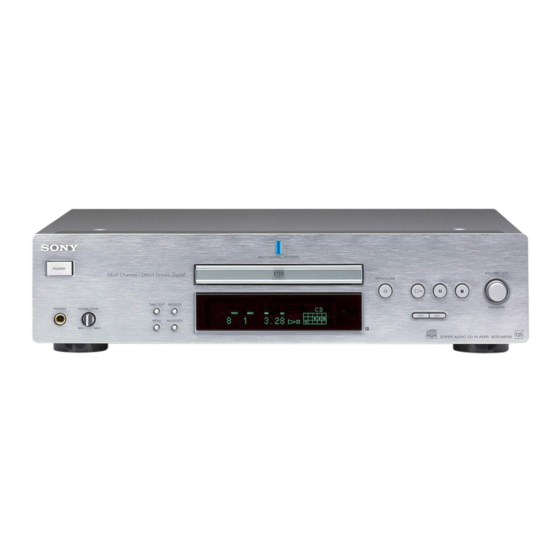
SUPER AUDIO CD PLAYER
co
.
9 4
2 8
AEP Model
UK Model
SCD-XB780
CDM66B-DVBU6B
DVBU-6B
KHM-234AMA
0 5
8
2 9
9 4
2 8
General
Laser
Semiconductor laser
(Super Audio CD: λ = 650 nm)
(CD: λ = 780 nm)
Emission duration: continuous
Laser radiant power:
5.47 uW at 650 nm
*These output is the value measured at a distance of about
200mm from the objective lens surface on the optical pick-up.
Power requirements
230 V AC, 50/60 Hz
Power consumption
25 W
430 × 111 × 283 mm incl. projecting
Dimensions (w/h/d)
parts
Mass (approx.)
5.8 kg
Supplied accessories
• Audio connecting cord
Stereo cable (1)
•Remote commander RM-SX700 (1)
• R06 (size-AA) batteries (2)
Design and specifications are subject to change without notice.
m
9 9
9 9
Advertisement
Table of Contents

Related Manuals for Sony SCD-XB790


Summary of Contents for Sony SCD-XB790
- Page 1 Stereo cable (1) •Remote commander RM-SX700 (1) • R06 (size-AA) batteries (2) Design and specifications are subject to change without notice. SUPER AUDIO CD PLAYER u163 Sony Corporation 9-877-171-01 2003D0500-1 Home Audio Company C 2003.04 Published by Sony Engineering Corporation http://www.xiaoyu163.com...
-
Page 2: Table Of Contents
LINE WITH MARK 0 ON THE SCHEMATIC DIAGRAMS AND IN THE PARTS LIST ARE CRITICAL TO SAFE OPERATION. REPLACE THESE COMPONENTS WITH SONY PARTS WHOSE PART NUMBERS APPEAR AS SHOWN IN THIS MANUAL OR IN SUPPLEMENTS PUB- LISHED BY SONY. -
Page 3: Servicing Notes
SCD-XB790 SECTION 1 SERVICING NOTES 3 7 63 1515 0 NOTES ON HANDLING THE OPTICAL PICK-UP BLOCK OR BASE UNIT The laser diode in the optical pick-up block may suffer electro- static break-down because of the potential difference generated by the charged electrostatic load, etc. - Page 4 SCD-XB790 3 7 63 1515 0 DISPLAY BOARD SERVICE POSITION In checking the DISPLAY board, prepare jig (extension cable J-2501-200-A : 1.00 mm Pitch, 11 cores, Length 300 mm.) MAIN board CN706 DISPLAY board Connect jig (extension cable J-2501-200-A) to the DISPLAY board (CN801) and MAIN board (CN706).
- Page 5 SCD-XB790 3 7 63 1515 0 RESETTING OPERATION AT POWER ON If the power is turned on with a disc loaded in the set, a sequence of operation as shown below will be performed. (The operation varies depending on the type of disc) Condition: continue mode...
-
Page 6: General
SCD-XB790 SECTION 2 This section is extracted from instruction manual. 3 7 63 1515 0 GENERAL Front Panel Parts Descriptions POWER OPEN CLOSE TIME/TEXT SACD/CD PHONES PHONE LEVEL PUSH ENTER MENU MULTI/2CH 1 POWER switch 6 A OPEN/CLOSE button qs PHONE LEVEL Press to turn on the player. -
Page 7: Remote Parts Descriptions
SCD-XB790 3 7 63 1515 0 Remote Parts Descriptions 1 CONTINUE button qs SACD/CD button Press to resume normal play from Shuffle Play or Each time you press the button while playing back a Programme Play. hybrid disc, the layer to be played back switches... -
Page 8: Disassembly
SCD-XB790 SECTION 3 DISASSEMBLY 3 7 63 1515 0 • This set can be disassembled in the order shown below. 3-1. DISASSEMBLY FLOW 3-2. CASE (Page 9) 3-3. FRONT PANEL SECTION 3-4. AUDIO BOARD, 3-5. MECHANISM DECK MAIN BOARD... -
Page 9: Case
SCD-XB790 3 7 63 1515 0 Note: Follow the disassembly procedure in the numerical order given. 3-2. CASE 2 two flat head screws (TP) 3 case 1 two screws 2 two flat head screws (TP) 2 two flat head screws (TP) L 13942296513 3-3. -
Page 10: Audio Board, Main Board
SCD-XB790 3 7 63 1515 0 3-4. AUDIO BOARD, MAIN BOARD 1 two wires (flat type) (19 core) (CN302, 303) 2 four connectors (CN301, 304, 305, 306) 8 wire (flat type) (11 core) (CN706) 8 wire (flat type) (30 core) (CN708) -
Page 11: Base Unit (Dvbu-6B)
SCD-XB790 3 7 63 1515 0 3-6. BASE UNIT (DVBU-6B) – BOTTOM VIEW – cam (66) base unit (DVBU-6B) 3 base unit (DVBU-6B) 1 screw (DIA. 12), floating L 13942296513 u163 http://www.xiaoyu163.com... -
Page 12: Test Mode
SCD-XB790 SECTION 4 TEST MODE 3 7 63 1515 0 Setting Method of Test Mode In this set, various checks are automatically performed by executing [POWER] the commands in the test mode. Turn the button on while pressing the... - Page 13 SCD-XB790 3 7 63 1515 0 TRACKING command (4X): Tracking servo related. Name Description Remarks TGAIN NM/UP The tracking servo gain is switched between normal and up Normal or up are switched alternately ADJ TRK DSP The traverse AGC and E-F balance adjustment is performed...
- Page 14 SCD-XB790 3 7 63 1515 0 How to Apply Servo by Manual Operation Error display Causes (typical example) In analyzing failures of the set, the servo may be applied by manual EEPROM ERROR 1. IC903 (EEPROM) is faulty operation. To apply servo in the test mode, use the following SAMBA DRAM ERR 1.
- Page 15 SCD-XB790 3 7 63 1515 0 4-3. SET CHECK (AUTOMATIC VARIOUS MEASUREMENTS) The operational stability of the set is checked. The check and OK/NG judgment are performed automatically. Note: In the set check using the CD, besides a checking, the MIRR time used for the disc check is measured every optical pick-up, and from the measured result, the threshold value is calculated and it is stored in the EEPROM (IC903) on the MAIN board.
- Page 16 SCD-XB790 3 7 63 1515 0 Specified Value: Specified value used for OK/NG judgment when executing 92. SET CHECKtAUTO CHECK SP? Measured Items Specified value RF AVRG (ADJ) 8Ch to ABh VC AVRG (ADJ) 1F7h to09h (1) CD 1EEh to 12h...
- Page 17 SCD-XB790 3 7 63 1515 0 4-4. SACD (DL) DISC OPERATION CHECK 4-6. WAVEFORMS CHECK BU Electrical Adjustment Mode (• Perform as necessary) This checking performs the focus jump using a DL disc, which is The BU electrical adjustment mode is used to check the S curve a dual-layer HD disc, to verify the stability of the set.
- Page 18 SCD-XB790 3 7 63 1515 0 Traverse Check RF Level Check Connection: Connection: oscilloscope oscilloscope MAIN board MAIN board TP703 (RFAC) TP513 (TE) – TP704 (AGND) – TP504 (AVC) Checking Method: Checking Method: 1. Under the condition of S curve waveform check mode in step 1.
- Page 19 SCD-XB790 3 7 6 3 1 5 1 5 0 CLV Jitter Check (CD only) Connection: oscilloscope MAIN board (CH1) TP516 (RFCK) – TP517(WFCK) (CH2) TP808 (DG) Checking Method: Under the condition of RF level check mode in step 3, connect the...
-
Page 20: Diagrams
SCD-XB790 SECTION 5 3 7 6 3 1 5 1 5 0 DIAGRAMS 5-1. BLOCK DIAGRAM – RF/SERVO Section – DVDRFP ATON INPUT PROGRAMMABLE RFAC RFAC BIAS, EQ FILTER (Page 21) RFSIN ATOP DIFFERENTIATOR FULL WAVE RECTIFER • SIGNAL PATH... -
Page 21: Block Diagram - Servo Section
SCD-XB790 3 7 6 3 1 5 1 5 0 5-2. BLOCK DIAGRAM – SERVO Section – RFAC D+3.3V (Page 22) FILTER DIGITAL SIGNAL PROCESSOR IC509 (2/2) 53 55 52 54 12 XTAO CLOCK XTAI 768FS (33.8688MHz) GENERATOR (Page 22) -
Page 22: Block Diagram - Main Section
SCD-XB790 3 7 6 3 1 5 1 5 0 5-3. BLOCK DIAGRAM – MAIN Section – SDATA, SCLK, SDEN • SIGNAL PATH (Page 20) : SACD PLAY FOK, MIRR, COUT, SCLK (Page 20) TE, FE, PI (Page 20) -
Page 23: Block Diagram - Audio Section
SCD-XB790 3 7 6 3 1 5 1 5 0 5-4. BLOCK DIAGRAM – AUDIO Section – RV601 PHONE LEVEL HEADPHONE J601 R-CH PHONES IC308 (1/2) SDATAL, SDATR, MUTING SDATALS, SDATARS, Q403 SDATAC, SDATALF, 64FS ANALOG J301 SDATAL DSD1... -
Page 24: Block Diagram - Display/Key Control/Power Supply Section
SCD-XB790 3 7 6 3 1 5 1 5 0 5-5. BLOCK DIAGRAM – DISPLAY/KEY CONTROL/POWER SUPPLY Section – S810 – 813 KEY0 S801 – 806 D301 D302 RECT D905, 906 S830 KEY1 ROTARY ENCODER +3.3V +3.3V REGULATOR IC302... -
Page 25: Schematic Diagrams
SCD-XB790 3 7 6 3 1 5 1 5 0 5-6. NOTE FOR PRINTED WIRING BOARDS AND SCHEMATIC DIAGRAMS • Circuit Boards Location Note on Printed Wiring Board: Note on Schematic Diagram: POWER board • X : parts extracted from the component side. -
Page 26: Schematic Diagram - Rf Board
SCD-XB790 3 7 6 3 1 5 1 5 0 5-7. SCHEMATIC DIAGRAM – RF Board – • • See page 42 for Waveforms. See page 45 for IC Block Diagram. CN005 C036 C045 AGND 1000p RFAC AGND Q004... -
Page 27: Printed Wiring Boards - Rf/Loading Boards
SCD-XB790 3 7 6 3 1 5 1 5 0 5-8. PRINTED WIRING BOARDS – RF/LOADING Boards – • See page 25 for Circuit Boards Location. (SPINDLE) (SLED) (LIMIT) OPTICAL PICK-UP RF BOARD BLOCK KHM-234AMA (COMPONENT SIDE) MAIN BOARD... -
Page 28: Printed Wiring Board - Main Board (Component Side)
SCD-XB790 3 7 6 3 1 5 1 5 0 5-9. PRINTED WIRING BOARD – MAIN Board (Component Side) – • See page 25 for Circuit Boards Location. • Semiconductor Location Ref. No. Location MAIN BOARD (COMPONENT SIDE) IC501... -
Page 29: Main Board (Conductor Side)
SCD-XB790 3 7 6 3 1 5 1 5 0 5-10. PRINTED WIRING BOARD – MAIN Board (Conductor Side) – • See page 25 for Circuit Boards Location. • Semiconductor Location MAIN BOARD (CONDUCTOR SIDE) Ref. No. Location D903... -
Page 30: Schematic Diagram - Main (1/5)/Loading Boards
SCD-XB790 3 7 6 3 1 5 1 5 0 5-11. SCHEMATIC DIAGRAM – MAIN (1/5)/LOADING Boards – • • See page 42 for Waveforms. See page 45 for IC Block Diagram. (Page 34) (1/5) AGND DGND DRVC (Page 34) -
Page 31: Schematic Diagram - Main Board (2/5)
SCD-XB790 3 7 6 3 1 5 1 5 0 5-12. SCHEMATIC DIAGRAM – MAIN Board (2/5) – (Page 30) (2/5) C587 C520 22 16V C525 JL617 JL618 +2.5V REGULATOR JL528 IC504 µPC2905T-E1 TRACKING R554 C527 R632 R606 2.7k... -
Page 32: Schematic Diagram - Main Board (3/5)
SCD-XB790 3 7 6 3 1 5 1 5 0 5-13. SCHEMATIC DIAGRAM – MAIN Board (3/5) – • • See page 42 for Waveforms. See page 45 for IC Block Diagram. (3/5) R729 IC706 TP701 (2/2) (2/2) (1/2) -
Page 33: Schematic Diagram - Main Board (4/5)
SCD-XB790 3 7 6 3 1 5 1 5 0 5-14. SCHEMATIC DIAGRAM – MAIN Board (4/5) – • See page 42 for Waveforms. (4/5) +2.5V REGULATOR IC702 C795 TA48M025F 6.3V TP807 R810 C870 C842 0.033 0.01 R809 C796... -
Page 34: Schematic Diagram - Main Board (5/5)
SCD-XB790 3 7 6 3 1 5 1 5 0 5-15. SCHEMATIC DIAGRAM – MAIN Board (5/5) – • • See page 42 for Waveforms. See page 45 for IC Block Diagram. (Page 32) (Page 33) (5/5) R1007 R928... -
Page 35: Schematic Diagram - Audio/Hp Boards
SCD-XB790 3 7 6 3 1 5 1 5 0 5-16. SCHEMATIC DIAGRAM – AUDIO/HP Boards – • • See page 42 for Waveforms. See page 45 for IC Block Diagram. D311 1SS367-T3 CN301 D312 IC302 D301 D302 1SS367-T3... -
Page 36: Printed Wiring Board
SCD-XB790 3 7 6 3 1 5 1 5 0 5-17. PRINTED WIRING BOARD – AUDIO Board (Component Side) – • See page 25 for Circuit Boards Location. AUDIO BOARD (COMPONENT SIDE) 1 3 9 4 2 2 9 6 5 1 3... -
Page 37: Printed Wiring Boards - Audio (Conductor Side)/Hp Boards
SCD-XB790 3 7 6 3 1 5 1 5 0 5-18. PRINTED WIRING BOARDS – AUDIO (Conductor Side)/HP Boards – • See page 25 for Circuit Boards Location. • Semiconductor Location Ref. No. Location J302 ANALOG D301 J301 5.1CH OUT... -
Page 38: Printed Wiring Boards - Display/Key Boards
SCD-XB790 3 7 6 3 1 5 1 5 0 5-19. PRINTED WIRING BOARDS – DISPLAY/KEY Boards – • See page 25 for Circuit Boards Location. POWER BOARD KEY BOARD DISPLAY BOARD (Page 40) CN905 1 64 NO810 MENU... -
Page 39: Schematic Diagram - Display/Key Boards
SCD-XB790 3 7 6 3 1 5 1 5 0 5-20. SCHEMATIC DIAGRAM – DISPLAY/KEY Boards – • See page 42 for Waveforms. FL801 FLUORESCENT INDICATOR TUBE CN802 -33V +3.3V (Page 41) R812 R813 R814 R815 2.2k 4.7k Q803... -
Page 40: Printed Wiring Boards - Power/Power Sw/Pt Boards
SCD-XB790 3 7 6 3 1 5 1 5 0 5-21. PRINTED WIRING BOARDS – POWER/POWER SW/PT Boards – • See page 25 for Circuit Boards Location. POWER BOARD PT BOARD IC903 IC901 AUDIO BOARD CN301 (Page 37) CN991 ∗... -
Page 41: Schematic Diagram - Power/Power Sw/Pt Boards
SCD-XB790 3 7 6 3 1 5 1 5 0 5-22. SCHEMATIC DIAGRAM – POWER/POWER SW/PT Boards – CN905 +3.3V T901 POWER TRANSFORMER L901 -33V CN991 R924 R923 R925 Q921 LINE FILTER 2SB1241-Q-TV2 C922 C921 C907 C906 C923 D918... - Page 42 SCD-XB790 3 7 6 3 1 5 1 5 0 • Waveforms – MAIN Board – – RF Board – qa IC509 0 (WFCK), IC701 <zbz (WFCK) 1 IC001 el (TE) (SACD Play mode) 3 IC001 tj (RFAC) (SACD Play mode) qf IC509 ra (TE), IC901 yg (TE) qh IC509 yg (LRCK), IC701 <znc (LRCK)
- Page 43 SCD-XB790 3 7 63 1515 0 – AUDIO Board – wd IC801 qa (MCKI), IC811 qs wj IC901 ra (EXTAL) ea IC304 1 2.5 Vp-p 1.4 Vp-p 2.5 Vp-p 29.5 ns 50 ns 88.6 ns wf IC801 tl (BCKAI), IC904 4 (FS128) es IC304 4, IC301 ed (PSCK), ef (DSCK) 3.4 Vp-p...
- Page 44 SCD-XB790 3 7 63 1515 0 – DISPLAY Board – eg IC301 ta (PLRCK) (CD Play mode) ra IC801 t; (OSCO) 3.4 Vp-p 1.6 Vp-p 22.7 µs 540 ns rs IC801 ta (OSCI) 3.8 Vp-p 452 ns L 13942296513 u163 http://www.xiaoyu163.com...
- Page 45 SCD-XB790 3 7 63 1515 0 • IC Block Diagrams – RF Board – IC001 CXD1881AR-2 64 63 62 61 60 59 55 54 53 52 FAST ATTACK INPUT OUTPUT HOLD FULL WAVE AGC CHARGE INHIBIT RECTIFER PUMP PROGRAMMABLE...
- Page 46 SCD-XB790 3 7 63 1515 0 – MAIN Board – IC509 CXD3068Q 59 58 57 56 55 54 53 52 51 50 49 48 47 46 45 44 43 42 41 DVDD2 ASYE DIGITAL ASYMMETRY CORRECTOR DIGITAL DOUT LRCK...
- Page 47 SCD-XB790 3 7 63 1515 0 IC701 CXD1882R-1 132131130129128 126125 123122 121120 119118 117116115114113112111110109108107 106105104103102101100 99 98 97 96 95 94 93 92 91 90 89 RF ASYMMETRY GNDA2 CONTROLLER MAIN DATA PRIORITY RESOLVE ECC & EDC GNDA1 & SEQUENSOR...
- Page 48 SCD-XB790 3 7 63 1515 0 – AUDIO Board – IC301 CXD9709Q 26 VCOM2 SYSTEM OUTPUT AMP & OUTPUT AMP & OUTPUT AMP & OUTPUT AMP & CLOCK LOW-PASS FILTER LOW-PASS FILTER LOW-PASS FILTER LOW-PASS FILTER SYSTEM CLOCK CONVERTER...
-
Page 49: Ic Pin Function Description
SCD-XB790 5-23. IC PIN FUNCTION DESCRIPTION 3 7 63 1515 0 • MAIN BOARD IC509 CXD3068Q (DIGITAL SIGNAL PROCESSOR, DIGITAL SERVO PROCESSOR) Pin No. Pin Name Description DVDD0 — Power supply terminal (+3.3V) (digital system) XRST Reset signal input from the programmable logic device “L”: reset... - Page 50 SCD-XB790 3 7 63 1515 0 Pin No. Pin Name Description AVDD0 — Power supply terminal (+3.3V) (analog system) ASYO EFM full-swing output terminal ASYI Asymmetry comparator voltage input terminal RFAC EFM signal input from the SACD/CD RF amplifier AVSS1 —...
- Page 51 SCD-XB790 3 7 63 1515 0 • MAIN BOARD IC701 CXD1882R-1 (SACD DECODER) Pin No. Pin Name Description 1, 2 D5, D6 Two-way data bus with the CPU and programmable logic device — Ground terminal (digital system) Two-way data bus with the CPU and programmable logic device Address signal input from the CPU —...
- Page 52 SCD-XB790 3 7 63 1515 0 Pin No. Pin Name Description HINT Not used XS16 Not used Not used XPDI Not used VDDS — Power supply terminal (+5V) (digital system) 59, 60 HA0, HA2 Not used — Ground terminal (digital system)
- Page 53 SCD-XB790 3 7 63 1515 0 Pin No. Pin Name Description VCOR1 — VCO oscillating range setting resistor connected terminal VCOIN VCO input terminal 122, 123 GNDA4, GNDA3 — Ground terminal (analog system) LPF5 Signal output from the operation amplifier from PLL loop filter Middle point voltage (+1.65V) input terminal...
- Page 54 SCD-XB790 3 7 63 1515 0 Pin No. Pin Name Description — Power supply terminal (+3.3V) (digital system) 172 to 176 D0 to D4 Two-way data bus with the CPU and programmable logic device L 13942296513 u163 http://www.xiaoyu163.com...
- Page 55 SCD-XB790 3 7 63 1515 0 • MAIN BOARD IC801 CXD2753R (DSD DECODER) Pin No. Pin Name Description — Ground terminal (for core) XMSLAT Serial data latch pulse signal input from the CPU MSCK Serial data transfer clock signal input from the CPU...
- Page 56 SCD-XB790 3 7 63 1515 0 Pin No. Pin Name Description BCKAO Bit clock signal (2.8224 MHz) output terminal for DSD data output Not used PHREFI Clock signal (2.8224 MHz) input from the programmable logic device PHREFO Phase reference signal output terminal for DSD output phase modulation Not used...
- Page 57 SCD-XB790 3 7 63 1515 0 Pin No. Pin Name Description Operation clock signal input for PSP physical disc mark detection from the SACD decoder 124, 125 WAVDD — A/D power supply terminal (+2.5V) (for PSP physical disc mark detection)
- Page 58 SCD-XB790 3 7 63 1515 0 • MAIN BOARD IC901 CXP973064-227R (CPU) Pin No. Pin Name Description MUT LOAD Muting on/off control signal output to the loading motor drive “H”: muting on AMUTE Analog muting control signal output terminal Not used...
- Page 59 SCD-XB790 3 7 63 1515 0 Pin No. Pin Name Description FLOUT Serial data output to the fluorescent indicator tube driver FLCLK Serial data transfer clock signal output to the fluorescent indicator tube driver — Ground terminal (digital system)
- Page 60 SCD-XB790 3 7 63 1515 0 • MAIN BOARD IC904 ISPLSI2032VE-110LT44-SA (PROGRAMMABLE LOGIC DEVICE) Pin No. Description Pin Name TRKSW Tracking coil drive on/off control signal output “H”: drive on ZEROL L-ch zero data flag detection signal input from the digital filter FS64 Clock signal (2.8224 MHz) output to the digital filter and DSD decoder...
-
Page 61: Exploded Views
SCD-XB790 SECTION 6 EXPLODED VIEWS 3 7 63 1515 0 NOTE: • Items marked “*” are not stocked since they • -XX and -X mean standardized parts, so they The components identified by mark 0 or dotted line with mark may have some difference from the original are seldom required for routine service. -
Page 62: Front Panel Section
3-354-931-01 KNOB (DIA. 10) (BLACK) 4-232-616-01 BUTTON (TIME/TEXT) (BLACK) 3-354-931-61 KNOB (DIA. 10) (SILVER) 4-232-616-31 BUTTON (TIME/TEXT) (SILVER) 4-942-568-41 EMBLEM (NO.5), SONY (BLACK) 4-228-512-01 BUTTON (SUB) (BLACK) 4-942-568-61 EMBLEM (NO.5), SONY (SILVER) 4-228-512-31 BUTTON (SUB) (SILVER) 4-244-275-01 PANEL, FRONT (BLACK) -
Page 63: Chassis Section
SCD-XB790 3 7 63 1515 0 6-3. CHASSIS SECTION mechanism deck section (CDM66B-DVBU6B) supplied not supplied not supplied not supplied not supplied not supplied not supplied not supplied T902 T901 L 13942296513 not supplied not supplied not supplied not supplied... -
Page 64: Mechanism Deck Section (Cdm66B-Dvbu6B)
SCD-XB790 3 7 63 1515 0 6-4. MECHANISM DECK SECTION (CDM66B-DVBU6B) not supplied not supplied base unit section (DVBU-6B) L 13942296513 M151 Ref. No. Part No. Description Remark Ref. No. Part No. Description Remark 4-231-530-05 TRAY (66) 3-053-844-01 YOKE... -
Page 65: Base Unit Section (Dvbu-6B)
SCD-XB790 3 7 63 1515 0 6-5. BASE UNIT SECTION (DVBU-6B) L 13942296513 The components identified by mark 0 or dotted line with mark 0 are critical for safety. Replace only with part number specified. Ref. No. Part No. -
Page 66: Electrical Parts List
SCD-XB790 SECTION 7 3 7 63 1515 0 ELECTRICAL PARTS LIST AUDIO NOTE: • Due to standardization, replacements in the • Items marked “*” are not stocked since they The components identified by mark 0 or dotted line with mark parts list may be different from the parts speci- are seldom required for routine service. - Page 67 SCD-XB790 3 7 63 1515 0 AUDIO Ref. No. Part No. Description Remark Ref. No. Part No. Description Remark C507 1-162-927-11 CERAMIC CHIP 100PF < RESISTOR/COIL > C508 1-162-970-11 CERAMIC CHIP 0.01uF C509 1-162-921-11 CERAMIC CHIP 33PF L301 1-216-813-11 METAL CHIP...
- Page 68 SCD-XB790 3 7 63 1515 0 AUDIO Ref. No. Part No. Description Remark Ref. No. Part No. Description Remark R318 1-216-824-11 METAL CHIP 1.8K 1/10W R494 1-260-004-11 CARBON MELF 4.7K 1/8W R319 1-216-813-11 METAL CHIP 1/10W R320 1-216-807-11 METAL CHIP...
- Page 69 SCD-XB790 3 7 63 1515 0 DISPLAY Ref. No. Part No. Description Remark Ref. No. Part No. Description Remark A-4728-070-A DISPLAY BOARD, COMPLETE ************************ R819 1-216-833-11 METAL CHIP 1/10W R827 1-216-821-11 METAL CHIP 1/10W 2-389-320-01 CUSHION R830 1-216-864-11 SHORT CHIP...
- Page 70 SCD-XB790 3 7 63 1515 0 LOADING MAIN Ref. No. Part No. Description Remark Ref. No. Part No. Description Remark 1-645-721-11 LOADING BOARD C560 1-162-965-11 CERAMIC CHIP 0.0015uF 10% ************** C561 1-107-826-11 CERAMIC CHIP 0.1uF < CONNECTOR > C562...
- Page 71 SCD-XB790 3 7 63 1515 0 MAIN Ref. No. Part No. Description Remark Ref. No. Part No. Description Remark C747 1-125-837-11 CERAMIC CHIP 6.3V C848 1-162-970-11 CERAMIC CHIP 0.01uF C752 1-164-156-11 CERAMIC CHIP 0.1uF C849 1-162-970-11 CERAMIC CHIP 0.01uF...
- Page 72 SCD-XB790 3 7 63 1515 0 MAIN Ref. No. Part No. Description Remark Ref. No. Part No. Description Remark CN707 1-816-358-11 PIN, CONNECTOR (PC BOARD) 10P < IC > CN708 1-784-386-21 CONNECTOR, FFC/FPC 30P IC501 8-759-082-60 IC TC7S66FU < DIODE >...
- Page 73 SCD-XB790 3 7 63 1515 0 MAIN Ref. No. Part No. Description Remark Ref. No. Part No. Description Remark R544 1-218-740-11 METAL CHIP 100K 0.5% 1/16W R545 1-218-740-11 METAL CHIP 100K 0.5% 1/16W R658 1-218-700-11 METAL CHIP 2.2K 0.5%...
- Page 74 SCD-XB790 3 7 63 1515 0 MAIN Ref. No. Part No. Description Remark Ref. No. Part No. Description Remark R766 1-216-864-11 SHORT CHIP R767 1-218-732-11 METAL CHIP 0.5% 1/16W R906 1-216-801-11 METAL CHIP 1/10W R768 1-216-809-11 METAL CHIP 1/10W...
- Page 75 SCD-XB790 3 7 63 1515 0 MAIN POWER Ref. No. Part No. Description Remark Ref. No. Part No. Description Remark R968 1-216-864-11 SHORT CHIP A-4728-068-A POWER BOARD, COMPLETE (AEP) R969 1-216-864-11 SHORT CHIP A-4728-074-A POWER BOARD, COMPLETE (UK) R970...
- Page 76 SCD-XB790 3 7 63 1515 0 POWER POWER SW Ref. No. Part No. Description Remark Ref. No. Part No. Description Remark D914 8-719-210-33 DIODE EC10DS2 1-683-975-11 POWER SW BOARD D915 8-719-210-33 DIODE EC10DS2 **************** D916 8-719-210-33 DIODE EC10DS2 < CAPACITOR >...
- Page 77 SCD-XB790 3 7 63 1515 0 Ref. No. Part No. Description Remark Ref. No. Part No. Description Remark C031 1-107-826-11 CERAMIC CHIP 0.1uF R017 1-216-817-11 METAL CHIP 1/10W C032 1-107-826-11 CERAMIC CHIP 0.1uF C036 1-164-156-11 CERAMIC CHIP 0.1uF R019...
- Page 78 SCD-XB790 3 7 63 1515 0 Ref. No. Part No. Description Remark Ref. No. Part No. Description Remark ACCESSORIES ************ 1-476-598-12 REMOTE COMMANDER (RM-SX700) 1-770-019-51 ADAPTOR, CONVERSION PLUG (UK) 1-791-732-12 CORD, CONNECTION (RED AND WHITE AUDIO CORD) 4-244-278-11 MANUAL, INSTRUCTION (ENGLISH) (UK)
- Page 79 SCD-XB790 3 7 63 1515 0 MEMO L 13942296513 u163 http://www.xiaoyu163.com...
- Page 80 SCD-XB790 3 7 63 1515 0 REVISION HISTORY Clicking the version allows you to jump to the revised page. Also, clicking the version at the upper right on the revised page allows you to jump to the next revised page.