Table of Contents
Advertisement
SERVICE MANUAL
Ver. 1.0 2007. 08
AUDIO POWER SPECIFICATIONS
POWER OUTPUT AND TOTAL HARMONIC DISTORTION
With 4-ohm loads, both channels driven from 150 -10,000 Hz; rated
1 W per channel-minimum RMS power, with no more than 10 % total
harmonic distortion in AC operation.
Other specifications
CD player section
System
Compact disc digital audio system
Laser diode properties
Emission duration: Continuous
Laser output: Less than 44.6 µW
(This output is the value measured at a distance of
about 200 mm from the objective lens surface on the
optical pick-up block with 7 mm aperture.)
Number of channels
2
Frequency response
20 – 20 000 Hz +1/–2 dB
Wow and flutter
Below measurable limit
Radio section
Frequency range
FM: 87.5 – 108 MHz
AM:530 – 1,710 kHz
Antennas
FM: Telescopic antenna
AM: Built-in ferrite bar antenna
Sony Corporation
9-887-823-01
Personal Audio Division
2007H04-1
Published by Sony Techno Create Corporation
© 2007. 08
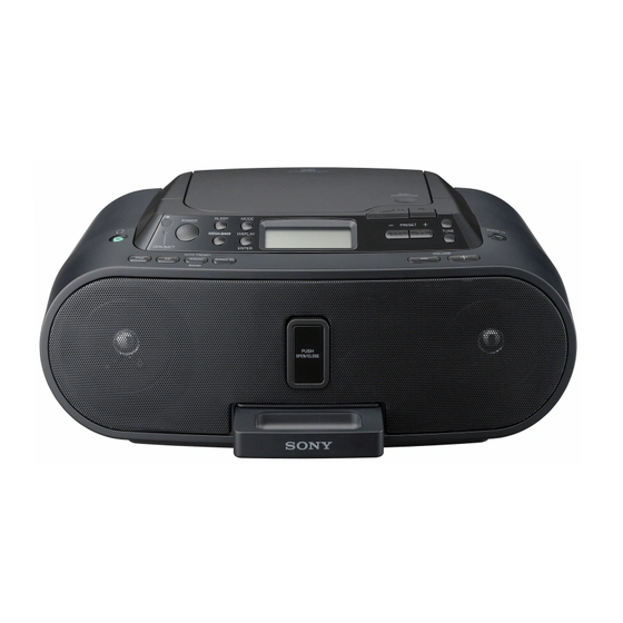
ZS-S2iP
Model Name Using Similar Mechanism CFD-S01
CD
CD Mechanism Type
Section
Optical Pick-up Name
SPECIFICATIONS
iPod section
DC out: 5 V
MAX: 500 mA
(AC only)
Compatible iPod models
The compatible iPod models are as follows. Update
your iPod to use the latest software before you use it.
iPod nano 2nd
generation
(aluminium)
iPod 4th generation
(color display)
PERSONAL AUDIO SYSTEM
US Model
Canadian Model
KSM-213CDP
KSS-213C
iPod nano 1st
iPod 5th
generation
generation (video)
iPod mini
iPod 4th
generation
– Continued on next page –
Advertisement
Table of Contents

Related Manuals for Sony ZSS2IPW


Summary of Contents for Sony ZSS2IPW
- Page 1 DC out: 5 V With 4-ohm loads, both channels driven from 150 -10,000 Hz; rated MAX: 500 mA 1 W per channel-minimum RMS power, with no more than 10 % total (AC only) harmonic distortion in AC operation. Compatible iPod models Other specifications The compatible iPod models are as follows.
- Page 2 AUDIO IN jack (stereo minijack) Power output The AC leakage from any exposed metal part to earth ground and 1.7 W + 1.7 W (at 4 Ω, 10% harmonic distortion) from all exposed metal parts to any exposed metal part having a Power requirements return to chassis, must not exceed 0.5 mA (500 microampers.).
- Page 3 NOTES ON LASER DIODE EMISSION CHECK The laser beam on this model is concentrated so as to be focused on the disc reflective surface by the objective lens in the optical pick- up block. Therefore, when checking the laser diode emission, observe from more than 30 cm away from the objective lens.
-
Page 4: Table Of Contents
5-2. Block Diagram – Main Section – ........20 5-3. Circuit Boards Location ..........21 5-4. Printed Wiring Board – Main Section (1/2) – ....22 5-5. Printed Wiring Boards – Main Section (2/2) – ....23 5-6. Schematic Diagram – Main Section (1/4) – ....24 5-7. -
Page 5: Servicing Notes
LASER DIODE AND FOCUS SEARCH OPERATION CHUCK PLATE JIG ON REPAIRING CHECK On repairing CD section, playing a disc without the lid (CD), use 1. Turn ON the [POWER] button and press [CD] button to CD Chuck Plate Jig. position. -
Page 6: General
Press the PUSH OPEN/CLOSE button Push the Sliding Tray into the unit. Notes • Do not carry the unit with an iPod set on the connector. Doing so may cause a malfunction. • Be sure to store the Sliding Tray before moving the unit. -
Page 7: Playing A Cd
• If you hear noise from the AM/FM while supplying power to iPod (“DC OUT” indicator appears in the display), press and hold MODE for a few seconds to stop the power supply to the iPod (“DC OUT” indicator disappears from the display). -
Page 8: Disassembly
ZS-S2iP SECTION 3 DISASSEMBLY Note: This set can be disassemble according to the following sequence. 3-1. CABINET (REAR) ASSY (Page 9) 3-2. CABINET (FRONT) ASSY, 3-11. POWER BOARD CABINET (UPPER) ASSY (Page 14) (Page 9) 3-3. MAIN BOARD 3-8. DOCK BLOCK ASSY 3-10. -
Page 9: Cabinet (Rear) Assy
ZS-S2iP Note: Follow the disassembly procedure in the numerical order given. 3-1. CABINET (REAR) ASSY 4 screw (+BV tapping (B2.6)) 1 battery case lid 5 two screws (+BV tapping (B2.6)) telescopic antenna 3 screw 7 CN305 (5P) (+BV tapping (B2.6)) -
Page 10: Main Board
3-3. MAIN BOARD cabinet (upper) assy qd CN906 (3P) 1 CN306 (4P) qs connector 2 CN311 (4P) (S801) qa flexible flat cable (6 core) 4 flexible flat cable (15 core) (CN702) (CN802) 0 flexible flat cable (16 core) (CN701) qf MAIN board... -
Page 11: Cd Motor Board, Optical Pick-Up
ZS-S2iP 3-5. CD MOTOR BOARD, OPTICAL PICK-UP 4 optical pick-up 3 CD MOTOR board 2 Remove the two solders. 1 Remove the two solders. 3-6. CONTROL BOARD 3 CONTROL board 2 three screws (+P tapping (B2.6)) 1 four screws (+P tapping (B2.6)) -
Page 12: Cd Lid
ZS-S2iP 3-7. CD LID 5 CD lid 6 CD spring cabinet (upper) assy 3-8. DOCK BLOCK ASSY 3 dock block assy 1 two screws (+BV tapping (B2.6)) 2 two screws (+BV tapping (B2.6)) cabinet (front) assy... -
Page 13: Dock Board
(+BTP 2 × 4) 3 three screws 6 two screws (+BTP 2 × 4) (+BTP 2 × 4) 3-10. KEY (FUNC) BOARD, KEY (VOL) BOARD 6 three screws 8 button (FUNC) (+BV tapping (B2.6)) 9 KEY (FUNC) board 7 two RETAINER boards 2 two screws (+BV tapping (B2.6)) -
Page 14: Power Board
ZS-S2iP 3-11. POWER BOARD 4 two screws (+BV tapping (B2.6)) 1 CN902 (2P) 5 POWER board 3 two screws (+BV tapping (B2.6)) 2 screw (+BV tapping (B2.6)) -
Page 15: Electrical Adjustments
(J321) • Connecting Digital Voltmeter (FM, AM) digital voltmeter 100 k Ω TP (VT) • Repeat the procedures in each adjustment several times, and the frequency coverage and tracking adjustments should be finally done by the trimmer capacitors. - Page 16 Adjustment Location: L3: AM FREQUENCY COVERAGE ADJUSTMENT CT1: FM TRACKING ADJUSTMENT L2: FM FREQUENCY COVERAGE ADJUSTMENT – MAIN BOARD (Component Side) – ANT1: AM TRACKING ADJUSTMENT CN701 CN702 CT3: AM TRACKING ADJUSTMENT L6: FM IF ADJUSTMENT L1: FM TRACKING ADJUSTMENT...
-
Page 17: Cd Section
CD section adjustments are done automatically in this set. In case of operation check, confirm that focus bias. Test Point: FOCUS BIAS CHECK 1. Connect the oscilloscope between IC701 pin ts and pin 4 (or – MAIN BOARD (Conductor Side) – TP (RF) and TP (VREF)). C707 2. - Page 18 ZS-S2iP MEMO...
-
Page 19: Diagrams
ZS-S2iP SECTION 5 DIAGRAMS 5-1. BLOCK DIAGRAM — CD SECTION — LDACO (O) CD_IN_ L DIGITAL MAIN AC (I) SYNCHRONOUS FILTER SECTION CIRCUIT & (Page 20) CD_IN_R 1-bit DAC BD (I) PRI- SERVO RF AMP, E (I) SYSTEM SERVO PROCESSOR,... -
Page 20: Block Diagram - Main Section
ZS-S2iP 5-2. BLOCK DIAGRAM — MAIN SECTION — ELECTRONIC VOLUME IC302 CD_IN_L IN L3 R–CH IN R3 SECTION CD_IN_R R–CH (Page 19) POWER AMP IC303 R-CH J321 J322 L OUT R–CH AUDIO IN R OUT 26 R–CH IN L2 IN R2 R–CH... -
Page 21: Circuit Boards Location
For printed wiring boards. REG board Note: Note: • All capacitors are in µF unless otherwise noted. (p: pF) • X : parts extracted from the component side. • Y : parts extracted from the conductor side. BATTERY (1) board... -
Page 22: Printed Wiring Board - Main Section (1/2)
ZS-S2iP 5-4. PRINTED WIRING BOARD — MAIN SECTION (1/2) — • Refer to page 21 for Circuit Boards Location. : Uses unleaded solder. (Page 32) (Page 32) ANT2 POWER BOARD CN901 REG BOARD CN905 FM TELESCOPE ANTENNA MAIN BOARD (Page 23) -
Page 23: Printed Wiring Boards - Main Section (2/2)
ZS-S2iP 5-5. PRINTED WIRING BOARDS — MAIN SECTION (2/2) — • Refer to page 21 for Circuit Boards Location. : Uses unleaded solder. J321 J322 AUDIO IN CD MOTOR BOARD AUDIO IN BOARD M702 (SLED) HP BOARD FB102 (Page 22) -
Page 24: Schematic Diagram - Main Section (1/4)
ZS-S2iP • Refer to page 21 for Waveforms. 5-6. SCHEMATIC DIAGRAM — MAIN SECTION (1/4) — • Refer to page 34 for IC Block Diagrams. CN804 C971 C974 (Page 33) C970 R859 (Page 26) R897 C273 C271 R274 R271 C274... -
Page 25: Schematic Diagram - Main Section (2/4)
ZS-S2iP • Refer to page 21 for Waveforms. • Refer to page 34 for IC Block Diagrams. 5-7. SCHEMATIC DIAGRAM — MAIN SECTION (2/4) — • Refer to page 36 for IC Pin Description of IC701. R746 Q703 R742 R739... -
Page 26: Schematic Diagram - Main Section (3/4)
ZS-S2iP • Refer to page 21 for Waveforms. • Refer to page 34 for IC Block Diagrams. 5-8. SCHEMATIC DIAGRAM — MAIN SECTION (3/4) — • Refer to page 38 for IC Pin Description of IC801. CN801 R844 R847 R846... -
Page 27: Schematic Diagram - Main Section (4/4)
ZS-S2iP 5-9. SCHEMATIC DIAGRAM — MAIN SECTION (4/4) — • Refer to page 35 for IC Block Diagrams. CN301 CN302 TP161 FB102 TP102 FB101 FB301 J322 C164 FB202 TP202 FB201 TP261 C264 FB302 D325 D326 JC302 JC301 R258 R261 R161 R158... -
Page 28: Printed Wiring Board - Dock Section
ZS-S2iP 5-10. PRINTED WIRING BOARD — DOCK SECTION — • Refer to page 21 for Circuit Boards Location. : Uses unleaded solder. DOCK BOARD (SIDE A) DOCK BOARD (SIDE B) C1009 C1008 L1001 R1021 MAIN R1026 BOARD R1014 CN805 (Page 22) -
Page 29: Schematic Diagram - Dock Section
ZS-S2iP 5-11. SCHEMATIC DIAGRAM — DOCK SECTION — CN810 TP1009 FB1001 R1021 TP1010 TP1011 FB1002 R1026 TP1012 TP1013 FB1003 TP1014 TP1015 TP1016 CN811 R1016 TP1017 TP1001 TP1018 C1009 C1008 TP1019 TP1002 R1013 R1019 L1001 TP1003 TP1020 TP1021 R1014 TP1004 TP1022... -
Page 30: Printed Wiring Boards - Control Section
ZS-S2iP 5-12. PRINTED WIRING BOARDS — CONTROL SECTION — • Refer to page 21 for Circuit Boards Location. : Uses unleaded solder. CONTROL BOARD (Page 22) (Page 22) MAIN BOARD MAIN BOARD CN801 CN802 IC401 S403 CN402 R439 S410 S404... -
Page 31: Schematic Diagram - Control Section
ZS-S2iP 5-13. SCHEMATIC DIAGRAM — CONTROL SECTION — CN404 CN402 R426 R428 R429 R430 R406 R403 R404 R409 R410 R422 R432 R437 S401 S410 S411 S412 S404 S403 R435 R419 R418 R424 R413 CN401 CN403 TP401 S418 S416 S415 S402... -
Page 32: Printed Wiring Boards - Power Supply Section
ZS-S2iP 5-14. PRINTED WIRING BOARDS — POWER SUPPLY SECTION — • Refer to page 21 for Circuit Boards Location. : Uses unleaded solder. POWER BOARD BATTERY TERMINAL (1) BOARD T901 FH901 F902 FH902 C901 D901 MAIN BOARD D904 C903 CN305... -
Page 33: Schematic Diagram - Power Supply Section
ZS-S2iP 5-15. SCHEMATIC DIAGRAM — POWER SUPPLY SECTION — CN902 CN903 J901 T901 F902 FH901 FH902 CN901 R910 R908 C915 (Page 27) IC901 Q901 CN905 JW908 C905 R905 C918 R906 R907 D909 (Page 27) R912 R917 CN906 Q902 C912 C913... - Page 34 ZS-S2iP • IC BLOCK DIAGRAMS IC1 LV23003VA (MAIN Board (1/4)) IC703 BA5826FP-E2 (MAIN Board (2/4)) SP– D.BUFF AM RF-IN 36 FM RF-IN 35 GND2 D.BUFF D.BUFF LEVEL 34 FM RF-OUT SL– SHIFT 33 VCC2 D.BUFF SPIN LEVEL FM MIX-OUT 32 FM OSC...
- Page 35 ZS-S2iP IC302 R2S15904SP (MAIN Board (4/4)) IN-R4 IN-R3 INPUT IN-R2 SELECTOR L-OUT IN-R1 MUTE R-OUT IN-L1 A-GND MODE SELECTOR IN-L2 INPUT SELECTOR IN-L3 REF-IN IN-L4 INPUT GAIN CONTROL MUTE IGOUT-L DATA 0 - +12dB /2dB step VOLUME VOLIN-L 0 - -89dB.
- Page 36 ZS-S2iP • IC PIN DESCRIPTIONS • IC701 BU9532KS2 (RF AMP, SYSTEM SERVO PROCESSOR, DIGITAL SIGNAL PROCESSOR) (MAIN BOARD (2/4)) Pin No. Pin Name Pin Description AVDD1 Power supply pin (+3.3 V) AC (I) A+C RF signal input BD (I) B+D RF signal input...
- Page 37 ZS-S2iP Pin No. Pin Name Pin Description TEN (O) Tracking error input CACG (O) RFAGC time constant capacitor fitted RFI (I) RF capacitor fitted EQO (O) RF EQ output...
- Page 38 Power supply 5 V voltage detect check signal input 6V-CHK Power supply 6 V voltage detect check signal input 3V-CHK Power supply CD 3.3 V voltage detect check signal input 43 to 45 KEY3 to 1 Key signal input AC IN...
- Page 39 Pin Description Main system oscillation signal output (4.915 MHz) System reset signal input V-CLK Serial transfer clock signal output to electronic volume V-DATA Serial transfer data signal output to electronic volume Serial transfer clock signal output to EEPROM Serial transfer data signal input/output to EEPROM...
-
Page 40: Exploded Views
Some delay should be anticipated Parts Color Cabinet’s Color specified. when ordering these items. • Accessories are given in the last of this parts list. • -XX and -X mean standardized parts, so • Abbreviation Les composants identifiés par une... -
Page 41: Front Cabinet Section
3-268-447-11 PLATE (OPEN), ORNAMENTAL (for BLACK) 3-268-445-11 BUTTON (VOL) (for BLACK) 3-268-463-01 SPRING (BUTTON OPEN) 1-831-616-21 CABLE, FLEXIBLE FLAT (4 CORE) X-2186-638-1 CABINET (FRONT) SUB ASSY (for WHITE) (US) 3-831-441-99 SHEET (1) SP101 1-826-280-51 SPEAKER (7.7cm) (L-CH) X-2186-643-1 CABINET (FRONT) SUB ASSY (for BLACK) (US) SP201 1-826-280-51 SPEAKER (7.7cm) (R-CH) -
Page 42: Dock Block Assy
4-951-620-01 SCREW (2.6X8), +BVTP 3-268-450-01 HOLDER (SPRING CLICK) 3-268-451-01 COVER (HOLDER DOCK) 3-268-464-01 SPRING (DOCK OPEN) X-2186-640-1 CASE (DOCK UPPER) SUB ASSY (for WHITE) 3-268-460-01 PLATE (HOLDER DOCK) X-2186-645-1 CASE (DOCK UPPER) SUB ASSY (for BLACK) 3-268-452-01 COVER (SPRING OPEN) -
Page 43: Upper Cabinet Section (1)
3-252-827-01 SCREW (B2.6), (+) BV TAPPING 3-019-395-01 PLATE, CHUCKING A-1336-418-A MAIN BOARD, COMPLETE 3-253-143-01 SCREW (B2.6), (+) P TAPPING 2-666-526-01 PAPER (B), SHIELD 2-654-056-31 HANDLE (for WHITE) 3-923-151-01 CUSHION, RUBBER 2-654-056-41 HANDLE (for BLACK) S801 1-692-960-11 SWITCH, PUSH (1 KEY) (Z OPEN/CLOSE) -
Page 44: Upper Cabinet Section (2)
4-951-620-01 SCREW (2.6X8), +BVTP 3-255-102-01 WASHER, PETP A-1336-415-A REG BOARD, COMPLETE 3-831-441-11 CUSHION (D) 3-274-789-01 HOLDER (REG) X-2186-639-1 CABINET (UPPER) SUB ASSY (for WHITE) 3-252-827-01 SCREW (B2.6), (+) BV TAPPING X-2186-644-1 CABINET (UPPER) SUB ASSY (for BLACK) 2-654-055-11 CHASSIS, CD IC401 6-600-108-01 IC RPM7140 (IR) 3-253-143-01 SCREW (B2.6), (+) P TAPPING... -
Page 45: Electrical Parts List
: µA.. uPA.. : µPA.. Les composants identifiés par une marque 0 sont critiques pour • RESISTORS uPB.. : µPB.. uPC.. : µPC.. uPD.. : µPD.. All resistors are in ohms. • CAPACITORS la sécurité. METAL:Metal-film resistor. uF : µF Ne les remplacer que par une piéce... - Page 46 1/10W C116 1-162-927-11 CERAMIC CHIP 100PF < SWITCH > C216 1-162-927-11 CERAMIC CHIP 100PF S401 1-786-050-21 SWITCH, KEYBOARD (TUNE –) < CONNECTOR > S403 1-786-050-21 SWITCH, KEYBOARD (x) S404 1-786-050-21 SWITCH, KEYBOARD (u) CN308 1-815-445-11 PIN, CONNECTOR (PWB) 4P S407...
- Page 47 0.22uF C112 1-126-925-11 ELECT 470uF ********************* C115 1-126-960-11 ELECT 2-666-526-01 PAPER (B), SHIELD C119 1-104-658-11 ELECT 100uF 7-685-871-01 SCREW +BVTT 3X6 (S) C125 1-126-959-11 ELECT 0.47uF < ANTENNA > C127 1-125-891-11 CERAMIC CHIP 0.47uF C129 1-165-176-11 CERAMIC CHIP 0.047uF ANT1...
- Page 48 MAIN Ref. No. Part No. Description Remark Ref. No. Part No. Description Remark C326 1-126-934-11 ELECT 220uF C758 1-162-923-11 CERAMIC CHIP 47PF C327 1-162-923-11 CERAMIC CHIP 47PF C759 1-104-658-11 ELECT 100uF C330 1-107-826-11 CERAMIC CHIP 0.1uF C760 1-107-826-11 CERAMIC CHIP 0.1uF...
- Page 49 6-704-118-01 IC S-80828CNMC-B8NT2G < CONNECTOR > IC805 6-703-740-01 IC S-24CS02AFT-TB-G IC806 8-759-909-71 IC BA4558F CN301 1-815-551-11 PIN, CONNECTOR (PWB) 3P CN305 1-815-553-11 PIN, CONNECTOR (PWB) 5P < JUMPER RESISTOR > CN306 1-815-552-11 PIN, CONNECTOR (PWB) 4P * CN311 1-815-552-21 PIN, CONNECTOR (PWB) 4P...
- Page 50 ZS-S2iP MAIN Ref. No. Part No. Description Remark Ref. No. Part No. Description Remark 1-216-829-11 METAL CHIP 4.7K 1/10W R175 1-216-833-11 METAL CHIP 1/10W 1-216-797-11 METAL CHIP 1/10W R178 1-216-864-11 SHORT CHIP 1-216-833-11 METAL CHIP 1/10W R234 1-216-813-11 METAL CHIP...
- Page 51 ZS-S2iP MAIN Ref. No. Part No. Description Remark Ref. No. Part No. Description Remark R712 1-216-837-11 METAL CHIP 1/10W R783 1-216-825-11 METAL CHIP 2.2K 1/10W R713 1-216-833-11 METAL CHIP 1/10W R784 1-216-813-11 METAL CHIP 1/10W R714 1-216-833-11 METAL CHIP 1/10W...
- Page 52 1-216-841-11 METAL CHIP 1/10W < CONNECTOR > R895 1-216-813-11 METAL CHIP 1/10W R896 1-216-813-11 METAL CHIP 1/10W CN902 1-815-443-11 PIN, CONNECTOR (PWB) 2P R897 1-216-821-11 METAL CHIP 1/10W R898 1-216-809-11 METAL CHIP 1/10W < DIODE > R899 1-216-825-11 METAL CHIP 2.2K...
- Page 53 1-831-623-21 CABLE, FLEXIBLE FLAT (16 CORE) 0 205 8-820-126-02 OPTICAL PICK-UP (KSM-213CDP/C2NP) ANT2 1-754-376-11 ANTENNA, TELESCOPIC (FM) 0 F902 1-533-469-12 FUSE, GLASS TUBE (DIA. 5) (2.5A/250V) IC901 6-711-961-01 IC NJM2388F05 0 J901 1-540-009-12 INLET, AC (- AC IN) S801 1-692-960-11 SWITCH, PUSH (1 KEY) (Z OPEN/CLOSE) SP101 1-826-280-51 SPEAKER (7.7cm) (L-CH)
- Page 54 ZS-S2iP REVISION HISTORY Clicking the version allows you to jump to the revised page. Also, clicking the version at the upper on the revised page allows you to jump to the next revised page. Ver. Date Description of Revision 2007. 08...