
Related Manuals for Alinco DJ-175


Summary of Contents for Alinco DJ-175
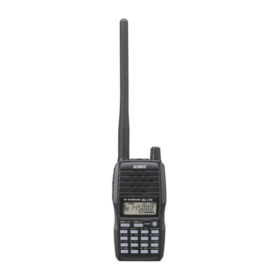
- Page 1 Service Manual DJ-175 Specifications Circuit Description Parts List Exploded View PC Board View Adjustment Schematic Diagram Block Diagram ALINCO, INC.
- Page 2 SPECIFICATIONS DJ-175 <GRNERAL> Frequency range: TX 144 ~ 147.995MHz *144 ~ 147.995MHz RX 136 ~ 173.995MHz *144 ~ 147.995MHz TX 144 ~ 145.995MHz *144 ~ 145.995MHz RX 144 ~ 145.995MHz *144 ~ 145.995MHz TFH: TX 136 ~ 173.995MHz *150 ~ 173.995MHz RX 136 ~ 173.995MHz...
-
Page 3: Circuit Description
CIRCUIT DESCRIPTION 1) Receiver System The receiver system is a double superheterodyne system with a 21.7MHz first IF and a 450kHz second IF. 1.Front End The received signal at frequency in the 136~173.995MHz (E version: 144~145.995MHz) range is passed through the low-pass filter (L101, L102, L104, L118, C101, 108, C109, C110, C117, C118, C119, C123, C124, C125, C126, C127, and C188) and tuning circuit (C255, C256, C257, C258, D120, L138, and L139) and amplified by the RF amplifier (Q119). -
Page 4: Transmitter System
4. Audio Circuit The audio signal from pin 9 of IC103 is amplified by the AF amplifier (Q120). The signal is then input to pin 16 of the electronic volume (IC105) for volume adjustment, and output from pin 14. The adjusted signal is sent to the audio power amplifier (IC104) through pin 2 to drive the speaker. - Page 5 3) PLL Synthesizer System 1. PLL The dividing ratio is obtained by sending data from the CPU (IC113) to pin 10 and sending clock pulse to pin 9 of the PLL IC ( IC101 ). The oscillated signal from the VCO is amplified by the buffer (Q116) and input to pin 8 of IC102. Each programmable divider in IC102 divides the frequency of the input signal by N according to the frequency data, to generate a comparison frequency of 5 or 6.25kHz.
-
Page 6: Cpu And Peripheral Circuits
4) CPU and Peripheral Circuits 1. LCD Display Circuit The CPU turns ON the LCD via segment and common terminals with 1/4 the duty and 1/3 the bias, at the frame frequency is 112.5Hz. 2. Display Lamp Circuit When the LAMP key is pressed, “L” is output form pin 67 of CPU ( IC113) to the bases of Q140. - Page 7 8. CTCSS, DCS Decoder The voice band of the AF output signal from pin 9 of IC103 is cut by sharp active filter IC111 and amplified, then led to pin 80 of CPU. The input signal is compared with the programmed tone frequency code in the CPU. The squelch will open when they match.
-
Page 8: Parts List
Parts List MAIN UNIT Ref. No. Parts No. Parts name Version Ref. No. Parts No. Parts name C101 CU3535 GRM36B102K50PT C173 C102 CU3535 GRM36B102K50PT C174 C103 CU3519 GRM36CH470J50PT C175 C104 CU3535 GRM36B102K50PT C176 CU3502 GRM36CK010C50PT C105 C177 CU3535 GRM36B102K50PT C108 CU3535 GRM36B102K50PT C178... - Page 9 Ref. No. Parts No. Parts name Version Ref. No. Parts No. Parts name C239 CU3547 GRM36B103K16PT C305 CU3138 GRM188B31C225KE14D T, E, EUK C240 CU3535 GRM36B102K50PT C306 CU3559 GRM155B30J105KE18D C241 CU3539 GRM36B222K50PT C307 CU3535 GRM36B102K50PT C242 CU3535 GRM36B102K50PT C308 CU3138 GRM188B31C225KE14D C243 CU3573 GRM1554C1HR80BZ01D...
- Page 10 Ref. No. Parts No. Parts name Version Ref. No. Parts No. Parts name C371 CU3535 GRM36B102K50PT D130 XD0418 RB521S-30TE61 C372 CU3559 GRM155B30J105KE18D FL101 XF0059 Q21707AD27-21.7MHZ C373 FL101 XF0051 Q2175AD20 21.7MHZ T, E, TFH C375 CU3541 GRM36B332K50PT FL102 XF0059 Q21707AD27-21.7MHZ C376 CU3554 GRM36B104K10PT FL102...
- Page 11 Ref. No. Parts No. Parts name Version Ref. No. Parts No. Parts name Q104 XT0210 2SC6026MFV-GR R136 RK3562 1005 1/16W 100K OHMJ Q105 XE0091 RQA0002DNS R137 RK3551 1005 1/16W 12K OHM J Q106 XE0092 RQA0004PXDQS R138 Q107 R141 Q108 XT0219 15GN03F-TL-E R142 RK3530...
- Page 12 Ref. No. Parts No. Parts name Version Ref. No. Parts No. Parts name R206 RK3536 1005 1/16W 680 OHM J R276 RK3552 1005 1/16W 15K OHM J R206 RK3539 1005 1/16W 1.2K OHMJ T, E, TFH R277 RK3552 1005 1/16W 15K OHM J R207 RK3536 1005 1/16W 680 OHM J...
- Page 13 Ref. No. Parts No. Parts name Version Ref. No. Parts No. Parts name R344 RK3537 1005 1/16W 820 OHM J KZ0219 FRONT CASE ASSYDJ175 R345 RK3546 1005 1/16W 4.7K OHMJ NK0081 KNOB R346 RK3562 1005 1/16W 100K OHMJ SD0111A BATTERY TERMINAL R347 RK3562 1005 1/16W 100K OHMJ...
- Page 14 NK0081 FG0480 FG0479 ES0027 FG0392 KZ0219 YX0045 DP0195 FG0478 AX0009...
- Page 15 ST0089 FP0324 EL0059 DG0046 FG0418 TL0033 AF0030 FG0234Y AF0003 AF0003 FM0300 UE0571 UR0027 AN0042 AN0034 SS0112 AF0003 FP0310 SD0137 FP0321 AF0003 SD0111A...
-
Page 16: Pc Board View
PC Board View MAIN - Side A... - Page 17 PC Board View MAIN - Side B...
- Page 18 PC Board View EDC165 Side-A T103 T101 T102 R102 R103 Side-B JK101 R101 D101 (Anode)
-
Page 19: Digital Multimeter
Adjustments: 1) Required Test Equipment The following items are required to adjust radio parameters 1.Regulated power supply Supply voltage: 7-8 DC Current: 3A or more 2.Digital multimeter Voltage range: FS = Approx. 20V Current: 10A or more Input resistance: High impedance 3.Oscilloscope Measurable frequency: Audio frequency... - Page 20 11.Linear detector Measurable frequency: Up to 200MHz Characteristics: Flat 60dB or more 12. DC Ammeter Current: 3A or more Note: (1). SSG initial setting Modulation Frequency:1kHz Modulation Level:3.0kHz (T, E, TFH)/ 1.5kHz (EUK) (2). Reference sensitivity: 12dB SINAD (3). Specified audio output level: 500mW at 8Ω (4).
-
Page 21: Adjustment Mode
2) Adjustment mode The adjustment should be operated in the Adjustment mode. Therefore except for the reference frequency, deviation and tone-deviation adjustments an operator won’t touch the components on the board, but most of the adjustments should be done by operating the dial and keys on the unit. During such operation, memory channels are used temporary therefore it is required to program memories before the unit is set to the adjustment mod. - Page 22 1. Frequency adjustment Select memory ch.1. Press PTT on the unit to transmit and measure the TX frequency. One of digits 00-FF should appear on the display where memory channel number was shown. Rotate the dial on the unit to adjust the frequency to bring the value to the range specified below. Specification value :±50Hz Necessary instrument: (1).
- Page 23 5. Microphone deviation Select memory ch.5. Input the signal as specified below from an Audio generator and transmit. Measure the deviation value using a Liner-detector. Press PTT on the unit to transmit. One of digits 00-FF should appear on the display where memory channel number was shown. Rotate the dial on the unit to adjust the deviation to meet the specification.
- Page 24 8. Receiver sensitivity adjustment Preparation: Set the speaker audio output level to 50mW. Operation: There are three points to be adjusted, the lower, central, and upper edges of the receiver’s covering range. Set the memory channels accordingly. Input an RF signal from the SSG to the antenna connector then measure output signal at the speaker jack using a SINAD meter.
- Page 25 9. Squelch adjustments: Select the memory channel number accordingly to adjust the level Min and Max. Input an RF signal to the antenna connector from SSG then press FUNC key on the unit. A beep (“pip” ) sounds and completes the adjustment. a.
- Page 26 1.2k 1.2k MACLH2GG TC75S56FU RN2107MFV 2.2/16V 100k 100k uPD78F0395GC 21.7M-W 1.2k 1.2k 150k 100k 100k uPD78F0395GC ALFYM450F MACLH2GG TC75S56FU RN2107MFV 2.2/16V 21.7M-W 1.2k 1.2k uPD78F0394GC ALFYM450F 21.7M-N 5.6k 150k 100k 100k uPD78F0395GC ALFYM450G TC75S56FU RN2107MFV 2.2/16V Schematic diagram DJ-175 CN102...
- Page 27 R101 56/3W T101 JK101 R102 D101 MVR3338S R103 T102 Schematic Diagram EDC-165...
- Page 28 5V REGULATOR IC106 SW-TX XC6202P502M BACK LIGHT Q136 LAMP SW 2SA1955FV D123 SML310MT D124 SML310MT Q133 RN1111MFV BATTERY 7.2V D125 SML310MT Q138 RN1111MFV D126 SML310MT Q140 RN1111MFV Q132 D128 SML310MT 2SC6026MFV D129 SML310MT RECEIVE TRANSMIT RECEIVE/TRANSMIT Block Diagram DJ-175 CPU CONTROL...