
Related Manuals for Toshiba RD-XS34SB


Summary of Contents for Toshiba RD-XS34SB
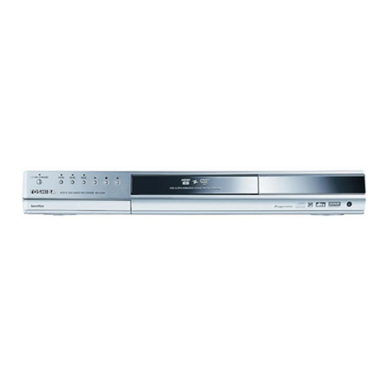
- Page 1 FILE NO. 810-200512 SERVICE MANUAL DIGITAL VIDEO HDD/DVD VIDEO RECORDER RD-XS34SB RD-XS34SF RD-XS34SG Feb., 2005...
- Page 2 LASER BEAM CAUTION LABEL When the power supply is being turned on, you may not remove this laser cautions label. If it removes, radiation of a laser may be received. PREPARATION OF SERVICING Pickup Head consists of a laser diode that is very susceptible to external static electricity. Although it operates properly after replacement, if it was subject to electrostatic discharge during replacement, its life might be shortened.
-
Page 3: Table Of Contents
CONTENTS SECTION 1 GENERAL DESCRIPTIONS 2. LOCATION OF MAIN PARTS 1. OPERATING INSTRUCTIONS 2-1. Location of Main Parts 2-2. Location of PC Boards SECTION 2 PART REPLACEMENT AND ADJUSTMENT PROCEDURES 1-2. PC Board Replacement 1. REPLACEMENT OF MECHANICAL PARTS 1-2-1. Tuner Unit PC Board 1-1. -
Page 4: Operating Instructions
SECTION 1 GENERAL DESCRIPTIONS 1. OPERATING INSTRUCTIONS Please refer to the owner's manual about the contents. - Page 5 2. LOCATION OF MAIN PARTS 2-1. Location of Main Parts RAM1 RAM DRIVE ZG45 FAN HDD1 HDD UNIT Fig. 1-2-1 2-2. Location of PC Boards EU82 Tuner Unit PC board EU05 Mother PC board EU01 Digital PC board EU55 Front (Jack) PC board EU02 Power PC board EU03B Front (L)
-
Page 6: Replacement Of Mechanical Parts
SECTION 2 PART REPLACEMENT AND ADJUSTMENT PROCEDURES CAUTIONS BEFORE STARTING PART REPLACEMENT Electronic parts are susceptible to static electricity and may easily damaged, so do not forget to ground as required. Many screws are used inside the unit. To prevent the screws from missing or dropping, etc. always use a magnetized screwdriver in servicing. -
Page 7: Hdd
1-1-2. HDD 1. Remove the top cover. (Refer to item 1-1-1.) 2. Peel off the tape (1). 3. Remove four screws (2). 4. Disconnect the flexible cable (3) and the connector (4). 5. Remove four screws (5) and four dampers (7), then remove the HDD (8). Note: •... -
Page 8: Front Panel
1-1-3. Front Panel 1. Remove the top cover. (Refer to item 1-1-1.) 2. Peel off three tapes (1). 3. Disconnect two connectors (2) and two flexible cables (3). 4. Remove two screws (4) and four claws, then remove the front panel (5). Note: •... -
Page 9: Ram Drive
1-1-4. RAM Drive 1. Remove the front panel. (Refer to item 1-1-3.) 2. Peel off three tapes (1). 3. Disconnect the flexible cable (2) and the connector (3). 4. Remove three screws (4), then remove the RAM drive (5). 5. Remove four screws (6), then remove the RAM drive bracket (7). Note: •... -
Page 10: Rear Panel
1-1-5. Rear Panel 1. Remove the top cover. (Refer to item 1-1-1.) 2. Peel off the tape (1). 3. Remove the screw (2), four screws (3) and five screws (4). 4. Remove two claws, then remove the rear panel (5). 5. -
Page 11: Pc Board Replacement
1-2. PC Board Replacement 1-2-1. Tuner Unit PC Board Tuner Unit PC board (3) 1. Remove the top cover. (Refer to item 1-1-1.) Screw (2) 2. Remove the screw (1) and the screw (2). 3. Remove the claw, then remove the Tuner Unit PC board (3). 4. - Page 12 1-2-3. Mother PC Board 1. Remove the Front panel. (Refer to item 1-1-3.) 2. Remove the Rear panel. (Refer to item 1-1-5.) 3. Remove the Tuner Unit PC board. (Refer to item 1-2-1.) 4. Remove the Digital PC board. (Refer to item 1-2-2.) 5.
- Page 13 1-2-4. Power PC Board Cautions : • Danger of explosion if battery is incorrectly replaced. • Replace only with the same or equivalent type. 1. Remove the top cover. (Refer to item 1-1-1.) 2. Disconnect three connectors (1) and the connector (2). 3.
-
Page 14: Front (R), Front (L) And Front (Jack) Pc Board
1-2-5. Front (R), Front (L) and Front (Jack) PC Boards 1. Remove the front panel. (Refer to item 1-1-3.) 2. Peel off two tapes (1). 3. Remove four screws (2), then remove the stay (3). 4. Remove four screws (4), then remove the Front (R) PC board (5). 5. -
Page 15: Tuner Unit Pc Board
2. WIRING CONNECTION DIAGRAM After the servicing is complete, return the wiring to its original state by using the diagram below as a reference. Tuner Unit PC board Mother PC board Power PC board W003 W056 W100 W051 Digital PC board W101 W055 W052... -
Page 16: Parts List
SECTION 4 PARTS LIST SAFETY PRECAUTION The parts identified by ! ( ) mark are critical for safety. Replace only with part number specified. The mounting position of replacement is to be identical with originals. The substitute replacement parts which do not have the same safety characteristics as specified in the parts list may create shock, fire or other hazards. -
Page 17: Exploded Views
ZF01 ZF35 (RD-XS34SF/SG) ZF23 ZF23 ZF23A (RD-XS34SB) Note: A clamp filter (ZF23A) is attached to a power cord (ZF23). Refer to the figure below for the installation. Power supply cable Turn the power supply cable 2 round in the clamp filter. -
Page 18: Chassis Assembly
1-2. Chassis Assembly ZG20A ZG20 EU82 W056 EU01 ZG45 W052 EU05 W051 EU02 W055 RAM1 W055A HDD1 W051A ZG50 EU55 EU03B EU03A ZG01 W053 Fig. 4-4-2... -
Page 19: Parts List
2. PARTS LIST *a: for RD-XS34SB, b: for RD-XS34SF, c: for RD-XS34SG Location Part No. Description - MECHANICAL PARTS - HDD1 P000428190 HDD,ST3160022ACECS 160GB ! RAM1 P000432490 DVD-RAM SW-9573-ETS W051 P000433820 Cable,Flexible FFC,40P,L280 W051A P000391300 CONV Unit,ATAPI-FFC W052 P000435000 Cable,Flexible... - Page 20 *a: for RD-XS34SB, b: for RD-XS34SF, c: for RD-XS34SG Location Part No. Description - ELECTRICAL PARTS - EU01 P000435040 PC Board Assy Digital,RD-XS34SB EU01 P000435100 PC Board Assy Digital,RD-XS34SF EU01 P000435120 PC Board Assy Digital,RD-XS34SG - INTEGRATED CIRCUITS - IC302...
- Page 21 *a: for RD-XS34SB, b: for RD-XS34SF, c: for RD-XS34SG Location Part No. Description Q104 79050089 Transistor RN2401 Q108 79050089 Transistor RN2401 Q109 79050089 Transistor RN2401 - DIODES - D103 79060077 Diode,LED SLA-360MT D104 P000416670 Diode,LED EL-3105-1VRT - MISCELLANEOUS - S100...
- Page 22 *a: for RD-XS34SB, b: for RD-XS34SF, c: for RD-XS34SG Location Part No. Description QB21 P000395120 Transistor,Chip 2SC2714-Y QW01 79050016 Transistor,Chip 2SC2712-Y QW02 79050043 Transistor,Chip RN1402 QW03 79050016 Transistor,Chip 2SC2712-Y QW04 79050016 Transistor,Chip 2SC2712-Y QW05 79050016 Transistor,Chip 2SC2712-Y QW06 79050001 Transistor,Chip...
- Page 23 *a: for RD-XS34SB, b: for RD-XS34SF, c: for RD-XS34SG Location Part No. Description JX03 P000434970 Connector,RGB MRC-021V-29PC K901 P000405010 Relay ATX209 K902 P000405010 Relay ATX209 K903 P000405010 Relay ATX209 X700 P000391040 Crystal X701 P000363400 Oscillator,Crystal X702 P000395090 Resonator,Ceramic FCR4.43MC5AT X703...
- Page 24 Specification Specification RD-XS34SB 1/2 ■ Power requirement during operation ■ VIDEO input 1.0Vp-p (75Ω), Sync signal negative, Pin jack x 1 system, 1 in front ■ Power requirement at standby SCART socket x 2 at rear 4.3W (Eco mode: off) ■...
- Page 25 RD-XS34SB 2/2 ■ DIGITAL AUDIO OUTPUT BITSTREAM/PCM (OPTICAL terminal) Optical connector x 1 system ■ DIGITAL AUDIO OUTPUT BITSTREAM/PCM (COAXIAL terminal) 0.5Vp-p (75Ω), pin jack x 1 system ■ CHANNEL CHANGE IR jack This is for connection of the supplied IR control cable only.
- Page 26 Specification Specification Specification RD-XS34SF 1/2 I Power requirement during operation I VIDEO input 1.0Vp-p (75Ω), Sync signal negative, Pin jack x 1 system, 1 in front I Power requirement at standby PERITEL socket x 2 at rear 4.3W (Eco mode: off) I VIDEO output 1.9W (Eco mode: on) 1.0Vp-p (75Ω), Sync signal negative,...
- Page 27 Specification RD-XS34SF 2/2 I DIGITAL AUDIO OUTPUT BITSTREAM/PCM (OPTICAL terminal) Optical connector x 1 system I DIGITAL AUDIO OUTPUT BITSTREAM/PCM (COAXIAL terminal) 0.5Vp-p (75Ω), pin jack x 1 system I CHANNEL CHANGE IR jack This is for connection of the supplied IR control cable only.
- Page 28 Specification Specification Specification RD-XS34SG 1/2 I Power requirement during operation I VIDEO input 1.0Vp-p (75Ω), Sync signal negative, Pin jack x 1 system, 1 in front I Power requirement at standby SCART socket x 2 at rear 4.3W (Eco mode: off) I VIDEO output 1.9W (Eco mode: on) 1.0Vp-p (75Ω), Sync signal negative,...
- Page 29 Specification RD-XS34SG 2/2 I DIGITAL AUDIO OUTPUT BITSTREAM/PCM (OPTICAL terminal) Optical connector x 1 system I DIGITAL AUDIO OUTPUT BITSTREAM/PCM (COAXIAL terminal) 0.5Vp-p (75Ω), pin jack x 1 system I CHANNEL CHANGE IR jack This is for connection of the supplied IR control cable only.
- Page 30 1 1, SHIBAURA 1 CHOME, MINATO KU, TOKYO 105 8001, JAPAN...
- Page 31 FILE NO. 810-200512 SERVICE MANUAL DIGITAL VIDEO HDD/DVD VIDEO RECORDER RD-XS34SB RD-XS34SF RD-XS34SG Feb., 2005...
- Page 32 LASER BEAM CAUTION LABEL When the power supply is being turned on, you may not remove this laser cautions label. If it removes, radiation of a laser may be received. PREPARATION OF SERVICING Pickup Head consists of a laser diode that is very susceptible to external static electricity. Although it operates properly after replacement, if it was subject to electrostatic discharge during replacement, its life might be shortened.
- Page 33 CONTENTS SECTION 1 GENERAL DESCRIPTIONS 2. LOCATION OF MAIN PARTS 1. OPERATING INSTRUCTIONS 2-1. Location of Main Parts 2-2. Location of PC Boards SECTION 2 PART REPLACEMENT AND ADJUSTMENT PROCEDURES 1-2. PC Board Replacement 1. REPLACEMENT OF MECHANICAL PARTS 1-2-1. Tuner Unit PC Board 1-1.
-
Page 34: Operating Instructions
SECTION 1 GENERAL DESCRIPTIONS 1. OPERATING INSTRUCTIONS Please refer to the owner's manual about the contents. - Page 35 2. LOCATION OF MAIN PARTS 2-1. Location of Main Parts RAM1 RAM DRIVE ZG45 FAN HDD1 HDD UNIT Fig. 1-2-1 2-2. Location of PC Boards EU82 Tuner Unit PC board EU05 Mother PC board EU01 Digital PC board EU55 Front (Jack) PC board EU02 Power PC board EU03B Front (L)
-
Page 36: Replacement Of Mechanical Parts
SECTION 2 PART REPLACEMENT AND ADJUSTMENT PROCEDURES CAUTIONS BEFORE STARTING PART REPLACEMENT Electronic parts are susceptible to static electricity and may easily damaged, so do not forget to ground as required. Many screws are used inside the unit. To prevent the screws from missing or dropping, etc. always use a magnetized screwdriver in servicing. -
Page 37: Hdd
1-1-2. HDD 1. Remove the top cover. (Refer to item 1-1-1.) 2. Peel off the tape (1). 3. Remove four screws (2). 4. Disconnect the flexible cable (3) and the connector (4). 5. Remove four screws (5) and four dampers (7), then remove the HDD (8). Note: •... -
Page 38: Front Panel
1-1-3. Front Panel 1. Remove the top cover. (Refer to item 1-1-1.) 2. Peel off three tapes (1). 3. Disconnect two connectors (2) and two flexible cables (3). 4. Remove two screws (4) and four claws, then remove the front panel (5). Note: •... -
Page 39: Ram Drive
1-1-4. RAM Drive 1. Remove the front panel. (Refer to item 1-1-3.) 2. Peel off three tapes (1). 3. Disconnect the flexible cable (2) and the connector (3). 4. Remove three screws (4), then remove the RAM drive (5). 5. Remove four screws (6), then remove the RAM drive bracket (7). Note: •... -
Page 40: Rear Panel
1-1-5. Rear Panel 1. Remove the top cover. (Refer to item 1-1-1.) 2. Peel off the tape (1). 3. Remove the screw (2), four screws (3) and five screws (4). 4. Remove two claws, then remove the rear panel (5). 5. -
Page 41: Pc Board Replacement
1-2. PC Board Replacement 1-2-1. Tuner Unit PC Board Tuner Unit PC board (3) 1. Remove the top cover. (Refer to item 1-1-1.) Screw (2) 2. Remove the screw (1) and the screw (2). 3. Remove the claw, then remove the Tuner Unit PC board (3). 4. - Page 42 1-2-3. Mother PC Board 1. Remove the Front panel. (Refer to item 1-1-3.) 2. Remove the Rear panel. (Refer to item 1-1-5.) 3. Remove the Tuner Unit PC board. (Refer to item 1-2-1.) 4. Remove the Digital PC board. (Refer to item 1-2-2.) 5.
-
Page 43: Power Pc Board
1-2-4. Power PC Board Cautions : • Danger of explosion if battery is incorrectly replaced. • Replace only with the same or equivalent type. 1. Remove the top cover. (Refer to item 1-1-1.) 2. Disconnect three connectors (1) and the connector (2). 3. -
Page 44: Front (R), Front (L) And Front (Jack) Pc Board
1-2-5. Front (R), Front (L) and Front (Jack) PC Boards 1. Remove the front panel. (Refer to item 1-1-3.) 2. Peel off two tapes (1). 3. Remove four screws (2), then remove the stay (3). 4. Remove four screws (4), then remove the Front (R) PC board (5). 5. -
Page 45: Tuner Unit Pc Board
2. WIRING CONNECTION DIAGRAM After the servicing is complete, return the wiring to its original state by using the diagram below as a reference. Tuner Unit PC board Mother PC board Power PC board W003 W056 W100 W051 Digital PC board W101 W055 W052... -
Page 46: Parts List
SECTION 4 PARTS LIST SAFETY PRECAUTION The parts identified by ! ( ) mark are critical for safety. Replace only with part number specified. The mounting position of replacement is to be identical with originals. The substitute replacement parts which do not have the same safety characteristics as specified in the parts list may create shock, fire or other hazards. -
Page 47: Exploded Views
ZF01 ZF35 (RD-XS34SF/SG) ZF23 ZF23 ZF23A (RD-XS34SB) Note: A clamp filter (ZF23A) is attached to a power cord (ZF23). Refer to the figure below for the installation. Power supply cable Turn the power supply cable 2 round in the clamp filter. -
Page 48: Chassis Assembly
1-2. Chassis Assembly ZG20A ZG20 EU82 W056 EU01 ZG45 W052 EU05 W051 EU02 W055 RAM1 W055A HDD1 W051A ZG50 EU55 EU03B EU03A ZG01 W053 Fig. 4-4-2... -
Page 49: Parts List
2. PARTS LIST *a: for RD-XS34SB, b: for RD-XS34SF, c: for RD-XS34SG Location Part No. Description - MECHANICAL PARTS - HDD1 P000428190 HDD,ST3160022ACECS 160GB ! RAM1 P000432490 DVD-RAM SW-9573-ETS W051 P000433820 Cable,Flexible FFC,40P,L280 W051A P000391300 CONV Unit,ATAPI-FFC W052 P000435000 Cable,Flexible... - Page 50 *a: for RD-XS34SB, b: for RD-XS34SF, c: for RD-XS34SG Location Part No. Description - ELECTRICAL PARTS - EU01 P000435040 PC Board Assy Digital,RD-XS34SB EU01 P000435100 PC Board Assy Digital,RD-XS34SF EU01 P000435120 PC Board Assy Digital,RD-XS34SG - INTEGRATED CIRCUITS - IC302...
- Page 51 *a: for RD-XS34SB, b: for RD-XS34SF, c: for RD-XS34SG Location Part No. Description Q104 79050089 Transistor RN2401 Q108 79050089 Transistor RN2401 Q109 79050089 Transistor RN2401 - DIODES - D103 79060077 Diode,LED SLA-360MT D104 P000416670 Diode,LED EL-3105-1VRT - MISCELLANEOUS - S100...
- Page 52 *a: for RD-XS34SB, b: for RD-XS34SF, c: for RD-XS34SG Location Part No. Description QB21 P000395120 Transistor,Chip 2SC2714-Y QW01 79050016 Transistor,Chip 2SC2712-Y QW02 79050043 Transistor,Chip RN1402 QW03 79050016 Transistor,Chip 2SC2712-Y QW04 79050016 Transistor,Chip 2SC2712-Y QW05 79050016 Transistor,Chip 2SC2712-Y QW06 79050001 Transistor,Chip...
- Page 53 *a: for RD-XS34SB, b: for RD-XS34SF, c: for RD-XS34SG Location Part No. Description JX03 P000434970 Connector,RGB MRC-021V-29PC K901 P000405010 Relay ATX209 K902 P000405010 Relay ATX209 K903 P000405010 Relay ATX209 X700 P000391040 Crystal X701 P000363400 Oscillator,Crystal X702 P000395090 Resonator,Ceramic FCR4.43MC5AT X703...
- Page 54 Specification Specification RD-XS34SB 1/2 ■ Power requirement during operation ■ VIDEO input 1.0Vp-p (75Ω), Sync signal negative, Pin jack x 1 system, 1 in front ■ Power requirement at standby SCART socket x 2 at rear 4.3W (Eco mode: off) ■...
- Page 55 RD-XS34SB 2/2 ■ DIGITAL AUDIO OUTPUT BITSTREAM/PCM (OPTICAL terminal) Optical connector x 1 system ■ DIGITAL AUDIO OUTPUT BITSTREAM/PCM (COAXIAL terminal) 0.5Vp-p (75Ω), pin jack x 1 system ■ CHANNEL CHANGE IR jack This is for connection of the supplied IR control cable only.
- Page 56 Specification Specification Specification RD-XS34SF 1/2 ■ Power requirement during operation ■ VIDEO input 1.0Vp-p (75Ω), Sync signal negative, Pin jack x 1 system, 1 in front ■ Power requirement at standby PERITEL socket x 2 at rear 4.3W (Eco mode: off) ■...
- Page 57 Specification RD-XS34SF 2/2 ■ DIGITAL AUDIO OUTPUT BITSTREAM/PCM (OPTICAL terminal) Optical connector x 1 system ■ DIGITAL AUDIO OUTPUT BITSTREAM/PCM (COAXIAL terminal) 0.5Vp-p (75Ω), pin jack x 1 system ■ CHANNEL CHANGE IR jack This is for connection of the supplied IR control cable only.
- Page 58 Specification Specification Specification RD-XS34SG 1/2 ■ Power requirement during operation ■ VIDEO input 1.0Vp-p (75Ω), Sync signal negative, Pin jack x 1 system, 1 in front ■ Power requirement at standby SCART socket x 2 at rear 4.3W (Eco mode: off) ■...
- Page 59 Specification RD-XS34SG 2/2 ■ DIGITAL AUDIO OUTPUT BITSTREAM/PCM (OPTICAL terminal) Optical connector x 1 system ■ DIGITAL AUDIO OUTPUT BITSTREAM/PCM (COAXIAL terminal) 0.5Vp-p (75Ω), pin jack x 1 system ■ CHANNEL CHANGE IR jack This is for connection of the supplied IR control cable only.
- Page 60 1 1, SHIBAURA 1 CHOME, MINATO KU, TOKYO 105 8001, JAPAN...
- Page 61 FILE NO. 810-200512 SERVICE MANUAL DIGITAL VIDEO HDD/DVD VIDEO RECORDER RD-XS34SB RD-XS34SF RD-XS34SG Feb., 2005...
- Page 62 SECTION 3 SERVICING DIAGRAMS 1. CIRCUIT SYMBOLS AND SUPPLEMENTARY EXPLANATION 1-1. Precautions for Part Replacement • In the schematic diagram, parts marked (ex. • Using the parts other than those specified shall violate the regulations, and may cause troubles such as F801) are critical part to meet the safety regulations, operation failures, fire etc.
- Page 63 1-4. Inductor Indication Eg. 4 ... H None Unit ... mH ... mH Tolerance None ... ±5% ... ±0.1% ... ±0.25% ... ±0.5% ... ±1% Type name ... ±2% ... ±10% ... ±20% Fig. 3-1-4 1-5. Waveform and Voltage Measurement Eg.
- Page 64 2. PRINTED WIRING BOARD AND SCHEMATIC DIAGRAM PARALLEL W102L W102J PARALLEL EVER 5V EVER 5V Eject_key Eject_key ON/OFF 5V ON/OFF 5V LED_OUT0 LED_OUT0 Door Sensor Door Sensor LED_OUT3 LED_OUT3 W101 LED_OUT_1 LED_OUT_1 EU55 EU03A W102 connector EU03B Power_key Power_key PowerLED PowerLED FRONT (JACK) FRONT (R)
- Page 65 3. BLOCK DIAGRAMS 3-1. Overall Block Diagram IC504 uPD72852AGB-8EU-A 24.576MHz Type: SD-W3002 1394 PHY DVD RAM/RW Drive IC502 IC503 Audio LPF uPD72893AGD-LML-A 16Mbit &Amplifier 80GB Hard DisK Drive OUT_1 12.288MHz SDRAM 1394 AV LINK ANALOG CIRCUI OPTICAL. DIGITAL.OUT IC512 CV-in 24.576MHz IC301 AV_1...
- Page 66 4. CIRCUIT DIAGRAMS 4-1. Power Supply Circuit Diagram Fig. 3-4-1...
- Page 67 4-2. Front Circuit Diagram 4-2-1. Front Jack Circuit Diagram Fig. 3-4-2...
- Page 68 4-2-2. Front Circuit Diagram (L/R) Fig. 3-4-3...
- Page 69 4-3. Digital Circuit Diagram 4-3-1. Digital 1 Circuit Diagram Fig. 3-4-4...
- Page 70 4-3. Digital Circuit Diagram 4-3-1. Digital 1 Circuit Diagram...
- Page 77 Fig. 3-4-4...
- Page 78 4-3-2. Digital 2 Circuit Diagram Fig. 3-4-5...
- Page 79 4-3-2. Digital 2 Circuit Diagram...
- Page 84 Fig. 3-4-5...
- Page 85 4-4. Mother Circuit Diagram 4-4-1. Tuner Interface Circuit Diagram Fig. 3-4-6...
- Page 86 4-4-2. Timer Circuit Diagram Fig. 3-4-7...
- Page 87 4-4-3. Audio Circuit Diagram TB=RDXS34SB TF=RDXS34SF TG=RDXS34SG Fig. 3-4-8...
- Page 88 4-4-4. Video Circuit Diagram DIFFERENCE PARTS (FOR RD-XS34SF/SG) Fig. 3-4-9...
- Page 89 4-4-5. MSP Circuit Diagram Fig. 3-4-10...
- Page 90 4-5. Tuner Unit Circuit Diagram Fig. 3-4-11...
- Page 91 5. PC BOARDS 5-1. Front Jack PC Board Fig. 3-5-1 EU55 Front Jack PC Broad (Top side) Fig. 3-5-2 EU55 Front Jack PC Broad (Bottom side) 5-2. Front (L) PC Board Fig. 3-5-3 EU03B Front (L) PC Broad (Top side) Fig.
- Page 92 5-3. Front (R) PC Board Fig. 3-5-5 EU03A Front (R) PC Broad (Top side) Fig. 3-5-6 EU03A Front (R) PC Broad (Bottom side)
- Page 93 5-4. Tuner Unit PC Board CB92 RB92 CB95 RB97 CB94 RB98 CB93 CB96 RB99 RB94 RB96 RB93 RB95 Fig. 3-5-7 EU82 Tuner Unit PC Broad (Top side) Fig. 3-5-8 EU82 Tuner Unit PC Broad (Bottom side)
- Page 94 5-5. Digital PC Board R350 C364 R335 R334 IC303 IC302 C352 R332 IC304 R330 R331 R333 R329 R344 R343 R342 R341 R340 R339 C347 C333 C353 X301 RM302 RM301 C302 C350 C324 E308 C320 TP787 TP842 R322 TP872 C319 C598 TP840 TP841 C323...
- Page 95 5-6. Mother PC Board Fig. 3-5-11 EU05 Mother PC Board (Top side)
- Page 96 Fig. 3-5-12 EU05 Mother PC Board (Bottom side)