Table of Contents
Advertisement
Quick Links
SERVICE MANUAL
This service manual supplement (WF803) contains only
the difference from the original model.
For all other data, see the original service manual for
EWD2203.
DVD PLAYER &
VIDEO CASSETTE RECORDER
WF803
POWER
OPEN/CLOSE
CHANNEL
STOP/EJECT
PLAY
DVD
VCR
VIDEO
AUDIO
OUTPUT
REC
PLAY
DISC IN
DVD
VCR
TIMER/REC
STOP
SKIP/REV
PLAY
FWD/SKIP
REW
F.FWD
Advertisement
Chapters
Table of Contents

Related Manuals for Symphonic WF803


Summary of Contents for Symphonic WF803
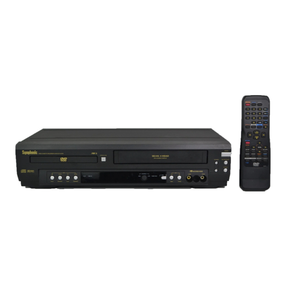
- Page 1 SERVICE MANUAL This service manual supplement (WF803) contains only the difference from the original model. For all other data, see the original service manual for EWD2203. DVD PLAYER & VIDEO CASSETTE RECORDER WF803 POWER OPEN/CLOSE CHANNEL STOP/EJECT PLAY VIDEO AUDIO...
- Page 2 Different parts from original model (EWD2203) Ref. No. Description Part No. FRONT ASSEMBLY H9402UD 0VM204251 TOP COVER(BLACK) H9450UD 0VM306098 DOOR, CASSETTE H9402UD 0VM415465 A10# LABEL, RATING H9402UD ---------- A10# LABEL, RATING H9402UD ---------- LABEL, BAR CODE H9402UD ---------- LABEL, TELEPHONE NUMBER H5720UD ---------- PANEL, TRAY H9402UD 0VM415475...
- Page 3 SERVICE MANUAL Sec. 2: Deck Mechanism Section Sec. 3: Exploded views Sec. 1: Main Section I Standard Maintenance and Parts List Section I Specifications I Alignment for Mechanism I Preparation for Servicing I Exploded views I Disassembly/Assembly of Mechanism I Parts List I Adjustment Procedures I Alignment Procedures of Mechanism I Schematic Diagrams...
- Page 4 IMPORTANT SAFETY NOTICE Proper service and repair is important to the safe, reliable operation of all Funai Equipment. The service procedures recommended by Funai and described in this service manual are effective methods of performing service operations. Some of these service special tools should be used when and as recommended.
-
Page 5: Table Of Contents
MAIN SECTION DVD PLAYER & VIDEO CASSETTE RECORDER DVC860D/EWD2203 Sec. 1: Main Section I Specifications I Preparation for Servicing I Adjustment Procedures I Schematic Diagrams I CBA’s TABLE OF CONTENTS Specifications................1-1-1 Laser Beam Safety Precautions. -
Page 6: Specifications
SPECIFICATIONS < VCR Section > Description Unit Minimum Nominal Maximum Remark 1. Video 1-1. Video Output (PB) Vp-p SP Mode 1-2. Video Output (R/P) Vp-p SP Mode, 1-3. Video S/N Y (R/P) W/O Burst 1-4. Video Color S/N AM (R/P) SP Mode 1-5. - Page 7 < DVD Section > ITEM CONDITIONS UNIT NOMINAL LIMIT 1. Video Output 75 ohm load ± 0.1 2. Coaxial Digital Out 75 ohm load mVpp ± 100 3. Audio (PCM) 3-1. Output Level 1kHz 0dB Vrms 3-2. S/N 3-3. Freq. Response fs=48kHz 20~22kHz ±...
-
Page 8: Laser Beam Safety Precautions
LASER BEAM SAFETY PRECAUTIONS This DVD player uses a pickup that emits a laser beam. Do not look directly at the laser beam coming from the pickup or allow it to strike against your skin. The laser beam is emitted from the location shown in the figure. When checking the laser diode, be sure to keep your eyes at least 30cm away from the pickup lens when the diode is turned on. -
Page 9: Important Safety Precautions
IMPORTANT SAFETY PRECAUTIONS Product Safety Notice I. Also check areas surrounding repaired locations. J. Be careful that foreign objects (screws, solder Some electrical and mechanical parts have special droplets, etc.) do not remain inside the set. safety-related characteristics which are often not evi- K. - Page 10 Safety Check after Servicing Examine the area surrounding the repaired location for damage or deterioration. Observe that screws, parts, Chassis or Secondary Conductor and wires have been returned to their original posi- tions. Afterwards, do the following tests and confirm the specified values to verify compliance with safety Primary Circuit Terminals standards.
-
Page 11: Standard Notes For Servicing
STANDARD NOTES FOR SERVICING Circuit Board Indications How to Remove / Install Flat Pack-IC a. The output pin of the 3 pin Regulator ICs is indi- 1. Removal cated as shown. With Hot-Air Flat Pack-IC Desoldering Machine:. (1) Prepare the hot-air flat pack-IC desoldering Top View Bottom View machine, then apply hot air to the Flat Pack-IC... - Page 12 With Soldering Iron: (4) Bottom of the flat pack-IC is fixed with glue to the CBA; when removing entire flat pack-IC, first apply (1) Using desoldering braid, remove the solder from all soldering iron to center of the flat pack-IC and heat pins of the flat pack-IC.
- Page 13 2. Installation Instructions for Handling Semi-conductors (1) Using desoldering braid, remove the solder from the foil of each pin of the flat pack-IC on the CBA Electrostatic breakdown of the semi-conductors may so you can install a replacement flat pack-IC more occur due to a potential difference caused by electro- easily.
-
Page 14: Preparation For Servicing
PREPARATION FOR SERVICING How to Enter the Service Mode About Optical Sensors Caution: An optical sensor system is used for the Tape Start and End Sensors on this equipment. Carefully read and follow the instructions below. Otherwise the unit may operate erratically. What to do for preparation Insert a tape into the Deck Mechanism Assembly and press the PLAY button. -
Page 15: Operating Controls And Functions
OPERATING CONTROLS AND FUNCTIONS [ DVC860D ] FRONT PANEL POWER OPEN/CLOSE CHANNEL STOP/EJECT PLAY VIDEO AUDIO OUTPUT TIMER REC STOP PLAY F.FWD REMOTE CONTROL 7. POWER Light Lights up when the power is on. 8. STOP/EJECT Button (VCR) POWER SPEED AUDIO EJECT Button Press to remove the tape from the VCR. - Page 16 18. OUTPUT Button 31. TITLE Button 32. SETUP Button Press to select DVD mode or VCR mode. You can switch the output mode either by pressing Press to enter DVD player setup mode. 33. ZOOM Button OUTPUT on the front panel, or by pressing DVD or VCR on the remote control.
- Page 17 48. SLOW Button 44. g Button ● DVD mode During tape playback, press to view the video tape in Press to fast forward the Disc. Press PAUSE, then slow motion. Press again to resume normal playback. This button does not affect DVD playback. press this button to begin slow motion playback.
- Page 18 58. DVD AUDIO OUT Jacks 61. DVD/VCR VIDEO OUT Jack Connect the supplied audio cables here and to the Audio Connect the yellow video cable (supplied) here and to In jacks of a television or other audio equipment (DVD the TV ’...
- Page 19 [ EWD2203 ] FRONT PANEL POWER OPEN/CLOSE CH-UP STOP/EJECT OUTPUT STOP PLAY TIMER VIDEO AUDIO PLAY CH-DOWN PLAY DISC IN REMOTE CONTROL 6. POWER Button Press to turn the power on and off. 7. POWER Light (red) POWER SPEED AUDIO Lights up when the power is on.
- Page 20 18. OUTPUT Button 32. STOP Button ● Press to select DVD mode or VCR mode. DVD mode ● You can switch the output mode either by pressing Press to stop the disc motion. ● OUTPUT on the front panel, or by pressing DVD VCR mode or VCR on the remote control.
- Page 21 ● s Button VCR mode Press to cancel a setting of timer program. Press to While recording, press to temporarily stop the recording (pause). Press a second time to resume correct digits when setting program (For example: setting clock or timer program). Press to add or normal recording.
- Page 22 62. DVD AUDIO OUT Jacks 65. DVD/VCR VIDEO OUT Jack Connect the supplied audio cables here and to the Connect the yellow video cable (supplied) here and Audio In jacks of a television or other audio equip- to the TV ’...
-
Page 23: Cabinet Disassembly Instructions
CABINET DISASSEMBLY INSTRUCTIONS 1. Disassembly Flowchart REMOVAL This flowchart indicates the disassembly steps to gain REMOVE/*UNHOOK/ LOC. PART Fig. access to item(s) to be serviced. When reassembling, UNLOCK/RELEASE/ Note follow the steps in reverse order. Bend, route, and UNPLUG/DESOLDER dress the cables as they were originally. Power 4(S-8) Suppy CBA... - Page 24 Reference Notes CAUTION 1: Locking Tabs (L-1) are fragile. Be careful (S-2) not to break them. (S-2) 1-1. Remove Screw (S-3). [3] Top Bracket 1-2. Release seven Locking Tabs (L-1) (to do this, first release five Locking Tabs (A) at the side and top, and then release two Locking Tabs (B) at the bot- (S-2) tom.)
- Page 25 (S-5) CN201 (S-5) (S-9) [5] DVD Main CBA Unit CN301 [9] Rear Panel (S-8) [8] PCB Bracket [7] Power Supply CBA (S-8) DVD Mecha Fig. D6 Short the three short (S-11) (S-10) lands by soldering (S-10) Slide (S-11) (S-10) (S-11) Pickup Unit [10] VCR Chassis Unit View for A...
- Page 26 Cylinder Assembly FE Head AC Head [11] Deck Assembly Assembly SW507 LD-SW Desolder [12] Main CBA Lead with [11] Deck Assembly blue stripe Cam Gear Hole [12] Main CBA Shaft Hole LD-SW [12] Main CBA [13] DVD OP/CL CBA (S-12) (S-12) Desolder [14] Function CBA...
- Page 27 (S-13) [15] Deck Pedestal (S-13) (S-14) [16] Side Bracket Fig. D9 HOW TO MANUAL EJECT 1. Remove the Top Case. 2. Rotate this roulette in the direction of the arrow as shown below. Top Cover DVD Mecha Tray Deck Assembly Rotate this roulette in the direction of the arrow 1-7-5...
-
Page 28: Electrical Adjustment Instructions
ELECTRICAL ADJUSTMENT INSTRUCTIONS General Note: "CBA" is an abbreviation for "Circuit Board Assembly." NOTE: Figure 1 1.Electrical adjustments are required after replacing circuit components and certain mechanical parts. It is important to do these adjustments only after all EXT. Syncronize Trigger Point repairs and replacements have been completed. -
Page 29: Firmware Renewal Mode
FIRMWARE RENEWAL MODE 1. Turn the power on and remove the disc on the tray. 5. After programming is finished, the tray opens auto- 2. To put the DVD player into version up mode, press matically. Fig. e appears on the screen and the [9], [8], [7], [6], and [SEARCH MODE] buttons on checksum in (*3) of Fig. -
Page 30: Block Diagrams
BLOCK DIAGRAMS <VCR SECTION> Servo/System Control Block Diagram D561 POWER P-ON+9V MAIN CBA IC501 CL509 CL508 (SERVO/SYSTEM CONTROL) POWER-LED AL+5V KEY-1 REMOTE-VIDEO REMOTE-VIDEO KEY- 1 SWITCH FROM/TO DVD SYSTEM SWITCH CONTROL BLOCK DISPLAY-CLK DISPLAY-CLK (DECK ASSEMBLY) TP502 DIAGRAM DISPLAY-DATA DISPLAY-DATA FUNCTION CBA <DVD SECTION>... - Page 31 Video Block Diagram REC VIDEO SIGNAL PB VIDEO SIGNAL DVD VIDEO SIGNAL MODE: SP/REC IC751 (OUTPUT SELECT) TP751 V-OUT Q391 IC501 (OSD) MAIN CBA BUFFER JK751 V-OUT OSD CHARACTER SW CTL FROM 9 10 11 Q760 SERVO/SYSTEM OUTPUT SELECT CONTROL BLOCK DIAGRAM TU701 WF11...
- Page 32 Audio Block Diagram ( DVC860D ) PB-AUDIO SIGNAL REC-AUDIO SIGNAL DVD AUDIO SIGNAL Mode : SP/REC MAIN CBA TU701 FROM DVD VIDEO/ DVD-A(R) AUDIO BLOCK DVD-A(L) DIAGRAM WF10 <DVD SECTION> MOD-A MOD-A IC751 TP753 (OUTPUT SELECT) A-IN (L)-F A-OUT (R) A-IN (R)-F JK751 A-OUT (R)
- Page 33 Audio Block Diagram ( EWD2203 ) PB-AUDIO SIGNAL REC-AUDIO SIGNAL DVD AUDIO SIGNAL Mode : SP/REC MAIN CBA TU701 WF14 AUDIO-OUT DVD-A(R) FROM DVD AUDIO Q763 BLOCK DIAGRAM DVD-A(L) BUFFER <DVD SECTION> WF10 MOD-A Q762 BUFFER IC751 TP753 (OUTPUT SELECT) A-OUT (R) JK751 A-OUT (R)
- Page 34 Hi-Fi Audio Block Diagram ( DVC860D ) PB-AUDIO SIGNAL REC-AUDIO SIGNAL DVD AUDIO SIGNAL Mode : SP/REC MAIN CBA IC451 (MTS/ SAP/ Hi-Fi AUDIO PROCESS/ Hi-Fi HEAD AMP) CONT SERIAL IIC-BUS SDA FROM/TO SERVO/ SYSTEM DATA IIC-BUS SCL CONTROL BLOCK DECODER ST/SAP DEMOD...
- Page 35 CAUTION Power Supply Block Diagram FOR CONTINUED PROTECTION AGAINST FIRE HAZARD, CAUTION ! REPLACE ONLY WITH THE SAME TYPE FUSE. Fixed voltage ( or Auto voltage selectable ) power supply circuit is used in this unit. NOTE : ATTENTION : POUR UNE PROTECTION CONTINUE LES RISQES If Main Fuse (F001) is blown, check to see that all components in the power supply The voltage for parts in hot circuit is measured using D'INCELE N'UTILISER QUE DES FUSIBLE DE MEMO TYPE.
- Page 36 BLOCK DIAGRAMS<DVD SECTION> DVD System Control/Servo Block Diagram SLED SERVO SIGNAL SPINDLE SERVO SIGNAL FOCUS SERVO SIGNAL TRACKING SERVO SIGNAL IC101 SW2001 (MICRO CONTROLLER) CL2003 CL2002 OPEN OPEN/CLOSE 2 EXT CLOCK /CLOSE EWD2203 CLK33M AL+5V OPEN/CLOSE CBA BE CLOCK IC451 D2001 D2002 (CLOCK GENERATOR)
- Page 37 Digital Signal Process Block Diagram DATA(AUDIO) SIGNAL DATA(VIDEO/AUDIO) SIGNAL DVD VIDEO SIGNAL IC102 (SDRAM) IC101 (MICRO CONTROLLER) SDRAM ADDRESS(0-10) SDRAM ADDRESS(0-10) DATA SDRAM EXTERNAL MEMORY DECODER INST. DECODER STREAM SDRAM DATA(0-31) SDRAM DATA(0-31) DATA PIXEL OPERATION INST. DATA CN201 DVD/CD SIGNAL PROCESSOR INST.
- Page 38 DVD Video / Audio Block Diagram DVD VIDEO SIGNAL DATA(AUDIO) SIGNAL DVD AUDIO SIGNAL IC1402 (VIDEO DRIVER) DRIVER JK1401 S-VIDEO OUT DRIVER CN601 CN1601 DRIVER VIDEO-Y VIDEO-Y FROM DIGITAL VIDEO-C VIDEO-C SIGNAL PROCESS VIDEO-Cb DRIVER VIDEO-Cb DVD-VIDEO TO VIDEO BLOCK DIAGRAM VIDEO-Cr BLOCK DIAGRAM VIDEO-Cr...
-
Page 39: Schematic Diagrams / Cba's And Test Points
SCHEMATIC DIAGRAMS / CBA’S AND TEST POINTS Standard Notes WARNING Many electrical and mechanical parts in this chassis have special characteristics. These characteristics often pass unnoticed and the protection afforded by them cannot necessarily be obtained by using replace- ment components rated for higher voltage, wattage, etc. - Page 40 LIST OF CAUTION, NOTES, AND SYMBOLS USED IN THE SCHEMATIC DIAGRAMS ON THE FOLLOWING PAGES: 1. CAUTION: FOR CONTINUED PROTECTION AGAINST FIRE HAZARD, REPLACE ONLY WITH THE SAME TYPE FUSE. ATTENTION: POUR UNE PROTECTION CONTINUE LES RISQES D'INCELE N'UTILISER QUE DES FUSIBLE DE MEMO TYPE.
- Page 41 Main 1/8 Schematic Diagram < VCR Section > MAIN 1/8 Schematic Diagram REC Video Signal PB Video Signal Parts Location Guide REC Audio Signal PB Audio Signal Ref No. Position IC501 COILS L501 L502 L503 TRANSISTORS Q501 Q506 VARIABLE RESISTORS VR501 TEST POINTS TP505...
- Page 42 Main 2/8 Schematic Diagram < VCR Section > MAIN 2/8 Schematic Diagram REC Video Signal DVD Video + PB Video Signal Note: Parts Location Guide PB Audio Signal When it is necessary to replace one or more of the following Diodes, REC Audio Signal Ref No.
- Page 43 Main 3/8 Schematic Diagram < VCR Section > MAIN 3/8 Schematic Diagram REC Video Signal PB Video Signal Parts Location Guide DVD Video + PB Video Signal REC Audio Signal Ref No. Position PB Audio Signal IC301 COILS L251 L303 L304 L421 L422...
- Page 44 Main 4/8 Schematic Diagram ( DVC860D ) < VCR Section > MAIN 4/8 Schematic Diagram REC Audio Signal PB Audio Signal Parts Location Guide SPINDLE SERVO SIGNAL Ref No. Position IC451 COILS L451 TEST POINTS TP452 1-11-9 1-11-10 H9400SCM4...
- Page 45 Main 5/8 Schematic Diagram < VCR Section > MAIN 5/8 Schematic Diagram Parts Location Guide VIDEO SIGNAL SPINDLE SERVO SIGNAL DATA(AUDIO) Ref No. Position IC1201 IC1402 COILS L1350 L1351 BB-1 L1401 AA-1 L1441 AA-1 L1442 AA-1 L1461 AA-1 L1481 AA-1 L1521 TRANSISTORS Q1201...
- Page 46 Main 6/8 Schematic Diagram < VCR Section > VIDEO Signal MAIN 6/8 Schematic Diagram REC Video Signal Parts Location Guide PB Video Signal REC Audio Signal DVD Video + PB Video Signal Ref No. Position PB Audio Signal SPINDLE SERVO Signal IC751 DD-3 TRANSISTORS...
- Page 47 Main 7/8 Schematic Diagram < VCR Section > Note: MAIN 7/8 Schematic Diagram When it is necessary to replace one or more of the following Diodes, Parts Location Guide all two should be replaced: D2001, D2002. Ref No. Position COILS L2001 KK-1 TRANSISTORS...
- Page 48 Main 8/8 Schematic Diagram < VCR Section > MAIN 8/8 Schematic Diagram Parts Location Guide Ref No. Position IC1002 NN-3 IC1004 OO-1 COILS L1009 OO-1 L1010 OO-2 TRANSISTORS Q052 QQ-4 Q055 PP-3 Q056 QQ-3 Q057 PP-3 Q1004 PP-1 Q1005 NN-2 Q1006 OO-2 Q1011...
- Page 49 Power Supply Schematic Diagram < VCR Section > Power Supply Schematic Diagram CAUTION CAUTION ! NOTE : Parts Location Guide FOR CONTINUED PROTECTION AGAINST FIRE HAZARD, Fixed voltage ( or Auto voltage selectable ) power supply circuit is used in this unit. The voltage for parts in hot circuit is measured using Ref No.
- Page 50 Function Schematic Diagram < VCR Section > DVD SW CBA Top View DVD SW CBA Bottom View Note: When it is necessary to replace one or more of the following Diodes, all one should be replaced: D561. BH9400F01011D DVD OP/CL CBA Top View DVD OP/CL CBA Bottom View BH9400F01011C H9400SCF...
- Page 51 Main CBA Top View Sensor CBA Top View BHB300F01014-A TP751 BHB300F01014-B V-OUT TP513 TP302 RF-SW TP301 VR501 C-PB SW-P TP502 S-INH 1-11-23 1-11-24 BH9400F01011A...
- Page 52 Main CBA Bottom View MAIN CBA Parts Location Guide Ref No. Position Ref No. Position Ref No. Position Ref No. Position Ref No. Position Ref No. Position Ref No. Position COILS COILS TRANSISTORS TRANSISTORS TRANSISTORS TEST POINTS IC301 L421 L1442 Q391 Q567 Q1385...
- Page 53 Power Supply CBA Top View Power Supply CBA Bottom View CAUTION CAUTION ! BECAUSE A HOT CHASSIS GROUND IS PRESENT IN THE POWER Fixed voltage ( or Auto voltage selectable ) power supply circuit is used in this unit. FOR CONTINUED PROTECTION AGAINST FIRE HAZARD, SUPPLY CIRCUIT , AN ISOLATION TRANSFORMER MUST BE USED.
- Page 54 DVD Main 1/3 Schematic Diagram < DVD Section > TRACKING SERVO SIGNAL SLIDE SERVO SIGNAL DVD MAIN 1/3 Schematic Diagram DATA(VIDEO+AUDIO) Parts Location Guide Ref No. Position FOCUS SERVO SIGNAL SPINDLE SERVO SIGNAL IC201 IC202 IC301 IC461 TRANSISTORS Q251 Q252 Q253 Q254 1-11-29...
- Page 55 DVD Main 2/3 Schematic Diagram < DVD Section > DATA(VIDEO+AUDIO) TRACKING SERVO SIGNAL SLIDE SERVO SIGNAL DVD MAIN 2/3 Schematic Diagram FOCUS SERVO SIGNAL SPINDLE SERVO SIGNAL Parts Location Guide Ref No. Position IC101 1-11-31 1-11-32 H9400SCD2...
- Page 56 IC101 VOLTAGE CHART PIN.NO PLAY STOP PIN.NO PLAY STOP PIN.NO PLAY STOP PIN.NO PLAY STOP PIN.NO PLAY STOP PIN.NO PLAY STOP PIN.NO PLAY STOP PIN.NO PLAY STOP ----- ----- ----- ----- ----- ----- ----- ----- ----- ----- ----- ----- ----- ----- ----- -----...
- Page 57 DVD Main 3/3 Schematic Diagram < DVD Section > DVD MAIN 3/3 Schematic Diagram Parts Location Guide DATA(AUDIO) VIDEO SIGNAL SPINDLE SERVO SIGNAL Ref No. Position IC102 IC103 IC104 IC105 IC451 IC601 H9400SCD3 1-11-35 1-11-36...
-
Page 58: Waveforms
WAVEFORMS (TP751 of Main CBA) Pin 5 of CN1601 WF 1 V-OUT E-E VIDEO-Y 0.2V 20µsec 10usec 50mV x 10 (TP751 of Main CBA) UPPER Pin 7 of CN1601 (TP302 of Main CBA) LOWER V-OUT 0.1V x 10 RF-SW 0.5V x 10 VIDEO-C 0.2V 20µsec... - Page 59 WAVEFORMS (Pin 12 of TU701) WF13 Pin 11 of CN1601 WF10 (Pin 2 of TU701) AUDIO-L 0.5msec MOD-A 20mV x 10 0.2msec PLL-DATA 0.1V x 10 2msec WF14 (Pin 14 of TU701) Pin 13 of CN1601 (Pin 6 of TU701) WF11 AUDIO-R TU AUDIO...
- Page 60 WIRING DIAGRAM < VCR SECTION > FRONT REAR (DECK ASSEMBLY) VIDEO AUDIO AUDIO S-VIDEO AUDIO AUDIO VIDEO AUDIO AUDIO VIDEO AUDIO AUDIO DIGITAL VIDEO-Cr VIDEO-Y VIDEO-Cb IN (R) IN (L) OUT (R) OUT (L) IN (R) IN (L) OUT (R) OUT (L) AUDIO OUT MAIN CBA...
- Page 61 WIRING DIAGRAM < DVD SECTION > DVD MECHA CN401 EV+1.5V EV+1.5V SENSOR EV+1.5V EV+3.3V TRAY-OUT EV+3.3V FG CBA CN301 FG-IN DVD-P-ON+3.3V TRAY-IN SP(+) SP(-) TRAY-OUT SPINDLE TO MAIN CBA TRAY-IN MOTOR CN1001 DVD-P-ON+5V SLED 8 SL(-) EV+9V MOTOR 9 SL(+) EV+9V FP-STB DVD-P-ON+3.3V...
-
Page 62: System Control Timing Charts
SYSTEM CONTROL TIMING CHARTS [ VCR Section ] Mode SW : LD-SW LD-SW Position detection A/D Input voltage Limit Symbol (Calculated voltage) 3.76V~4.50V (4.12V) 4.51V~5.00V (5.00V) 0.00V~0.25V (0.00V) 1.06V~1.50V (1.21V) 0.66V~1.05V (0.91V) 1.99V~2.60V (2.17V) 1.51V~1.98V (1.80V) 3.20V~3.75V (3.40V) 0.26V~0.65V (0.44V) 4.51V~5.00V (5.00V) 2.61V~3.19V... - Page 63 Still/Slow Control Frame Advance Timing Chart 1) SP Mode 18 RF-SW The first rise of RF-SW after a rise in F-AD signal F-AD (Internal Signal) "H" "H" "Z" C-DRIVE "L" "L" Stop detection (T2) Acceleration Detection (T1) Slow Tracking Value PB CTL Reversal Limit Value 20ms...
- Page 64 2) LP/SLP Mode 18 RF-SW The first rise of RF-SW after a rise in F-AD signal F-AD (Internal Signal) "H" "H" "Z" C-DRIVE "L" "L" Stop detection (T2) Acceleration Detection (T1) Slow Tracking Value PB CTL Reversal Limit Value 20ms 27 C-F/R 79 H-A-SW 78 ROTA...
- Page 65 EJECT ST-S/ END-S "OFF" CASS.LOAD LD-FWD 0.2S LD-REV 0.7S LD-FWD 0.4S LD-FWD 0.2S LD-REV 0.2S LD-FWD 0.5S LD-REV STOP(A) PLAY LD-FWD PLAY LD-FWD LD-REV 0.2S LD-FWD PLAY PLAY PAUSE (SLOW) LD-FWD STILL(SLOW) PLAY LD-REV 0.2S LD-FWD PLAY STOP /EJECT LD-REV STOP(A) Fig.
- Page 66 STOP(A) STOP LD-REV 0.2S LD-FWD STOP /EJECT 1.0S LD-FWD 0.5S LD-REV STOP(A) LD-REV 0.2S LD-FWD STOP /EJECT LD-REV 1.0S LD-FWD 0.5S LD-REV STOP(A) LD-FWD PAUSE LD-FWD 2.5S Short REV LD-REV 0.2S LD-FWD REC PAUSE REC or PAUSE STOP /EJECT LD-FWD 1.5S LD-REV 0.2S...
- Page 67 [ DVD Section ] Tray Close ~ Play / Play ~ Tray Open Disc Tray Tray Disc Stop Open Close Rotation Play 3.3V Tray OUT (TL220) 3.3V Tray IN (TL221) 1.65V Sled Drive (TP303) 1.65V Disc Drive (TP301) 1.65V Focus Drive (TP304) 1.65V Tracking Drive...
-
Page 68: Ic Pin Function Descriptions
IC PIN FUNCTION DESCRIPTIONS [ VCR Section ] Signal Active Mark Function Name Level Comparison Chart of Models and Marks Top Speed Select Signal Model Mark SP/LP/ (SP=”L”/ H/Z/L LP=”Z”/ DVC860D SLP=”H”) EWD2203 N.U. Not Used Input Selector IC501( SERVO / SYSTEM CONTROL IC ) Control Signal INSEL/ H/Hi-z... - Page 69 Signal Active Signal Active Mark Function Mark Function Name Level Name Level Main Clock CTL Amp. AC CTLA OUT OSCO Output 14.31818MHz AVDD AVDD Main Clock Playback/ OSCI Input Record Control CTL (+) 14.31818MHz Signal (+) Playback/ Record Control CTL (-) Sub Clock Signal (-) Input 32.768...
- Page 70 [ DVD Section ] Signal Active Mark Function Name Level DVC860D DVD Mode LED Signal OUT REC-IND Output IC571 [ PT6313-S-TP ] REC Mode Signal VCR/TV- LED Signal In/Out Name Function Name Output Clock Input N.U. Not Used N.U. Not Used Serial Interface Strobe TIMER- “TIMER”...
-
Page 71: Lead Identifications
LEAD IDENTIFICATIONS BN1L3Z(P) KTC3202(Y) NJM4558D 2SK2662 BA1L3Z-T 2SC1815-BL(TPE2) KIA4558P KIA78R33PI BN1F4M-T 2SC1815-Y(TPE2) PQ3RD13(1A) BA1F4M-T 2SC1815-GR(TPE2) KTA1266(GR) 2SC3331(T,U) KTC3193(Y) 2SC2120-Y(TPE2) KTC3199(Y,GR,BL) KTC3203(Y) 2SC2785(J,H,F,K) KTC3205 (Y) KRC103M 2SA1015-GR(TPE2) KRA103M KTC3198(Y,GR) KTA1273(Y) 2SA966(Y) KRA110M 2SC2236-Y-TPE6, C KRC110M-AT E C B E C B G D S 2SC536NF(NG)-NPA-AT PT6313-S-TP... - Page 72 DECK MECHANISM SECTION DVD PLAYER & VIDEO CASSETTE RECORDER DVC860D/EWD2203 Sec. 2: Deck Mechanism Section I Standard Maintenance I Alignment for Mechanism I Disassembly/Assembly of Mechanism I Alignment Procedures of Mechanism TABLE OF CONTENTS Standard Maintenance..............2-1-1 Service Fixtures and Tools.
-
Page 73: Standard Maintenance
STANDARD MAINTENANCE Service Schedule of Components H: Hours : Check I: Change Deck Periodic Service Schedule Ref.No. Part Name 1,000 H 2,000 H 3,000 H 4,000 H Cylinder Assembly Loading Motor Assembly Pulley Assembly B587 Tension Lever Assembly AC Head Assembly B573,B574 Reel (SP)(D2), Reel (TU)(D2) Capstan Motor... - Page 74 Cleaning Cleaning of Audio Control Head Clean the head with a cotton swab. Cleaning of Video Head Procedure Clean the head with a head cleaning stick or chamois 1.Remove the top cabinet. cloth. 2.Dip the cotton swab in 90% isopropyl alcohol and Procedure clean the audio control head.
-
Page 75: Service Fixtures And Tools
SERVICE FIXTURE AND TOOLS J-1-1, J-1-2 Ref. No. Name Part No. Adjustment J-1-1 Alignment Tape FL8A Head Adjustment of Audio Control Head J-1-2 Alignment Tape FL8N Azimuth and X Value Adjustment of Audio Control (2Head only) Head / Adjustment of Envelope Waveform FL8NW (4Head only) Guide Roller Adj.Screwdriver... -
Page 76: Mechanical Alignment Procedures
MECHANICAL ALIGNMENT PROCEDURES Explanation of alignment for the tape to correctly run B. Method to place the Cassette Holder in the tape- starts on the next page. Refer to the information below loaded position without a cassette tape on this page if a tape gets stuck, for example, in the 1. - Page 77 1.Tape Interchangeability Alignment Note: To do these alignment procedures, make sure that the Tracking Control Circuit is set to the center position every time a tape is loaded or unloaded. (Refer to page 2-3-4, procedure 1-C, step 2.) Equipment required: Dual Trace Oscilloscope VHS Alignment Tape (FL8NW) Guide Roller Adj.
- Page 78 1-A. Preliminary/Final Checking and 3. Check to see that the tape runs without creasing at Alignment of Tape Path Take-up Guide Post [4] or without snaking between Guide Roller [3] and AC Head. (Fig. M3 and M5) Purpose: 4. If creasing or snaking is apparent, adjust the Tilt To make sure that the tape path is well stabilized.
- Page 79 6. Press CH DOWN button on the unit until the CTL 1-D. Azimuth Alignment of Audio/Control/ Erase Head waveform has shifted from its original position (not the position achieved in step 5, but the position of Purpose: CTL waveform in step 4) by approximately -2msec. To correct the Azimuth alignment so that the Audio/ Make sure that the envelope is simply attenuated Control/Erase Head meets tape tracks properly.
-
Page 80: Disassembly/Assembly Procedures Of Deck Mechanism
DISASSEMBLY/ASSEMBLY PROCEDURES OF DECK MECHANISM Before following the procedures described below, be sure to remove the deck assembly from the cabinet. (Refer to CABINET DISASSEMBLY INSTRUCTIONS on page 1-7-1.) All the following procedures, including those for adjustment and replacement of parts, should be done in Eject mode;... - Page 81 REMOVAL INSTALLATION STEP START- REMOVE/*UNHOOK/ /LOC. PART ADJUSTMENT Fig. No. UNLOCK/RELEASE/ CONDITION UNPLUG/DESOLDER Loading Arm (TU) (+)Refer to Alignment [32] [33] DM2,DM14 Assembly Sec.Pg.2-4-9 [34] [2],[25] M Brake (TU) Assembly DM1,DM15 *(P-7), Brake Belt [35] [2],[25] M Brake (SP) Assembly DM1,DM15 *(P-8) [36] [35]...
- Page 82 Top View [41] [42] [46] [43] [14] [13] [11] [15] [36] [10] [12] [35] [34] [40] [29] [30] [16] [39] [38] Fig. DM1 Bottom View [20] [33] [32] [24] [26] [27] [25] [23] [28] [22] [21] [31] Fig. DM2 2-4-3 H9400DA...
- Page 83 (S-1) (S-1) (L-1) (L-3) (L-2) (P-1) Fig. DM5 [46] Fig. DM3 [47] Pin D (L-14) Pin C Pull up Slide Pin A Pin B Slot A (S-2) Slots B Slot A First, while pushing the locking tab as shown at right, slide and pull up the right side on [2] to release Pin A and Pin B from the slots A.
- Page 84 (S-4) (S-5) [14] (S-6) [16] [15] Desolder from bottom (S-3) Lead with White Stripe Belt View for A Fig. DM7 Fig. DM9 Adj. Screw [11] [18] (L-4) (L-5) (P-3) [17] [13] [19] [12] (P-4) [10] (P-2) (S-7) Pin of [12] Pin of [10] Fig.
- Page 85 [22] (C-4) (S-8) (C-1) [23] (L-6) [21] (P-5) [20] Cap Belt (P-5) [28] Fig. DM11 When installing [23], install the spring (P-5) to [28] as shown in the left figure, and then install [23] while Pin on pressing the spring (P-5) to bottom the direction of the arrow in of [23]...
- Page 86 (P-6) [25] [31] Refer to the Alignment (C-3) Section, Page 2-4-9. (S-9) [29] [33] [30] (L-11) [32] (L-10) (L-8) (C-2) [27] [28] [24] [26] (L-9) Fig. DM14 [36] Position of Mode Lever when installed Break belt Pin of [35] (P-7) Pin of [31] Pin of [34] [34]...
- Page 87 [42] [41] [43] (L-13) Fig. DM16 [44] [45] Slide Fig. DM17 2-4-8 H9400DA...
-
Page 88: Alignment Procedures Of Mechanism
ALIGNMENT PROCEDURES OF MECHANISM The following procedures describe how to align the Alignment 1 individual gears and levers that make up the tape Loading Arm (SP) and (TU) Assembly loading/unloading mechanism. Since information about the state of the mechanism is provided to the Install Loading Arm (SP) and (TU) Assembly so System Control Circuit only through the Mode Switch, that their triangle marks point to each other as... - Page 89 EXPLODED VIEWS AND PARTS LIST SECTION DVD PLAYER & VIDEO CASSETTE RECORDER DVC860D/EWD2203 Sec. 3: Exploded views and Parts List Section I Exploded views I Parts List TABLE OF CONTENTS Exploded Views ............... . 3-1-1 Mechanical Parts List.
-
Page 90: Exploded Views
EXPLODED VIEWS Cabinet 2L041 2L041 See Electrical Parts List for parts with this mark. 2L041 2L071 Some Ref. Numbers are 2L071 W014 2L071 not in sequence. 2L041 2L071 L1-A 2L041 L1-B W017 2L071 2B33 DVD Main 2B18 CBA Unit W011 2L033 2L021 2L013... - Page 91 Packing X46 [EWD2203] Unit 2B36 [EWD2203] 3-1-3 H9400PEX...
- Page 92 DECK EXPLODED VIEWS Deck Mechanism View 1 Mark Description Floil G-684G or Multemp MH-D (Blue grease) SLIDUS OIL #150 B494 L1467 L1191 B553 B411 B567 L1053 B410 L1051 Chassis Assembly Top View (Lubricating Point) B501 B560 L1450 L1450 B426 L1466 B121 B126 B492...
- Page 93 Deck Mechanism View 2 Mark Description Floil G-684G or Multemp MH-D (Blue grease) B587 B521 B487 SLIDUS OIL #150 B416 B591 SANKOUL FG84M (Yellow grease) B520 B590 B522 B499 L1406 B148 B508 B573 B592 B574 B558 B564 B557 B414 B565 B525 L1151 B417...
- Page 94 Deck Mechanism View 3 Mark Description Floil G-684G or Multemp MH-D (Blue grease) SLIDUS OIL #150 L1321 B347 L1321 B355 B354 B483 B425 B482 B562 B300 B563 B313 B529 B360 B359 B361 B555 B303 Some Ref. Numbers are not in sequence. B514 3-1-6 H9400DEX...
-
Page 95: Mechanical Parts List
MECHANICAL PARTS LIST PRODUCT SAFETY NOTE: Products marked with a Ref. No. Mark Description Part No. # have special characteristics important to safety. 2L052 SCREW, P-TIGHT M3X6 BIND HEAD+ GBMP3060 Before replacing any of these components, read care- 2L054 SCREW, P-TIGHT M3X6 BIND HEAD+ GBMP3060 fully the product safety notice in this service manual. -
Page 96: Electrical Parts List
ELECTRICAL PARTS LIST PRODUCT SAFETY NOTE: Products marked with a Ref. No. Mark Description Part No. # have special characteristics important to safety. ELECTROLYTIC CAP. 100µF/25V M CE1EMASTL101 Before replacing any of these components, read care- C051 ELECTROLYTIC CAP. 10µF/16V M H7 CE1CMAVSL100 fully the product safety notice in this service manual. - Page 97 Ref. No. Mark Description Part No. Ref. No. Mark Description Part No. CHIP CERAMIC CAP . B K 0.047µF/25V or CHD1EKB0B473 C410 CHIP CERAMIC CAP . F Z 0.1µF/25V or CHD1EZ30F104 CHIP CERAMIC CAP . B K 0.047µF/50V or CHD1JK30B473 CHIP CERAMIC CAP .
- Page 98 Ref. No. Mark Description Part No. Ref. No. Mark Description Part No. C471 ELECTROLYTIC CAP . 22µF/6.3V M H7 CE0KMAVSL220 C515 CHIP CERAMIC CAP . CG J 18pF/50V or CHD1JJ3CG180 C472 CHIP CERAMIC CAP .(MELF) Y K 4700pF/ CZM1CK30Y472 CHIP CERAMIC CAP . CH J 18pF/50V or CHD1JJ3CH180 16V or CHIP CERAMIC CAP .
- Page 99 Ref. No. Mark Description Part No. Ref. No. Mark Description Part No. FILM CAP .(P) 0.039µF/50V J CMA1JJS00393 CHIP CERAMIC CAP . B K 1000pF/50V CHD1JKB0B102 C708 ELECTROLYTIC CAP . 0.22µF/50V M or CE1JMASDLR22 C1245 CHIP CERAMIC CAP . F Z 0.1µF/25V or CHD1EZ30F104 ELECTROLYTIC CAP .
- Page 100 Ref. No. Mark Description Part No. Ref. No. Mark Description Part No. C2012 CHIP CERAMIC CAP . F Z 0.1µF/25V or CHD1EZ30F104 D2001 LED(GREEN) LTL-4231N NPQZLTL4231N CHIP CERAMIC CAP . F Z 0.1µF/25V or CHD1EZB0F104 D2002 LED(GREEN) LTL-4231N NPQZLTL4231N CHIP CERAMIC CAP . F Z 0.1µF/50V or CHD1JZ30F104 CHIP CERAMIC CAP .
- Page 101 Ref. No. Mark Description Part No. Ref. No. Mark Description Part No. Q421 TRANSISTOR 2SA1015-GR(TPE2) or QQS102SA1015 TRANSISTOR 2SC2785(H) or QQSH02SC2785 TRANSISTOR KTA1266(GR) NQS40KTA1266 TRANSISTOR 2SC2785(J) or QQSJ02SC2785 Q422 TRANSISTOR 2SC2120-Y(TPE2) or QQSY02SC2120 TRANSISTOR KTC3199(GR) or NQS10KTC3199 TRANSISTOR KTC3203(Y) NQSY0KTC3203 TRANSISTOR KTC3199(Y) NQSY0KTC3199 Q423...
- Page 102 Ref. No. Mark Description Part No. Ref. No. Mark Description Part No. CHIP RES.(1608) 1/10W J 1.8k Ω TRANSISTOR KTC3199(Y) NQSY0KTC3199 RRXAJR5Z0182 CHIP RES.(1608) 1/10W J 1.8k Ω or Q2003 TRANSISTOR 2SC1815-GR(TPE2) or QQS102SC1815 R330 RRXAJB5Z0182 CHIP RES.(1608) 1/10W J 1.8k Ω TRANSISTOR 2SC1815-Y(TPE2) or QQSY02SC1815 RRXAJR5Z0182...
- Page 103 Ref. No. Mark Description Part No. Ref. No. Mark Description Part No. CARBON RES. 1/4W J 820 Ω or CHIP RES.(1608) 1/10W J 15k Ω R426 RCX4JATZ0821 RRXAJR5Z0153 CARBON RES. 1/6W J 820 Ω CHIP RES.(1608) 1/10W J 47k Ω or RCX6JATZ0821 R486 RRXAJB5Z0473...
- Page 104 Ref. No. Mark Description Part No. Ref. No. Mark Description Part No. CHIP RES.(1608) 1/10W J 10k Ω CHIP RES.(1608) 1/10W J 3.9k Ω RRXAJR5Z0103 RRXAJR5Z0392 CHIP RES.(1608) 1/10W J 10k Ω or CHIP RES.(1608) 1/10W J 330 Ω or R546 RRXAJB5Z0103 R701...
- Page 105 Ref. No. Mark Description Part No. Ref. No. Mark Description Part No. CHIP RES.(1608) 1/10W J 3.9k Ω CHIP RES.(1608) 1/10W J 100k Ω or RRXAJR5Z0392 R1240 RRXAJB5Z0104 CHIP RES.(1608) 1/10W J 10k Ω or CHIP RES.(1608) 1/10W J 100k Ω R1086 RRXAJB5Z0103 RRXAJR5Z0104...
- Page 106 Ref. No. Mark Description Part No. Ref. No. Mark Description Part No. CHIP RES.(1608) 1/10W J 10k Ω or R2006 RRXAJB5Z0103 FIP502 V.F.D. 7-BT-292GN or TVFD150FT010 CHIP RES.(1608) 1/10W J 10k Ω RRXAJR5Z0103 V.F.D. 20U29100SAN TVFD150FT007 CHIP RES.(1608) 1/10W 0 Ω or CHIP RES.(1608) 1/10W 0 Ω...
- Page 107 Ref. No. Mark Description Part No. Ref. No. Mark Description Part No. CHIP RES.(1608) 1/10W J 1.2k Ω RRXAJR5Z0122 TRANSISTORS CHIP RES.(1608) 1/10W J 1.5k Ω or R587 RRXAJB5Z0152 Q503 PHOTO TRANSISTOR PT204-6B-12 or NPWZT2046B12 CHIP RES.(1608) 1/10W J 1.5k Ω RRXAJR5Z0152 PHOTO TRANSISTOR MID-32A22 NPWZM1D32A22...
- Page 108 Ref. No. Mark Description Part No. Ref. No. Mark Description Part No. METAL OXIDE FILM RES. 1W J 0.68 Ω RECTIFIER DIODE BA157 NDQZ000BA157 RN01R68ZU001 CHIP RES.(1608) 1/10W F 2.2k Ω or D1001 RECTIFIER DIODE 1N4005 NDQZ001N4005 R1019 RRXAFR5H2201 CHIP RES.(1608) 1/10W F 2.2k Ω D1002 RECTIFIER DIODE 1N4005 NDQZ001N4005...
-
Page 109: Deck Parts List
DECK PARTS LIST Comparison Chart of Models and Marks Ref.No Mark Description Part No. B499 T LEVER HOLDER MK12 0VM305729 Model Mark B501 WORM HOLDER MK12 0VM203767 DVC860D B502 CAM GEAR(B) MK12 0VM305721 EWD2203 B507 REEL WASHER MK9 5*2.1*0.5 0VM410058 B508 S BRAKE SPRING MK10 0VM411121... - Page 110 Printed in Japan 2003-03-14 HO...